We demonstrate the use of the Laser-induced forward transfer technique (LIFT) for the printing of high-viscosity Ag paste. This technique offers a simple, low temperature, robust process for non-lithographically printing microscale 2D and 3D structures.
Method Article
Laser-induced Forward Transfer of Ag Nanopaste
In This Article
Summary
Abstract
Over the past decade, there has been much development of non-lithographic methods1-3 for printing metallic inks or other functional materials. Many of these processes such as inkjet3 and laser-induced forward transfer (LIFT)4 have become increasingly popular as interest in printable electronics and maskless patterning has grown. These additive manufacturing processes are inexpensive, environmentally friendly, and well suited for rapid prototyping, when compared to more traditional semiconductor processing techniques. While most direct-write processes are confined to two-dimensional structures and cannot handle materials with high viscosity (particularly inkjet), LIFT can transcend both constraints if performed properly. Congruent transfer of three dimensional pixels (called voxels), also referred to as laser decal transfer (LDT)5-9, has recently been demonstrated with the LIFT technique using highly viscous Ag nanopastes to fabricate freestanding interconnects, complex voxel shapes, and high-aspect-ratio structures. In this paper, we demonstrate a simple yet versatile process for fabricating a variety of micro- and macroscale Ag structures. Structures include simple shapes for patterning electrical contacts, bridging and cantilever structures, high-aspect-ratio structures, and single-shot, large area transfers using a commercial digital micromirror device (DMD) chip.
Introduction
Additive printing techniques are of considerable interest for the patterning of functional materials onto a variety of substrates. These so-called "direct-write" processes, including micropen10, direct-write assembly11, inkjet12, and LIFT4, are well suited for the fabrication of a variety of feature sizes ranging from sub-micron to macroscale1,2. The primary advantages of these techniques are low cost, environmental friendliness, and fast turnaround from concept to prototype. Indeed, rapid prototyping is a primary use for such processes. The materials utilized by these processes typically consist of a nanoparticle suspension within a solvent, and generally require a furnace curing step after deposition in order to realize their functional properties. Although micropen and direct-write assembly are relatively simple to implement, both rely on a continuous filament contact with the receiving substrate during dispensing. Although inkjet is a simple, non-contact direct-write method, it is usually limited to the transfer of low viscosity, chemically benign nanoparticle suspensions in order to avoid clogging and/or corrosion of the dispensing nozzles. In addition, printing patterns with well-defined edge features by inkjet is very difficult given the variable behavior of fluids on different surfaces and their resulting instability due to wetting effects13. Regardless, inkjet has enjoyed the most attention from researchers thus far.
LIFT, on the other hand, is a non-contact, nozzle-free additive process which is capable of transferring high-viscosity paste with well-defined edges. In this process, controlled amounts of complex materials are transferred from a donor substrate (or "ribbon") to a receiving substrate by using laser pulses4 as shown schematically in Figure 1. When using high viscosity paste, it is possible for the printed voxel to match the size and shape of the incident laser pulse cross section5. This process has been referred to as laser decal transfer (LDT), and offers a unique approach to direct-writing in which voxel shape and size are readily controllable parameters, allowing the non-lithographic generation of structures for a wide range of applications such as circuit repair14, metamaterials7, interconnects8, and free-standing structures15. The ability to deposit complex shapes in one transfer step greatly reduces the processing time and avoids problems related to the merging of multiple voxels, a common problem in most digital printing techniques. The ability to dynamically adjust the spatial profile of individual laser pulses17 serves to increase the writing speed of LDT as compared to other laser direct write (LDW) techniques. As a result of these processing advantages, we refer to the LDT process as being "partially parallelized" since it allows the combination of multiple serial writing steps into a single parallel one. The degree of parallelization ultimately depends on the ability to rapidly alter the laser cross-section profile, and therefore the shape of the resultant voxel, and on the speed by which the ribbon and substrate can be translated.
To help visualize the process, the behavior of a material during the LIFT process is depicted schematically in Figures 2A, 2C, and 2E for three different paste viscosities. For low viscosity inks (Figure 2A)9, the transfer process follows jetting behavior, resulting in the formation of rounded, hemispherical voxels (Figure 2B)18. Figure 2C depicts the transfer for very high viscosity suspensions, in which the ejected voxel experiences fragmentation similar to what is observed with LIFT of solid ceramic layers19. Figure 2E depicts the LDT transfer of nanopaste with a suitable, intermediate viscosity, wherein the released voxel is not subject to shape deformation due to surface tension effects and reaches the receiving substrate intact. The effect of viscosity on the shape of the transferred voxels is shown in the atomic force microscopy (AFM) images in Figures 2B, 2D, and 2F. As Figure 2F demonstrates, it is possible to obtain sharp, well-defined voxels for an appropriate range of viscosities, usually ~100 Pa·sec for Ag nanopaste5.
Overall, there have been few reports of methods that combine non-contact printing with the potential for micron resolution 3D structures. The LDT method offers a freeform process capable of fabricating interconnects with ultra-fine pitch bonding capabilities. A number of applications including delicate electronic devices, organic electronics, and microelectromechanical systems (MEMS) could benefit from such a process. Here we demonstrate a process for non-contact, three-dimensional printing as well as single-laser-shot, large area printing (via DMD chip) of high-viscosity Ag nanopaste.
Protocol
1. Making Donor Substrates
- Mask the edges of a glass slide with tape leaving a central region of uncovered glass.
- Submerge the slide in Buffered HF (6:1 ratio of 40% NH4F in water to 48% HF in water) for 3-15 min. Note: This will etch the center of the slide which is unmasked, creating a well. The depth of the well should be between 1 and 5 µm, which can be determined through a stylus profilometer or AFM using manufacturer's instructions.
- Remove the tape mask.
2. Creating the Ink Ribbon
- Spread a small amount of Ag paste at one side of the well. Ensure that there is enough to fill the well, roughly in the 10 mg range. It is not necessary to measure the amount first, however.
- Firmly drag a straight metal blade across the well, spreading a thin layer of paste across its entirety. Uniformly distribute the paste without any thin spots. The final product of this process — a small well containing Ag ink — is called the "ribbon".
- Wipe away any paste that spread outside the well with a lab wipe.
3. Drying the Ribbon
- Place the ribbon face-up in a low-humidity environment. A box filled with dry nitrogen works best.
- Leave the ribbon for at least 2 hr at RT. At this point, the ink viscosity should be high enough to print.
Note: After sufficient drying, ink ribbons can be stored for roughly a month by placing the well face-down on another glass slide and storing it in a dry-nitrogen environment. Once stored this way, it is alright to leave the ink ribbons unattended for long periods of time.
4. Printing Voxels
- Attach the receiver substrate to an XY translational stage using a vacuum chuck or double-sided tape. Note: The receiver substrate must be flat, but there are no other limitations. Silicon wafers, glass slides, or 200 °C compatible polymers are all acceptable receiver substrates.
- Place the ink ribbon face-down upon the receiver substrate.
- Focus the optical setup through the back of the donor substrate, onto the back surface of the ink within the well.
NOTE: There are many ways to arrange the optics for this process, but the following steps/components are necessary:- Use a pulsed UV laser with a beam having a "top-hat" spatial energy distribution (as opposed to Gaussian). Use a laser capable of controllably firing individual pulses, which may require an acousto-optic modulator. The acousto-optic modulator allows the user to control the firing of individual pulses.
- Pass the beam through an aperture, shaping the cross section of the beam into the desired shape. Note that the shape of the aperture determines the shape of the voxel. That is to say, the aperture is essentially imaged onto the donor substrate, analogous to mask projection.
- Use a microscopic objective to reduce the size of the beam cross section, which determines the size of the printed voxel. For example, if a 10X objective yields square voxels with 50 µm lateral dimensions, then a 50X objective will print the same shape (square) voxels with 10 µm lateral dimensions.
- Place a video camera in line (via beam splitter) with the microscopic objective. This allows active monitoring of the ink ribbon.
- Fire a single laser pulse onto the donor substrate. A reasonable starting value for laser fluence is in the range of 40-60 mJ/cm2. Ensure that there is a visible hole in the shape of the laser beam cross section where the voxel was ejected. If the hole is not visible, there are several possible reasons:
- Out of Focus.
- Adjust the height of the focusing objective. This may bring the hole into focus.
- Low Energy.
- Slowly increase the energy of the laser up to a fluence of 60-80 mJ/cm2. Thicker ink ribbons may require high fluence values.
- Ink Viscosity Too Low.
- If a voxel is ejected but the hole in the ink ribbon immediately refills, then the ink viscosity is still too low, therefore dry the ribbon for another 30 min based on the instructions in step 3 and then begin step 4 again.
- Out of Focus.
- Move the XY translational stage along the X and Y axes to a new spot.
- Fire a single laser pulse onto the donor substrate again, ejecting a voxel and leaving a sharply-defined hole where the voxel was ejected from the ink ribbon.
5. Printing Complex Structures
- Create lines by linking together adjacent voxels in the following way:
- Transfer a voxel as described in 4.1-4.4.
- Move the XY translational stage one voxel length along the X or Y direction.
- Transfer a voxel as described in 4.1-4.4.
- Repeat this process until a sufficiently long line is obtained.
- Create bridging or cantilever structures in the following way:
- Align the beam such that the ejected voxel will bridge a geometric gap on the donor substrate OR such that a portion of the voxel will overhang past the edge of a geometric gap.
- Transfer a voxel as described in 4.1-4.4. Note: If the paste viscosity is too low, the voxel may conform to the features beneath it instead of creating a bridge or cantilever.
- Create high aspect ratio structures in the following way:
- Transfer a voxel as described in 4.1-4.4.
- Without moving the receiver substrate, move the donor substrate to a fresh spot on the ink ribbon.
- Transfer a voxel as described in 4.1-4.4.
- Repeat steps 5.3.2 and 5.3.3 until a feature of sufficient height is obtained. If the structure is built taller than ~3-5 µm, periodically insert spacers between the donor and receiver substrate so that the voxel stack and ink ribbon do not come into direct contact. Note that the optics will need to be refocused as described in section 4.4.1 to account for the change in donor substrate height.
6. Printing Complex Images via DMD Chip
- Draw or upload image of desired voxel shape. Ensure that the format of the image file is a bitmap. Note: It is crucial to use the demagnification factor of the optical system to scale the drawing to the size of the voxel to be printed. The DMD essentially replaces the aperture, so instead of imaging the beam with what is essentially mask projection, an array of micromirrors is used to shape the beam.
- Select appropriate laser (UV or green).
- Turn on DMD and open DMD software.
- Click "Open Image" and load bitmap pattern. Select Load and Reset.
- Click "Add". Name of bitmap file should appear in the right panel.
- Click "Run Once". Bitmap pattern is now loaded onto DMD.
- Arrange the donor and receiver substrates as outlined in steps 4.1 to 4.3. Transfer ink as outlined in steps 4.4 to 4.6.
- Once transfers are successful, repeat steps 6.3 to 6.4 if needed; then proceed to step 7.
7. Furnace
Once all the voxels are printed, cure them in a furnace.
- Place the receiver substrate face-up in the furnace.
- Leave to cure at 180 °C for 2 hr.
Results
Figure 3 shows a representative donor substrate with a well in its center. A standard glass slide was used for the donor substrate, and the depth of the well in this case is 1 µm. Note that all of the Ag nanopaste is confined to the rectangular well and the rest of the substrate is clean. It is also important to note that the coloration is uniform, indicating roughly uniform paste thickness. Regions with lighter coloration indicate thin spots, which are best avoided. Figure 4 shows a 20X optical image of the donor substrate after a 6x6 array of 20 µm x 20 µm square voxels have been ejected. In this ideal case, there is no paste residue in the gaps and all voxels were fully ejected from the ribbon. If the energy is insufficient or if there are significant hotspots in the beam profile, voxels will only partially detach and remain stuck to the backside of the ribbon.
Voxels ejected from pastes with different viscosities can be found in Figure 59. When the paste viscosity is low, i.e., has not been sufficiently dried, surface tension will cause the voxels to become more rounded, losing their original shape (as seen in Figure 5A and B). Note how the shapes of the voxels in Figure 5B are different from the beam shapes (displayed in the inset of Figure 5B). On the other extreme, when the paste viscosity is high, i.e., has been over-dried, voxels have a tendency to fracture when ejected as seen in Figure 5C and D. Thus, there is an intermediate viscosity range which allows transfer of unfractured voxels that retain the shape of the beam profile as seen in Figure 5E and F. We demonstrate two varieties of voxel chains which form long conductive lines. The first was a simple end-to-end chain in which 40 x 60 µm2 voxels were transferred adjacent to one another (Figure 6A and B)20. Generally, this linking method was somewhat unreliable, with partially or completely broken interfaces appearing after a soft cure at 100 °C (as seen in Figure 6B). The second method used notched, interlocking voxels transferred end-to-end (Figure 6C and D). The dotted lines in Figure 6C outline the original shape of the voxels, as the high quality of the interface makes it difficult to visually resolve the individual shapes. This effect is very clear in Figure 6D, where the seam between voxels is nearly invisible. The notched geometry was more reliable than the simple end-to-end, with nearly all interfaces remaining continuous after a 100 °C cure. Figure 7 demonstrates various stacking geometries, patterns and aspect ratios. A single voxel traversing a 100 µm wide Si trench can be found in Figure 7A. Obtaining the right viscosity is of the utmost importance for bridging or freestanding applications in order to prevent the voxel from sagging or conforming to the geometry of the receiver substrate. Complex, multi-layer structures can be seen in Figure 7B-D, including two stacked pyramids and high aspect ratio micro pillars. These geometries are important for applications requiring vertical and spanning interconnects. Finally, Figure 8A shows an alternate optical setup which uses a commercial DMD chip, referred to as a "digital mirror device" in the diagram. As described in step 6, large, complex images can be loaded onto the computer and transferred with a single laser pulse. A successfully printed NRL logo can be found in Figure 8B. We note that with a single shot, we can transfer a paste structure with a length of 1 mm and a feature resolution of ~20 µm.
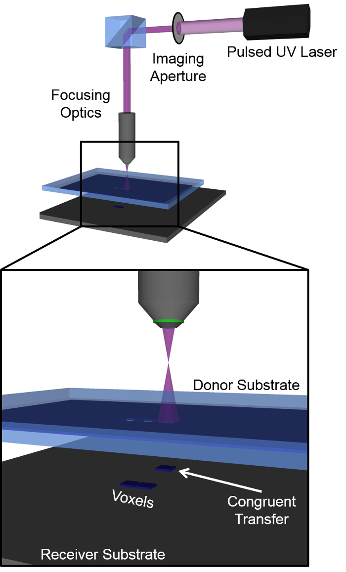
Figure 1. Schematic diagram of LDT setup. Note that the voxel shape is determined by the cross-sectional beam shape only for high-viscosity ink. Please click here to view a larger version of this figure.
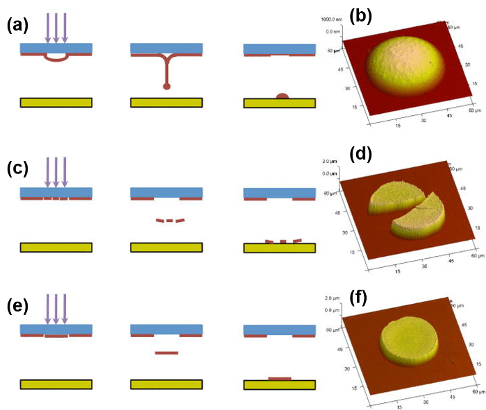
Figure 2. Schematic diagram voxel ejection. Diagrams illustrate evolution of transfer for (A) low viscosity, (C) high viscosity, and (E) intermediate viscosity. AFM plots of the resultant voxels are provided in (B), (D), and (F), respectively. This figure has been modified from [9]. Please click here to view a larger version of this figure.
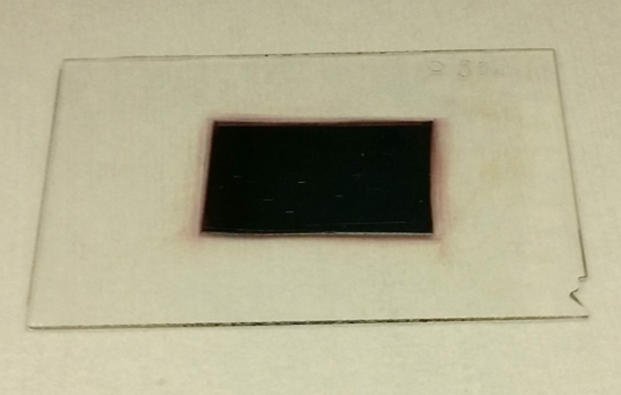
Figure 3. Picture of Ag nanopaste donor substrate. The substrate itself is a glass slide with a 1 µm deep well in the center. Please click here to view a larger version of this figure.
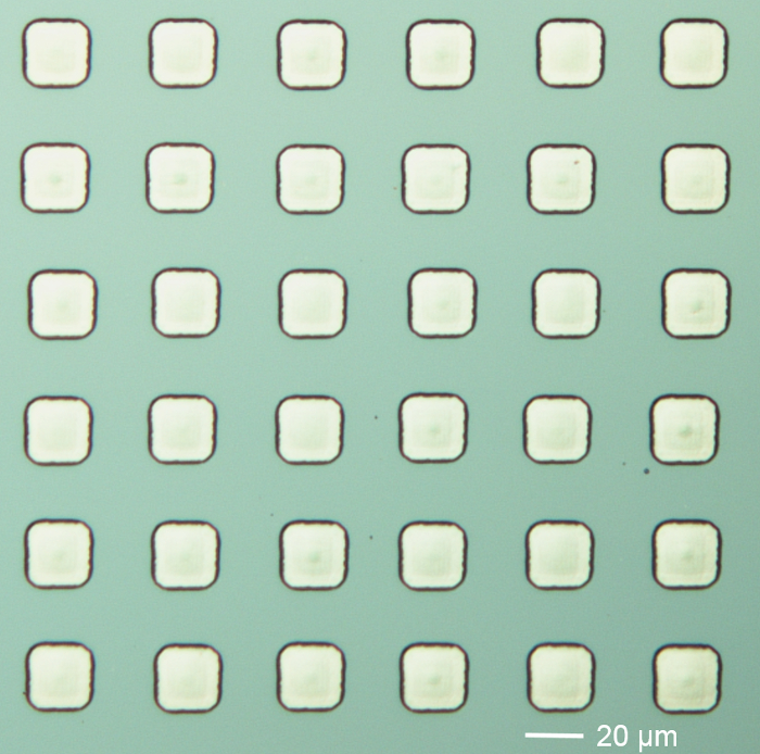
Figure 4. 20X optical image of the paste layer on the ribbon (donor substrate) after voxel transfer. Sharp, well-defined edges and lack of residue indicate sufficient paste drying and complete transfer of material from the ribbon. Please click here to view a larger version of this figure.
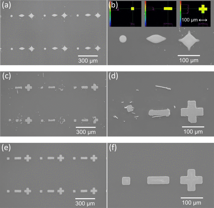
Figure 5. Scanning electron microscopy (SEM) images of several different voxels. Beam profiles are depicted in the inset (B). Three different voxel shapes were printed from low viscosity (A,B), high viscosity (C,D), and intermediate viscosity (E,F). Note that low viscosity leads to a loss of shape and voxel sharpness while high viscosity leads to voxel fracturing. This figure has been modified from [9]. Please click here to view a larger version of this figure.
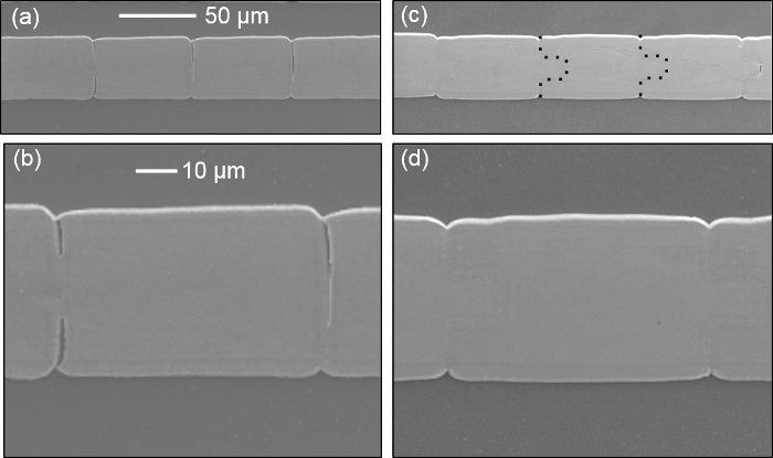
Figure 6. SEM images of conjoined voxel chains. Two linking geometries are depicted: simple end-to-end (A,B) and notched-interlocking (C,D). In general, notched-interlocking geometries are found to be more reliable while simple end-to-end have a tendency to crack due to shrinkage during the furnace steps. This figure has been modified from [20]. Please click here to view a larger version of this figure.
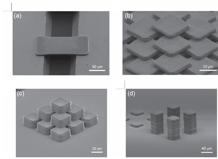
Figure 7. SEM images of multiple complex voxel structures. Geometries include: A rectangular voxel bridging a 100 µm wide trench (A), a multilayer scaffold (B), a high aspect ratio pyramid (C), and several high aspect ratio micro pillars (D). This figure has been modified from [8]. Please click here to view a larger version of this figure.
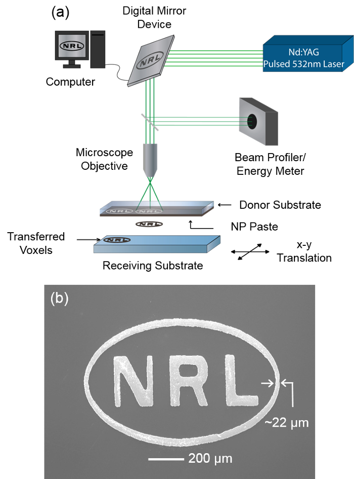
Figure 8. Schematic diagram and results of LDT via DMD chip. In the schematic diagram (A), the laser aperture has been replaced with the DMD chip, which is a large assembly of micro-mirrors. The pattern from an image file can be faithfully imaged onto the donor substrate, ejecting an exact replica of the pattern of voxels in a single shot. As an example, an NRL logo (B) has been transferred by a single laser shot. Please click here to view a larger version of this figure.
Discussion
In this paper, we have demonstrated a process for non-contact, three-dimensional printing as well as single-laser-shot, large area printing (via DMD chip) of high-viscosity Ag nanopaste. Unlike other direct-write techniques, such as inkjet, the LDT technique described here allows for the printing of complex voxel shapes with one laser pulse, i.e., in one single step. While many aspects of the procedure may seem straightforward, there are multiple steps that require iterative testing in order to optimize. First, paste dryness and viscosity are the most important factors for successful transfer. Although these points have been already been emphasized repeatedly in the text, we reiterate the point here to underline the importance. If the ink viscosity is too low, then it will be impossible to print sharp, well-defined voxel shapes. A telltale sign that the ink viscosity is too low occurs when attempting to eject a voxel. When the laser pulse is fired, the voxel will appear to momentarily eject, but the ink will fill back quickly in the hole left in the donor substrate. In this case, the user should stop firing the laser and the ink should be further treated as outlined in steps 3.1 and 3.2. If the ink viscosity is too high, the voxel transfer process will appear successful on the ribbon. However, when examining the voxels on the receiver substrate, there will be significant tearing, fracturing, or debris. In this case, the user needs to dispose of the current ribbon and make a new ribbon as outlined in section 2. Optimization of ink viscosity and drying time should be accomplished by evaluating the quality of voxel transfer attempts. We do not recommend trying to measure the viscosity of the paste at any point. Second, the laser fluence is almost as important as ink viscosity and very small changes in fluence can have a significant effect on the process. It should be very clear when the energy is too low — the voxel will not eject from the donor substrate. It is recommended to begin with the fluence range suggested in step 4.4, and then very incrementally increase the value. The lowest energy that results in a full transfer is called the "threshold fluence". It is often best to operate at or near the threshold fluence because higher fluence values will tend to fracture or tear the voxels. Finally, depending on the variety of laser used for the process, there could be hot spots in the laser profile. This may require an adjustment of the aperture to sample a more homogeneous region of the beam. If the shape of the ejected voxel is warped or poorly matches the shape of the beam cross section, laser hotspots or ink layer thickness or uniformity could be responsible.
Beyond troubleshooting, there are a few limitations to the technique. The final furnace curing step makes it difficult or impossible to achieve voxels with the desired functional properties on non-high-temperature compatible substrates. Generally, the Ag nanopaste used in this manuscript requires a curing temperature of at least 150 °C in order to obtain reasonable conductivity values. The fabrication of the ink layer on the donor substrate needs to be further optimized to improve thickness uniformity, areal coverage and processing time. The ink layer thickness has a dramatic effect on the threshold fluence and transfer quality, and inhomogeneous thickness can make the transfer process difficult, especially when transferring voxels smaller than 20 µm x 20 µm. The current design for the donor substrate makes it difficult to create ribbons larger than 10s of cm, which limits large-area throughput. Thus, the development of alternate donor substrate designs, such as reel-to-reel or rotating disc, would be required for enhanced automation and larger area processing.
The strength of the LDT technique lies in the ability to transfer fluids with high viscosities that other drop-on-demand techniques cannot handle. The advantages of LDT can be separated into two situations where firstly, printing high viscosity paste offers an improvement in quality or speed over printing low viscosity paste and secondly, in situations where printing with high viscosity paste enables structures that are not accessible to low viscosity printing. Examples of advantages in the first category are: minimal voxel variability from wetting effects, high degree of control over voxel shape and size, minimal shrinkage during curing, and low laser energy compared to other LIFT processes (and thus low transfer velocity). Examples in the second category are: printing of high-aspect-ratio structures, bridging structures, cantilevers, and any other structure that requires good voxel-shape-retention. By combining the LDT process with the DMD chip, parallel printing of complex shapes and patterns is enabled, which greatly speeds up the overall process. Furthermore, the use of a DMD to shape the voxels allows designs to be updated between laser pulses, enabling rapid printing of dynamically reconfigurable voxels. Generally speaking, the refresh rate of the DMD (33 kHz) is slightly slower than the max repetition rate of the laser (100 kHz or higher), but the rate limiting factor for printing speed is the stage translation.
The primary avenues for advancement with the LDT system are the continued development of additional materials, improving the ribbon fabrication process, and continuing to scale up the process through integrating digital light processing (DLP) technology such as the DMD chip. Although metallic and insulating materials have been successfully transferred through this process, few active materials have been developed. The ability to print piezoelectric, magnetic, or optoelectronic materials with the LDT process could open up enormous technological possibilities. As it stands, the geometry of the donor substrate limits scalability. The development of reel-to-reel or rotating disc donor substrates would streamline the processes considerably. Finally, combination of LDT with DLP technology is a potentially disruptive development for the field of digital fabrication, turning a previously serial process into a highly parallel process. A key challenge toward this goal is the ability to print voxels with good feature resolution at multiple scales. That is to say, voxels with lateral dimensions on the order of 10 sec or 100 sec of µm containing features on the order of 1-5 µm. Taken together, these developments offer significant opportunities for large-area additive manufacturing of electronic components.
Disclosures
The authors have nothing to disclose.
Acknowledgements
This work was funded by the Office of Naval Research (ONR) through the Naval Research Laboratory Basic Research Program.
Materials
| Name | Company | Catalog Number | Comments |
|---|---|---|---|
| Silver Nano-paste for Screen Printing | Harima Chemicals Group, http://www.harima.co.jp/en/ | NPS Type HP | Store at 10 °C, do not allow to freeze; before using, wait 1 hour for paste to reach room temperature. |
| Buffered HF Solution | http://transene.com/sio2/ | BUFFER HF IMPROVED | Etch rate may vary depending on material structure |
References
- Park, J. U., et al. High-resolution electrohydrodynamic jet printing. Nature Mater. 6, 782-789 (2007).
- Hon, K. K. B., Li, L., Hutchings, I. M. Direct writing technology - Advances and developments. CIRP Ann. 57, 601-620 (2008).
- Calvert, P. Inkjet Printing for Materials and Devices. Chem. Mater. 13, 3299-3305 (2001).
- Arnold, C. B., Serra, P., Piqué, A. Laser direct-write techniques for printing of complex materials. MRS Bulletin. 32, 23-31 (2007).
- Park, J. U., et al. High-resolution electrohydrodynamic jet printing. Nature Mater. 6, 782-789 (2007).
- Hon, K. K. B., Li, L., Hutchings, I. M. Direct writing technology - Advances and developments. CIRP Ann. 57, 601-620 (2008).
- Calvert, P. Inkjet Printing for Materials and Devices. Chem. Mater. 13, 3299-3305 (2001).
- Arnold, C. B., Serra, P., Piqué, A. Laser direct-write techniques for printing of complex materials. MRS Bulletin. 32, 23-31 (2007).
- Piqué, A., Auyeung, R. C. Y., Kim, H. K., Metkus, M., Mathews, S. A. Digital microfabrication by laser decal transfer. J. Laser. Micro. Nanoeng. 3, 163-168 (2008).
- Auyeung, R. C. Y., Kim, H., Birnbaum, A. J., Zalalutdinov, M., Mathews, S. A., Piqué, A. Laser decal transfer of freestanding microcantilevers and microbridges. Appl. Phys. A. 97, 513-519 (2009).
- Kim, H., Melinger, J. S., Khachatrian, A., Charipar, N. A., Auyeung, R. C. Y., Piqué, A. Fabrication of terahertz metamaterials by laser printing. Opt. Lett. 35, 4039-4041 (2010).
- Wang, J., Auyeung, R. C. Y., Kim, H., Charipar, N. A., Piqué, A. Three-dimensional printing of interconnects by laser direct-write of silver nanopastes. Adv. Mater. 22, 4462-4466 (2010).
- Mathews, S. A., Auyeung, R. C. Y., Kim, H., Charipar, N. A., Piqué, A. High-speed video study of laser-induced forward transfer of silver nano-suspensions. J. Appl. Phys. 114, 064910(2013).
- King, B. H., Dimos, D., Yang, P., Morissette, S. L. Direct-write fabrication of integrated, multilayer ceramic components. J. Electroceram. 3, 173-178 (1999).
- Lewis, J. A. Direct ink writing of 3D functional materials. Adv. Funct. Mater. 16, 2193-2204 (2006).
- Calvert, P. Inkjet printing for materials and devices. Chem. Mater. 13, 3299-3305 (2001).
- Kang, H., Soltman, D., Subramanian, V. Hydrostatic Optimization of Inkjet-Printed Films. Langmuir. 26, 11568-11573 (2010).
- Piqué, A., et al. Laser decal transfer of electronic materials with thin film characteristics. Proc. SPIE. 6879, 687911(2008).
- Auyeung, R. C. Y., Kim, H., Birnbaum, A. J., Zalalutdinov, M., Mathews, S. A., Piqué, A. Laser decal transfer of freestanding microcantilevers and microbridges. Appl. Phys. A: Mater. Sci. Process. 97, 513-519 (2009).
- Soltman, D., Smith, V., Kang, H., Morris, S. J. S., Subramanian, V. Methodology for inkjet printing of partially wetting films. Langmuir. 26, 15686-15693 (2010).
- Auyeung, R. C. Y., Kim, H., Charipar, N., Birnbaum, A., Mathews, S., Piqué, A. Laser forward transfer based on a spatial light modulator. Appl. Phys. A: Mater. Sci. Process. 102, 21-26 (2011).
- Duocastella, M., Fernandez-Pradas, J. M., Serra, P., Morenza, J. L. Jet formation in the laser forward transfer of liquids. Appl. Phys. A: Mater. Sci. Process. 93, 453-456 (2008).
- Feinaueugle, M., Alloncle, A. P., Delaporte, P., Sones, C. L., Eason, R. W. Time-resolved shadowgraph imaging of femtosecond laser-induced forward transfer of solid materials. Appl. Surf. Science. 258, 8475-8483 (2012).
- Breckenfeld, E., Kim, H., Auyeung, R. C. Y., Charipar, N., Serra, P., Piqué, A. Laser-induced forward transfer of silver nanopaste for microwave interconnects, A. Appl. Surf. Science. 331, 254-261 (2015).
Reprints and Permissions
