A method for electrochemically etching field emission tips is presented. Etching parameters are characterized and the operation of the tips in field emission mode is investigated.
A subscription to JoVE is required to view this content. Sign in or start your free trial.
Method Article
Electrochemical Etching and Characterization of Sharp Field Emission Points for Electron Impact Ionization
In This Article
Summary
Abstract
A new variation of the drop-off method for fabricating field emission points by electrochemically etching tungsten rods in a NaOH solution is described. The results of studies in which the etching current and the molarity of the NaOH solution used in the etching process were varied are presented. The investigation of the geometry of the tips, by imaging them with a scanning electron microscope, and by operating them in field emission mode is also described. The field emission tips produced are intended to be used as an electron beam source for ion production via electron impact ionization of background gas or vapor in Penning trap mass spectrometry applications.
Introduction
Sharp tips or points have long been used in microscopy applications, such as the field ion microscope (FIM)1 and the scanning tunneling microscope (STM)2, and a range of techniques for producing sharp tips of various materials have been developed3. These sharp tips can also be operated as field emission points (FEPs) by applying a high voltage to them, and serve as a convenient electron beam source. One application of such as source is ion production via electron impact ionization (EII). The FEP is particularly advantageous in applications where temperature fluctuations produced by thermal emitters are undesirable. For example, ion production via EII of background gas or vapor in high precision Penning traps4,5.
A simple method for fabricating FEPs is to electrochemically etch tungsten rods in a sodium hydroxide (NaOH) solution. This technique is relatively straightforward to implement with modest equipment and has been shown to be quite reproducible and reliable. A number of methods are described in the literature and improvements to these techniques continue to appear6. Here we describe a method for the electrochemical etching of tungsten tips in a NaOH solution. Our method is a variation of the lamella drop-off technique7,8 and the floating layer technique9,10. Like these two methods it enables the production of two tips from a single etching procedure. A picture of the experimental apparatus for etching the tips is shown in Figure 1.
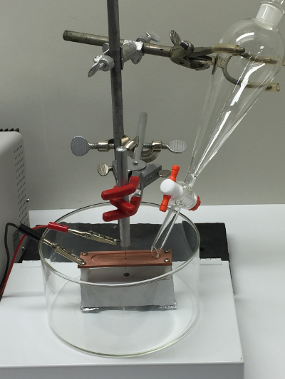
Figure 1. Etching apparatus. Photograph of the experimental apparatus used for electrochemical etching of tungsten rods with NaOH solution. Please click here to view a larger version of this figure.
Electrochemical etching of tungsten in the aqueous NaOH base occurs via a two-stage process. First, intermediate tungsten oxides are formed, and second, these oxides are non-electrochemically dissolved to form the soluble tungstate anion. This process is described, in simplified form, by the two reactions
(1) W + 6OH- → WO3(S) + 3H2O + 6e-, and
(2) WO3(S) + 2OH- → WO42- + H2O.
The etching current and the NaOH solution molarity used affect the time and voltage required to etch through the tungsten rod. Studies of these effects are presented and discussed. More importantly, the etching parameters have an effect on the geometry of the tips and, as such, on their operation in field emission mode. The geometry of the tips we produced were characterized by imaging them with a scanning electron microscope (SEM). These images can be used to estimate, for example, the tip radius. In addition, the tips were operated in field emission mode by applying a negative voltage of typically a few hundred volts to a few kilovolts to them and monitoring the resulting electron emission current. The relationship between field emission current, I, and applied bias voltage, V, can be described by the Fowler-Nordheim equation11
(3) I = AV2 e-Creff/V,
where reff is the effective radius of the tip, A is a constant, and C is the second Fowler-Nordheim constant  , in which b = 6.83 eV-3/2V/nm,
  is the work function of tungsten ( ≈ 4.5 eV), k is a factor that depends on geometry (k ≈ 5), and
  is the Nordheim image correction term ( ≈ 1)12. Hence, the effective radius of the tip can be determined by measuring the electron current as a function of bias voltage. Specifically, it can be obtained from the slope of a so-called Fowler-Nordheim (FN) plot of ln(I/V2) vs 1/V.
Access restricted. Please log in or start a trial to view this content.
Protocol
1. Electrochemical Etching
- Experimental set-up
- Apparatus
Note: The electrochemically etching set-up requires a standard 0 - 30 V direct current (DC) benchtop power supply and appropriate cables, a separatory funnel, a wide base glass beaker, and standard rod and utility clamp with electrically insulating grips. Small screws, insulated stand-offs, and alligator clips will also be required. Additional items, described below and shown in the picture of the etching apparatus in Figure 1, must be fabricated.- Make a tungsten rod holder from an approximately 100 mm long 6 mm diameter aluminum rod. Drill a 0.5 mm diameter approximately 8 mm deep hole in the center, and make a tapped hole for a 4-40 screw in the side to hold the rod in place.
- Make a counter electrode from an approximately 100 mm x 30 mm x 3 mm thick copper plate with an approximately 75 mm x 20 mm x 1.5 mm deep reservoir milled into it, and a 1.5 mm diameter hole in the center. Attach approximately 15 mm long insulated stand-offs to the backside of the counter electrode.
- Make an FEP catcher by drilling a 6 mm diameter 8 mm deep hole into an approximately 75 x 20 x 20 mm copper block.
- Preparation of tungsten rod
- Use wire clippers to cut the 0.5 mm diameter tungsten rods into approximately 25 mm lengths.
- Clean the rods in acetone in an ultrasonic bath for 15 min.
- Rinse the rods with deionized water.
- Etching solution
Caution: NaOH solution is a corrosive alkali solution-NFPA 704 label: Flammability (0), Health (3), Instability/Reactivity (0), Special (COR)-and can cause chemical burns if it comes in contact with the skin or eyes. Inhalation of fumes can cause irritation and burns to the respiratory tract. When handling NaOH solution, wear chemical splash goggles and face shield to protect the eyes, and gloves and an apron to protect the skin. Perform the etching procedure in a fume hood or wear a respirator. Care should be taken when performing step 1.1.3.1 to produce the diluted NaOH solution. This process is highly exothermic and can release heat that may cause burns or ignite flammables, and could cause the solution to splash out of the container.- Make a 1.5 M NaOH solution by combining 30 ml of 50% by weight NaOH solution with 370 ml of deionized water to make a 400 ml total volume.
- Fill a separatory funnel with the NaOH solution.
- Cut-off circuit
Note: If the DC power supply is to be operated manually, then the operator will turn the power supply off once the tungsten rod has etched all the way through (see 1.2.2). In case of manual operation, skip to step 1.2. For automatic cut-off of the DC power supply, the cut-off circuit (shown in Figure 2 and described below), should be constructed. Here, we implement the computer control using a DAQ card.- Connect an ammeter in series with the DC power supply.
- Connect two resistors, R1 and R2 in series and place in parallel with the tungsten rod/counter electrode etching leg of the circuit. (Nominal values for R1 and R2 are R1 = 5 kΩ and R2 = 10 kΩ.)
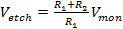
- Monitor the voltage across one of the resistors with an analog-to-digital convertor (ADC) and suitable computer control software, e.g., LabVIEW. The monitored voltage, Vmon, can be related to the voltage across both resistors and hence, the voltage across the etching leg, Vetch, via
(4) ,
,
where the voltage is being monitored across R1. - Connect a low resistance resistor, RL = 1 Ω, in series in the etching circuit. Use a second channel on the ADC to record the voltage across this resistor. The etching current is then found via ietch ≈ VL/RL. (Only about 1 mA flows throw the monitor leg of the circuit.)
- In software, create a program to output a 5 V TTL signal from the digital input/output channel (DI/O) when either the etching voltage increases above a set-value, or the etching current drops below a set value, indicating that the tungsten rod has etched all the way through. These values depend on the etching current and NaOH solution molarity being used and should be determined with a test run of the experiment.
- As shown in Figure 2, arrange for the 5 V TTL signal to open a relay to stop the current flow.
- Apparatus
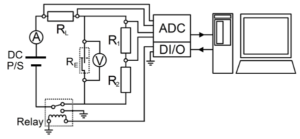
Figure 2. Schematic of etching circuit. A schematic drawing of the etching circuit used to provide the constant DC etching current. The current is determined by monitoring the voltage across a low resistance resistor and the voltage is recorded by monitoring the voltage across a high resistance resistor using an ADC. A computer program monitors the current and provides a 5 V output signal to a relay that opens the etching circuit once the current drops below a specified value. Please click here to view a larger version of this figure.
- Etching procedure
- Apparatus preparation
- Set up the apparatus as shown in Figure 1, with the copper FEP catcher block placed inside the wide base glass beaker and the copper cathode located above it, spaced off by the insulating stand-offs.
- Set the current on the DC power supply to the desired value, typically 200 mA.
- Place a tungsten rod in the holder and connect the positive terminal of the DC power supply to the 4-40 holding screw with an alligator clip.
- Insert the tungsten rod through the hole in the copper cathode so that approximately 12 mm of the tungsten rod passes through the hole.
- Connect the negative terminal of the power supply to the copper cathode with another alligator clip.
- Etching
- Manually adjust the drip rate of the separatory funnel to match the drip rate through the hole, about 1 drip every 3 sec. Wait for the reservoir in the copper cathode to become full.
- Turn on the DC power supply to begin etching.
- If operating in manual mode, turn off the DC power supply once the bottom part of the tip etches all the way through and drops off. If operating with an automatic shut-off switch, the etching current will be cut-off automatically once the rod etches through.
- Apparatus preparation
2. Characterization of Field Emission Points
- Inspection of tips
- Carefully remove the bottom tip from the catcher block using pliers or tweezers. Remove the upper tip from the tungsten rod holder by loosening the 4-40 screw and gently pulling the upper tip out with the pliers or tweezers.
- Rinse with acetone and then with deionized water.
- Examine with an optical microscope. Tips should be seen to taper to a fine point. Those that do not, e.g., because they are bent or do not have a regular cone structure, should be discarded. Figure 3 shows an example of (a) a good tip and (b) a bent tip.
- Store tips in a desiccator.

Figure 3. Optical image of FEP tips. Picture of (a) a good tip and (b) a bad tip, as viewed through an optical microscope. Please click here to view a larger version of this figure.
- Scanning Electron Microscope (SEM) Imaging
- For SEM Imaging, secure FEP tips to a conducting holder using conducting tape or by screwing them to it (e.g., see Figure 4) and image in a SEM according to manufacturer's protocol at magnifications of approximately 1,800X and 37,000X to view the cone of the tip and the end of the tip, respectively.

Figure 4. FEP holder for SEM imaging. A picture of (a) the top and (b) the bottom of the holder used to secure FEPs while imaging with the SEM. Please click here to view a larger version of this figure.
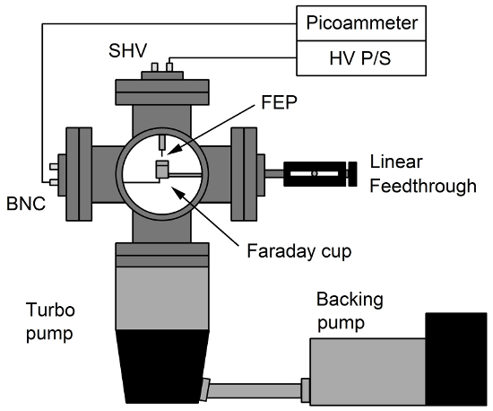
Figure 5. Field emission apparatus. Schematic of the apparatus used to apply a HV to the FEPs while under vacuum to produce an electron beam. The electron beam current is monitored on the Faraday cup with a picoammeter. Please click here to view a larger version of this figure.
- Field Emission Tests
- Apparatus
Note: For the field emission tests the following, or similar, equipment is required: a 6-way 6" conflat flange cross to serve as a vacuum chamber, three 6" to 2 ¾" conflat flange zero length adaptors, an SHV (safe high voltage) feedthrough on a 2 ¾" conflat flange, a BNC feedthrough on a 2 ¾" conflat flange, a linear feedthrough on a 2 ¾" conflat flange, a 6" conflat flange window, a 6" conflat flange blank off, a turbo vacuum pump mounted to a 6" conflat flange, and a backing pump (e.g., a scroll pump) for the turbo. A high voltage (HV) power supply capable of delivering up to -5 kV is required to bias the FEP, and a picoammeter is required to monitor the electron current emitted from the FEP and collected on a Faraday cup, see e.g., 13. In lieu of a Faraday cup, a simple conducting collection plate can be used. A schematic of the field emission set-up is shown in Figure 5.- Make a second tungsten rod holder (see step 1.1.1.1). In the opposite end of the holder to the FEP drill a 1 mm diameter hole and drill and tap a hole in the side of the rod for a 4-40 screw to secure it to the vacuum side of the SHV feedthrough.
- Set-up the field emission apparatus as shown in Figure 5. The Faraday cup should be about 2 cm from the end of the FEP.
- Connect the HV supply to the SHV feedthrough that the FEP holder is attached to, and connect the picoammeter to the BNC feedthrough that the Faraday cup is attached to.
- Pump down the set-up to a pressure of 10-6 mbar or below.
- Field emission
- Gradually increase the bias on the FEP and monitor the electron beam current on the Faraday cup with a picoammeter. When field emission begins, a current will be observed on the picoammeter.
- Increase the HV in incremental steps (of around 50 V) and record the average electron beam current on the picoammeter at each step. (This process can be computer controlled e.g., by a LabVIEW program if desired, or can be done manually). Keep the electron beam current below 1 μA.
- Conditioning
- Condition the tip by operating in field emission mode at 5 nA for 1 hr.
- Repeat the current vs HV scan of 2.3.2.2.
- Apparatus
Access restricted. Please log in or start a trial to view this content.
Results
Study of etching parameters
During the etching process the power supply is operated in constant current mode. The voltage required to maintain this constant current increases slightly as the tungsten rod is etched away (due to the increase in resistance of the rod). The current drops almost to zero when the tip etches all the way through. A small current continues to flow due to the fact that the upper tip is st...
Access restricted. Please log in or start a trial to view this content.
Discussion
We have described straightforward procedures to electrochemically etch sharp field emission points (FEPs) in a NaOH solution, and to test the FEPs by operating them in field emission mode. The etching procedure described is a variation of existing techniques-the lamella drop-off technique7,8 and the floating layer technique9,10. However, we found it to be more convenient and reliable to implement than the aforementioned methods.
Before starting the etching procedure, to m...
Access restricted. Please log in or start a trial to view this content.
Disclosures
The authors have nothing to disclose.
Acknowledgements
We acknowledge the services of Stanley Flegler, Carol Flegler, and Abigail Tirrell at the MSU Center for Advanced Microscopy. We thank Ray Clark and Mark Wilson for technical assistance with the set-up of the electrochemical etching apparatus. Earlier contributions from Anne Benjamin, Georg Bollen, Rafael Ferrer, David Lincoln, Stefan Schwarz and Adrian Valverde, and technical assistance from John Yurkon are also acknowledged. This work was partially supported by the National Science Foundation contract no. PHY-1102511 and PHY-1307233, Michigan State University and the Facility for Rare Isotope Beams, and Central Michigan University.
Access restricted. Please log in or start a trial to view this content.
Materials
| Name | Company | Catalog Number | Comments |
|---|---|---|---|
| Tungsten Rod 0.020" x 12" | ESPI Metals | http://www.espimetals.com/index.php/online-catalog/467-Tungsten | 3N8 Purity |
| 50% by weight NaOH solution | Sigma-Aldrich | 415413-500ML | 500 ml |
| Separatory funnel | Cole-Parmer | Item# WU-34506-03 | 250 ml |
| DC Power supply | BK Precision | 1672 | Triple Output 0 - 32 V, 0 - 3 A DC Power Supply |
| Acetone | Cole-Parmer | Item# WU-88000-68 | 500 ml |
| Data Acquisition Card | National Instruments | NI PXI-6221 | 16 AI, 24 DIO, 2 AO |
| Relay | Magnecraft | 276 XAXH-5D | 7 A, 30 V DC Reed Relay |
| 6-way 6" conflat flange cross | Kurt J Lesker | C6-0600 | |
| 6" to 2-3/4" conflat zero length reducer flange (x3) | Kurt J Lesker | RF600X275 | |
| 2-3/4" conflat flange SHV feedthrough | Kurt J Lesker | IFTSG041033 | |
| 2-3/4" conflat flange BNC feedthrough | Kurt J Lesker | IFTBG042033 | |
| 2-3/4" conflat flange linear feedthrough | MDC | 660006, REF# BLM-275-2 | |
| 6" conflat flange blankoff | Kurt J Lesker | F0600X000N | |
| 6" conflat flange window | Kurt J Lesker | VPZL-600 | |
| HV Power supply | Keithley Instruments | Keithley Model #2290-5 | 0 - 5 kV DC HV Power Supply |
| Picoammeter | Keithley Instruments | Keithley Model #6485 | |
| Faraday Cup | Beam Imaging Solutions | Model FC-1 Faraday Cup |
References
- Muller, E. W., Bahadur, K. Field Ionization of Gases at a Metal Surface and the Resolution of the Field Ion Microscope. Phys. Rev. 102, 624(1956).
- Binnig, G., Rohrer, H. Scanning Tunneling Microscopy. Helv. Phys. Acta. 55, 726-735 (1982).
- Melmed, A. J. The art and science and other aspects of making sharp tips. J. Vac. Sci. Technol. B. 9, 601-608 (1990).
- Shi, W., Redshaw, M., Myers, E. G. Atomic masses of 32,33S, 84,86Kr, and 129,132Xe with uncertainties 0.1 ppb. Phys. Rev. A. 72, 022510(2005).
- Van Dyck, R. S. Jr, Zafonte, S. L., Van Liew, S., Pinegar, D. B., Schwinberg, D. B. Ultraprecise Atomic Mass Measurement of the α particle and 4He. Phys. Rev. Lett. 92, 220802(2004).
- Hobara, R., Yoshimoto, S., Hasegawa, S., Sakamoto, K. Dynamic electrochemical-etching technique for tungsten tips suitable for multi-tip scanning tunneling microscopes. e-J. Surf. Sci. Nanotechnol. 5, 94-98 (2007).
- Klein, M., Schwitzgebel, G. An improved lamellae drop-off technique for sharp tip preparation in scanning tunneling microscopy. Rev. Sci. Instrum. 68, 3099-3103 (1997).
- Kerfriden, S., Nahlé, A. H., Campbell, S. A., Walsh, F. C., Smith, J. R. The electrochemical etching of tungsten STM tips. Electrochim. Acta. 43, 1939-1944 (1998).
- Lemke, H., Göddenhenrich, T., Bochem, H. P., Hartmann, U., Heiden, C. Improved microtips for scanning probe microscopy. Rev. Sci. Instrum. 61, 2538-2538 (1990).
- Song, J. P., Pryds, N. H., Glejbøl, K., Mørch, K. A., Thölén, A. R., Christensen, L. N. A development in the preparation of sharp scanning tunneling microscopy tips. Rev. Sci. Instrum. 64, 900-903 (1993).
- Fowler, R. H., Nordheim, L. Electron Emission in Intense Electric Fields. Proc. R. Soc. Lond. A. , 119-173 (1928).
- Kim, Y. -G., Choi, E. -H., Kang, S. -O., Cho, G. Computer-controlled fabrication of ultra-sharp tungsten tips. J. Vac. Sci. Technol. B. 16, 2079(1998).
- Brown, K. L., Tautfest, G. W. Faraday-Cup Monitors for High-Energy Electron Beams. Rev. Sci. Instrum. 27, 696(1956).
- Redshaw, M., et al. Fabrication and characterization of field emission points for ion production in Penning trap applications. Int. J. Mass Spectrom. 379, 187-193 (2015).
- Ibe, J. P., et al. On the electrochemical etching of tips for scanning tunneling microscopy. J. Vac. Sci. Technol. A. 8, 3570(1990).
- Ekvall, I., Wahlström, E., Claesson, D., Olin, H., Olsson, E. Preparation and characterization of electrochemically etched W tips for STM. Meas. Sci. Technol. 10, 11-18 (1999).
- Schiller, C., Koomans, A. A., van Rooy, T. L., Schönenberger, C., Elswijk, H. B. Decapitation of tungsten field emitter tips during sputter sharpening. Surf. Sci. 339, L925-L930 (1995).
Access restricted. Please log in or start a trial to view this content.
Reprints and Permissions
