Uniformly sized nanoparticles can remove fluctuations in contact hole dimensions patterned in poly(methyl methacrylate) (PMMA) photoresist films by electron beam (E-beam) lithography. The process involves electrostatic funneling to center and deposit nanoparticles in contact holes, followed by photoresist reflow and plasma- and wet-etching steps.
A subscription to JoVE is required to view this content. Sign in or start your free trial.
Method Article
Use of Sacrificial Nanoparticles to Remove the Effects of Shot-noise in Contact Holes Fabricated by E-beam Lithography
In This Article
Summary
Abstract
Nano-patterns fabricated with extreme ultraviolet (EUV) or electron-beam (E-beam) lithography exhibit unexpected variations in size. This variation has been attributed to statistical fluctuations in the number of photons/electrons arriving at a given nano-region arising from shot-noise (SN). The SN varies inversely to the square root of a number of photons/electrons. For a fixed dosage, the SN is larger in EUV and E-beam lithographies than for traditional (193 nm) optical lithography. Bottom-up and top-down patterning approaches are combined to minimize the effects of shot noise in nano-hole patterning. Specifically, an amino-silane surfactant self-assembles on a silicon wafer that is subsequently spin-coated with a 100 nm film of a PMMA-based E-beam photoresist. Exposure to the E-beam and the subsequent development uncover the underlying surfactant film at the bottoms of the holes. Dipping the wafer in a suspension of negatively charged, citrate-capped, 20 nm gold nanoparticles (GNP) deposits one particle per hole. The exposed positively charged surfactant film in the hole electrostatically funnels the negatively charged nanoparticle to the center of an exposed hole, which permanently fixes the positional registry. Next, by heating near the glass transition temperature of the photoresist polymer, the photoresist film reflows and engulfs the nanoparticles. This process erases the holes affected by SN but leaves the deposited GNPs locked in place by strong electrostatic binding. Treatment with oxygen plasma exposes the GNPs by etching a thin layer of the photoresist. Wet-etching the exposed GNPs with a solution of I2/KI yields uniform holes located at the center of indentations patterned by E-beam lithography. The experiments presented show that the approach reduces the variation in the size of the holes caused by SN from 35% to below 10%. The method extends the patterning limits of transistor contact holes to below 20 nm.
Introduction
The exponential growth in computational power, as quantified by Moore's law1,2 (1), is a result of progressive advances in optical lithography. In this top-down patterning technique, the achievable resolution, R, is given by the well-known Raleigh theorem3:

Here, λ and NA are the light wavelength and numerical aperture, respectively. Note that NA = η·sinθ, where η is the refractive index of the medium between the lens and the wafer; θ = tan-1(d/2l) for the diameter, d, of the lens, and the distance, l, between the center of the lens and the wafer. Over the last fifty years, the lithographic resolution has improved through the use of (a) light sources, including excimer lasers, with progressively smaller UV wavelengths; (b) clever optical designs employing phase-shift masks4; and (c) higher NA. For exposure in air (η = 1), NA is always less than unity, but by introducing a liquid with η >1, such as water5, between the lens and the wafer, NA can be elevated above 1, thereby improving the resolution of immersion lithography. Currently viable paths to a 20-nm node and beyond include extreme UV sources (λ = 13 nm) or patterning techniques using complex double and quadruple processing of a multilayered photoresist6,7.
At nanometer-length scales, statistical fluctuations, caused by shot-noise (SN), in the number of photons arriving within a nano-region cause variation in the dimensions of lithographic patterns. These effects are more pronounced with exposure to high-energy EUV light and E-beams, systems that need orders of magnitude fewer photons/particles compared to normal optical lithography8. Supersensitive chemically amplified (with a quantum efficiency >1) photoresists also introduce a chemical SN caused by a variation in the number of photoreactive molecules in exposed nanoregions9,10. Lower sensitivity photoresists that need longer exposures suppress these effects, but they also reduce throughput.
On the molecular scale, the contribution to line-edge roughness from the molecular size distribution inherent to the photoresist polymers may be reduced by using molecular resists11. An approach that is complementary to this top-down processing of nano-patterning is the use of bottom-up methods12,13 that rely specifically on the directed self-assembly (DSA) of diblock polymers14. The ability of these processes to direct nucleation and to create non-uniform spacing between desired patterns, such as holes or lines, remains challenging. The size distribution of molecular components15,16 also limits the scale and yield of fabrication17,18. Similar problems limit microcontact printing of nanoparticles in soft lithography19.
This paper presents studies of a new hybrid approach (Figure 1) that combines the classic top-down projection lithography with electrostatically directed self-assembly to reduce the effect of SN/line-edge roughness(LER)20. Positively charged amine groups on self-assembled monolayers (SAMs) of N-(2-aminoethyl)-11-amino-undecyl-methoxy-silane (AATMS) underlying the PMMA film are exposed after development. The negatively charged photoresist film of PMMA electrostatically funnels negatively charged gold nanoparticles (GNPs), capped with citrate,21-24 into SN-affected holes25. Re-flow of the PMMA photoresist engulfs predeposited nanoparticles in the film.
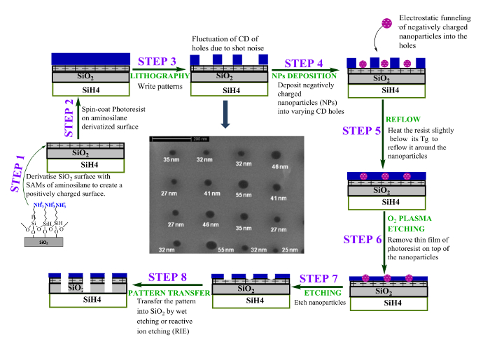
Figure 1: Schematic representation of the strategy to remove the effects of shot-noise and line-edge roughness for the patterning of contact holes using NPs of precise size. Here, the critical dimension (CD) is the desired diameter of the holes. The approach (step 1) begins with depositing a self-assembled monolayer (SAM) of silane molecule bearing positively charged amine groups on the oxide surface of a silicon wafer. Next, E-beam lithography is used to pattern the holes (steps 2 and 3) in PMMA photoresist film, the blue layer, which generates shot-noise, as illustrated in the inset SEM image. Lithography exposes amine groups at the bottom of the holes. Step 4 entails the aqueous phase deposition of controlled-size, citrate-capped (negatively charged) gold nanoparticles (GNPs) in lithographically patterned holes using electrostatic funneling (EF). In step 5, heating the wafer to 100 °C, below the glass transition temperature of the PMMA, 110 °C, causes the reflow of the photoresist around pre-deposited nanoparticles. Etching overlaid PMMA with oxygen plasma (step 6) exposes the GNPs, and subsequent wet-etching (iodine) of the exposed particles (step 7) creates holes corresponding to the size of the GNPs. When coupled with reactive-ion/wet-etching, it is possible to transfer the hole pattern in the photoresist to SiO2 (step 8)31. Reprinted with permission from reference20. Please click here to view a larger version of this figure.
The electrostatic interaction between the oppositely charged GNPs and amine groups on the substrate prevents the displacement of the GNPs from the binding site. The reflow step maintains the relative location of the GNPs but erases the holes and the effects of SN/LER. Plasma/wet etching steps regenerate holes that have the size of the GNP. Reactive-ion etching transfers their pattern to SiO2 hard-mask layers. The method relies on using more uniformly sized nanoparticles than a patterned nanohole (NH), expressed as the standard deviation, σ, such that σGNP <σNH. This report focuses on steps (4 and 5 described in Figure 1) involving the deposition of nanoparticles from dispersion and the reflow of the photoresist around them to assess the advantages and limitations of the method. Both steps are, in principle, scalable to larger substrates, requiring no extensive modification of the current flow of producing modern integrated circuits on chips.
Access restricted. Please log in or start a trial to view this content.
Protocol
1. Derivatize and Characterize the Surface of the Silicon Wafers
- Clean the surface of wafers using Radio Corporation of America (RCA) cleaning solutions SC1 and SC2.
- Prepare SC1 and SC2 by volumetrically mixing the following chemicals:
SC1: H2O2:NH4OH:H2O = 1:1:5 v/v and SC2: H2O2:HCl:H2O = 1:1:5 v/v.- Immerse the wafer in SC1 for 10 min at 70 °C, and then perform a deionized water wash.
- Follow a similar protocol for SC2 (10 min at 70 °C, followed by a wash).
NOTE: The cleaning procedure removes organic and ionic impurities and generates silanol groups on the silicon oxide surface of the silicon wafers.
- Derivatize the surfaces of the silicon wafers with AATMS
- Incubate the cleaned silicon wafer in 0.05 M AATMS (prepared in dry toluene) at 80 °C for 20 min. Sonicate for 5 min in a 100 W sonicator at room temperature in pure toluene for 5 min and dry in a stream of nitrogen gas.
- Characterize the surfaces of the derivatized silicon wafers
- Measure the contact angle using a goniometer and ImageJ software25.
- Determine the thickness of the films using an ellipsometer (He-Ne laser light source, λ = 632.8 nm, fixed incidence angle of 70°)25.
- Estimate the surface elemental composition by X-ray photoelectron spectroscopy (XPS)25.
2. E-beam Patterning
- Spin-coat photoresist (2% poly(methyl methacrylate (PMMA) in anisole) on AATMS- derivatized wafers at 4,000 rpm for 60 s.
- Prebake the film at 180 °C for 120 s to dry the photoresist film.
- Measure the photoresist film thickness using an ellipsometer. Ensure that the He-Ne laser light source, λ = 632.8 nm, is fixed at an incidence angle of 70°. Optimize the sample stage to maximize the detector signal using a reflective surface such as silicon wafer. Use the ellipsometer measurement program (GEMP) on the attached PC to measure the photoresist film thickness; it should be about 100 nm.
- E-beam exposure:
- Transfer the wafer to a high-vacuum chamber of an E-beam aligner.
- Create a poker dot hole pattern using an electron beam (30 kV accelerating voltage, 37 pA beam current) passing through a 10-µm aperture and providing a 24 µC/cm3 dosage.
- Adjust the pattern pitch and dosage as needed to produce a poker dot-type hole-pattern of the desired hole diameter (80 nm) and pitch (200 nm).
- Remove the wafer from the E-beam chamber.
- Develop the lithographic pattern:
- Begin pattern development in a solution of methyl isobutyl ketone/isopropyl alcohol (MIBK/IPA, 1:3 (v:v)) for 70 s.
- Continue to develop further by immersion in IPA for 30 s. Complete the development by washing in deionized water for 30 s. Dry the wafer in a stream of nitrogen gas.
3. Deposition of GNPs into E-beam-patterned Holes
NOTE: Deposition of GNPs in patterned holes employs two different methods.
- Immerse pre-patterned wafers in GNP solutions (Method 1).
- Leave the sample in the GNP suspension medium for 24-48 h, depending on the size of the GNP and the diameters of the holes. Use a 20-nm, citrate-capped GNP suspension containing 7.0 x 10¹¹ NPs/mL.
NOTE: One may employ a GNP size from 10-100 nm and a concentration range from 5.7 x 10¹² - 5.7 x 10⁹ NPs/mL, as provided by Ted Pella. Note that the deposition density obeys the diffusion law ̴(Dt)1/2, where D and t are diffusion coefficients of the nanoparticle and deposition time, respectively (i.e., smaller particles take a shorter time for deposition, as discussed in reference 20, Figure 2c).
- Leave the sample in the GNP suspension medium for 24-48 h, depending on the size of the GNP and the diameters of the holes. Use a 20-nm, citrate-capped GNP suspension containing 7.0 x 10¹¹ NPs/mL.
- Spray-deposit GNPs on the patterned wafers (Method 2)
- To deposit GNPs by evaporation, spray a solution of GNPs onto the patterned substrate, placed horizontally. Orient the hand-held sprayer (Method 2) so that the spray is directed perpendicularly to the substrate surface.
- Spray a sufficient volume of the suspension solution to wet the entire substrate surface.
NOTE: It may be necessary to dilute the GNP suspension by 10x to avoid forcing multiple nanoparticles into a large hole. - Incubate samples on a hot plate maintained at 30-35 °C to produce controlled evaporation for 10 min.
- After deposition (by either Method 1 or Method 2), mildly ultrasonicate (100 W) the samples in deionized water for 50 s and dry in a stream of nitrogen gas.
4. Scanning Electron Microscopy Imaging
NOTE: Two types of studies involved conventional top-down and cross-sectional SEM imaging.
- For top-down SEM images, use an E-beam accelerating voltage of 5 kV at a current of ~300 µA to prevent damage to the photoresist film.
Caution: The lowest possible voltage and current setting are necessary to reduce chain scission reactions in the photoresist. These chain scission reactions reduce the glass transition temperature of the polymer, which in turn affects the operational temperature for the resist reflow step described below. - Cross-section imaging:
- Sputter-coat 10 nm of thick gold film over PMMA photoresist to prevent ion-beam damage. Use a focused Ga ion beam operated at 30 kV and 93 pA to cut through the holes. Obtain cross-section SEM images by tilting the wafer from its normal horizontal position.
5. Reflow of PMMA Photoresist around GNPs in the Patterned Holes
- Heat the patterned substrates on a hot plate at Treflow (100 °C) for 3 min, which is below the pre-determined glass transition temperature, Tg (110 °C), of 950,000 g/mol PMMA; the rate of reflow for the polymer was 1.7 ± 0.1 nm/s.
Caution: Significantly faster reflow occurred for the patterned areas that had previously been exposed to the E-beam during imaging with scanning electron microscopy (SEM), perhaps because of the cleavage of the polymeric backbone chain during exposure to the electron beam, leading to a reduction of Tg. This observation is supported by the studies from Keymeulen and co-workers, who noted that exposure to X-ray radiation reduced the Tg of PMMA26.
6. Dry- and Wet-etch
- Dry-etch for sufficient duration (55 s) with oxygen-plasma to expose GNPs covered with a thin film of PMMA after reflow. Carefully monitor the rate of PMMA film etching as a function of time using an ellipsometer or thin film thickness monitor.
NOTE: A too-short etching duration may not expose the GNPs, while etching for too long would completely remove the PMMA film. For 950 kDa PMMA, the etch rate was 1.5 nm/s, necessitating 55 s of etching time. - Wet-etch GNPs at the bottom of the contact holes after reflow using a solution of iodine, containing 1.0 g of iodine crystal (I2), 4.0 g of potassium iodide (KI), and 40 mL of deionized water, for 10 min.
NOTE: Potassium iodide improves the solubility of the iodine in solution and facilitates gold etching. The reaction of gold with iodine (2Au + I2 → 2 AuI) produces gold iodide, which is slightly soluble in aqueous solution at room temperature.
7 . Calculation of Particle Displacement, Density, and Fill Fraction
- Locating the hole center and GNP displacement:
- By hand, draw horizontal and vertical best-fit straight lines through the rows and columns of holes, respectively, to established hole centers at the intersections of these lines (Figure 2a and 2b). Include at least 500+ holes in the calculations.
- Manually determine the position, r, of each nanoparticle relative to the center of the nanohole (i.e., the displacement) where it was deposited (Figure 2b).
- Determine the particle count versus displacement histograms using a standard spreadsheet program.
- Calculation of the particle density: ρ = N (Number of Particles)/Unit Area (µm2):
- First, determine the annular area of a ring with a fixed width (≈R/10, where R is the radius of the hole) and bounded by two radii (r1, r2) at a displacement of r (=(r1+r2)/2);
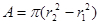 .
. - Sum the number of particles, N, in the area from the histogram constructed in step 7.2, above.
- Repeat the procedure as a function of r to generate about 10 equal steps terminating at r = R, the hole radius.
- First, determine the annular area of a ring with a fixed width (≈R/10, where R is the radius of the hole) and bounded by two radii (r1, r2) at a displacement of r (=(r1+r2)/2);
- Fit the particle density versus the displacement data to a Gaussian curve using a nonlinear least squares procedure (Figure 2a, inset)20. Extract the standard deviation of displacement (σdeposition) for the deposition and its fitting uncertainty.
- Repeat the above procedure for the SEM patterns obtained after the photoresist reflow using an SEM image shown in Figure 2c.
NOTE: After the reflow holes disappear, draw best-fit horizontal and vertical lines on GNP positions to determine the best-fit values for the hole centers. Calculate the particle displacements as in step 7.1 and extract the combined σTotal following the protocol delineated in steps 7.2-7.4.
NOTE: Here, combined or total refers to the overall displacement of GNP due to the deposition and reflow steps. - Determine the fill fraction by estimating the ratio of the number of filled holes to the total number of holes, Figure 2b.
Access restricted. Please log in or start a trial to view this content.
Results
Figure 2 shows an SEM image of 20-nm GNPs deposited in 80-nm diameter holes patterned in a 60-100 nm-thick PMMA film driven by electrostatic funneling. As observed by others22, the process resulted in about one particle per hole. The distribution of particles around the center of the holes was Gaussian (top right inset). Most holes (93%) contained one GNP, and 95% of these particles occurred within 20 nm of the center. Further optimization, discuss...
Access restricted. Please log in or start a trial to view this content.
Discussion
Shot-noise (SN) in lithography is a simple consequence of statistical fluctuations in the number of photons or particles (N) arriving in a given nano-region; it is inversely proportional to the square root of a number of photons/particles:

where A and r are the area and the size ...
Access restricted. Please log in or start a trial to view this content.
Disclosures
The authors have nothing to disclose.
Acknowledgements
Intel Corporation funded this work through grant number 414305, and the Oregon Nanotechnology and Microtechnology Initiative (ONAMI) provided matching funds. We gratefully acknowledge the support and advice of Dr. James Blackwell in all phases of this work. Special thanks go to Drew Beasau and Chelsea Benedict for analyzing particle positioning statistics. We thank Professor Hall for a careful reading of the manuscript and Dr. Kurt Langworthy, at the University of Oregon, Eugene, OR, for his help with E-beam lithography.
Access restricted. Please log in or start a trial to view this content.
Materials
| Name | Company | Catalog Number | Comments |
|---|---|---|---|
| AATMS (95%) | Gelest Inc. | SIA0595.0 | N-(2-aminoethyl)-11-aminoundecyltrimethoxysilane |
| Gold colloids (Ted Pella Inc.) | Ted Pella | 15705-20 | Gold Naoparticles |
| hydrogen peroxide | Fisher Scientific | H325-100 | Analytical grade (Used to clean wafer) |
| hydrochloric acid | Fisher Scientific | S25358 | Analytical grade |
| Ammonium hydroxide | Fisher Scientific | A669S-500SDS | Analytical grade (Used to clean wafer) |
| hydrogen fluoride | Fisher Scientific | AC277250250 | Analytical grade(used to etch SiO2) |
| Toluene (anhydrous, 99.8%) | Sigma Aldrich | 244511 | Analytical grade (solvent used in Self Assembly of AATMS |
| Isopropyl alcohol (IPA) | Sigma Aldrich | W292907 | Analytical grade (Used to make developer) |
| Methyl butyl ketone (MIBK) | Sigma Aldrich | 29261 | Analytical grade(used to make developer) |
| 1:3 MIBK:IPA developer | Sigma Aldrich | Analytical grade (Developer) | |
| 950 k poly(methyl methacylate (PMMA, 4% in Anisole) | Sigma Aldrich | 182265 | Photoresist for E-beam lithography |
| Purified Water : Barnstead Sybron Corporation water purification Unit, resistivity of 19.0 MΩcm | Water for substrate cleaning | ||
| Gaertner ellipsometer | Gaertner | Resist and SAM thickness measurements | |
| XPS, ThermoScientifc ESCALAB 250 instrument | Thermo-Scientific | Surface composition | |
| An FEI Siron XL30 | Fei Corporation | Characterize nanopatterns | |
| Zeiss sigma VP FEG SEM | Zeiss Corporation | E-beam exposure and patterning | |
| MDS 100 CCD camera | Kodak | Imaging drop shapes for contact angle measurements | |
| Tegal Plasmod | Tegal | Oxygen plasma to etch photoresist | |
| I2 | Sigma Aldrich | 451045 | Components for gold etch solution |
| KI | Sigma Aldrich | 746428 | Components for gold etch solution |
| Ellipsometer (LSE Stokes model L116A) | Gaertner | L116A | AATMS self assembled monolayer film thickness measurements |
References
- Moore, G. E. Cramming more components onto integrated circuits. Electronics. 38 (8), 114(1965).
- Moore, G. E. Lithography and the future of Moore's law. SPIE Proc.: Advances in Resist Technology and Processing XII. Allen, R. D. 2438, 2-17 (1995).
- Rayleigh, L. On the theory of optical images, with special reference to the microscope. The London, Edinburgh, and Dublin Philosophical Magazine and J. Sci. 42 (255), 167-195 (1896).
- Levenson, M. D., Viswanathan, N. S., Simpson, R. A. Improving resolution in photolithography with a phase-shifting mask. IEEE Trans. Electron Devices. 29 (12), 1828-1836 (1982).
- French, R. H., Tran, H. V. Immersion Lithography: Photomask and Wafer-Level Materials. Annu. Rev. Mater. Res. 39 (1), 93-126 (2009).
- Borodovsky, Y. Complementary Lithography at Insertion and Beyond. Complementary Lithography - Stochastics Suppression and EUV, Electronics, Proc. Semicon. West, June 12, San Franscisco, , (2012).
- Reiser, A. Photoreactive Polymers: the Science and Technology of Resists. , John Wiley & Sons. (1989).
- Brunner, T. A. Why optical lithography will live forever. J. of Vac. Sci. & Technol. B: Microelectronics and Nanometer Structures. 21 (6), 2632-2637 (2003).
- Tran, H., Jackson, E., Eldo, J., Kanjolia, R., Rananavare, S. B. Photochemical reactivity of bis-carbamate photobase generators. Nanotechnology (IEEE-NANO), 2011 11th IEEE Conference, , 1683-1688 (2011).
- Hallett-Tapley, G. L., et al. Single component photoacid/photobase generators: potential applications in double patterning photolithography. J. Mater. Chem. C. 1 (15), 2657-2665 (2013).
- Krysak, M., De Silva, A., Sha, J., Lee, J. K., Ober, C. K. Molecular glass resists for next-generation lithography. Proc. SPIE: Advances in Resist Materials and Processing Technology XXVI. Henderson, C. L. 7273, 72732N(2009).
- Li, M., et al. Bottom-up assembly of large-area nanowire resonator arrays. Nat Nano. 3 (2), 88-92 (2008).
- Thiruvengadathan, R., et al. Nanomaterial processing using self-assembly-bottom-up chemical and biological approaches. Rep. Prog. Phys. 76 (6), 066501(2013).
- Tsai, H. Y., et al. Pattern transfer of directed self-assembly (DSA) patterns for CMOS device applications. Proc.SPIE Advanced Etch Technology for Nanopatterning II. Zhang, Y., Oehrlein, G. S., Lin, Q. 8865, 86850L-86850L (2013).
- Hawker, C. J., Russell, T. P. Block Copolymer Lithography: Merging "Bottom-Up" with "Top-Down" Processes. MRS Bulletin. 30 (12), 952-966 (2005).
- Lin, Y., et al. Self-directed self-assembly of nanoparticle/copolymer mixtures. Nature. 434 (7029), 55-59 (2005).
- Cheng, J. Y., et al. Simple and Versatile Methods To Integrate Directed Self-Assembly with Optical Lithography Using a Polarity-Switched Photoresist. ACS Nano. 4 (8), 4815-4823 (2010).
- Wong, H. S. P., Bencher, C., Yi, H., Bao, X. Y., Chang, L. W. Block copolymer directed self-assembly enables sublithographic patterning for device fabrication. Proc. SPIE. Tong, W. . 8323, Alternative Lithographic Technologies IV, (2012).
- Chan, J. C., Hannah-Moore, N., Rananavare, S. B. Controlled Deposition of Tin Oxide and Silver Nanoparticles Using Microcontact Printing. Crystals. 5 (1), 116-142 (2015).
- Morakinyo, M. K., Rananavare, S. B. Reducing the effects of shot noise using nanoparticles. J. Mater. Chem. C. 3 (5), 955-959 (2015).
- Cui, Y., et al. Integration of Colloidal Nanocrystals into Lithographically Patterned Devices. Nano Lett. 4 (6), 1093-1098 (2004).
- Huang, H. W., Bhadrachalam, P., Ray, V., Koh, S. J. Single-particle placement via self-limiting electrostatic gating. Appl. Phys. Lett. 93 (7), 073110-073113 (2008).
- Ma, L. C., et al. Electrostatic Funneling for Precise Nanoparticle Placement: A Route to Wafer-Scale Integration. Nano Lett. 7 (2), 439-445 (2007).
- Richard Bowen, W., Filippov, A. N., Sharif, A. O., Starov, V. M. A model of the interaction between a charged particle and a pore in a charged membrane surface. Adv. Colloid Interface Sci. 81 (1), 35-72 (1999).
- Morakinyo, M. K., Rananavare, S. B. Positional control over nanoparticle deposition into nanoholes. Nanotechnology (IEEE-NANO), 2011 11th IEEE Conference, , 1677-1682 (2011).
- Keymeulen, H. R., et al. Measurement of the x-ray dose-dependent glass transition temperature of structured polymer films by x-ray diffraction. J. Appl. Phys. 102 (1), 013528(2007).
- Feng, B. C. Resist Reflow Method for Making Submicron Patterned Resist Masks. US patent A. , (1977).
- You, J. H., et al. Position Shift Analysis in Resist Reflow Process for Sub-50 nm Contact Hole. Jpn. J. Appl. Phys. 48 (9), 096502(2009).
- Montgomery, P. K., et al. Resist reflow for 193-nm low-K1 lithography contacts. Proc. SPIE Advances in Resist Technology and Processing XX. Fedynyshyn, T. H. 5039, 807-816 (2003).
- King, W. P., et al. Atomic force microscope cantilevers for combined thermomechanical data writing and reading. Appl. Phys. Lett. 78 (9), 1300-1302 (2001).
- Chuo, Y., et al. Rapid fabrication of nano-structured quartz stamps. Nanotechnology. 24 (5), 055304(2013).
- Moreau, W. M. Semiconductor Lithography: Principles, Practices, and Materials. , Springer Science & Business Media. 419(2012).
- Chan, J. C., Tran, H., Pattison, J. W., Rananavare, S. B. Facile pyrolytic synthesis of silicon nanowires. Solid-State Electron. 54 (10), 1185-1191 (2010).
- Tran, H. A., Rananavare, S. B. Synthesis and characterization of N- and P- doped tin oxide nanowires. (IEEE-NANO), 2011 11th IEEE Conference on Nanotechnology, , (2011).
- Tran, H. A., Rananavare, S. B. Ch. 39, Synthesis and Characterization of n- and p-Doped Tin Oxide Nanowires for Gas Sensing Applications. Nanoelectronic Device Applications Handbook . Morris, J. E., Iniewski, K. , CRC Press. (2013).
Access restricted. Please log in or start a trial to view this content.
Reprints and Permissions
