Here, we describe a protocol to create discrete and accurate inorganic nanostructures on substrates using DNA origami shapes as guiding templates. The method is demonstrated by creating plasmonic gold bowtie-shaped antennas on a transparent substrate (sapphire).
Method Article
DNA Origami-Mediated Substrate Nanopatterning of Inorganic Structures for Sensing Applications
In This Article
Summary
Abstract
Structural DNA nanotechnology provides a viable route for building from the bottom-up using DNA as construction material. The most common DNA nanofabrication technique is called DNA origami, and it allows high-throughput synthesis of accurate and highly versatile structures with nanometer-level precision. Here, it is shown how the spatial information of DNA origami can be transferred to metallic nanostructures by combining the bottom-up DNA origami with the conventionally used top-down lithography approaches. This allows fabrication of billions of tiny nanostructures in one step onto selected substrates. The method is demonstrated using bowtie DNA origami to create metallic bowtie-shaped antenna structures on silicon nitride or sapphire substrates. The method relies on the selective growth of a silicon oxide layer on top of the origami deposition substrate, thus resulting in a patterning mask for following lithographic steps. These nanostructure-equipped surfaces can be further used as molecular sensors (e.g., surface-enhanced Raman spectroscopy (SERS)) and in various other optical applications at the visible wavelength range owing to the small feature sizes (sub-10 nm). The technique can be extended to other materials through methodological modifications; therefore, the resulting optically active surfaces may find use in development of metamaterials and metasurfaces.
Introduction
Structural DNA nanotechnology has rapidly evolved during the recent decade1,2, and the most influential development in the field has arguably been the invention of DNA origami3,4. The DNA origami technique allows fabrication of virtually any nanoshape with accurate structural features3,4. This powerful method can be used in (sub)nanometer-precise spatial arrangement and anchoring of other nano-objects, such as carbon nanotubes5, metal nanoparticles6,7,8,9, enzymes/proteins10,11,12,13 and therapeutic materials14,15,16,17. Importantly, these structures are not merely static, but they can also be programmed to act in a dynamic manner18,19. The countless applications of DNA origami range from drug delivery20,21,22 to molecular electronics/plasmonics5,23,24,25 and from materials science26,27 to novel imaging and calibration techniques28.
Besides the applications mentioned above, the extreme spatial resolution of the DNA origami shapes could be harnessed in nanopatterning and delicate nanoscale lithography29,30. This protocol describes a lithography method for creating discrete and accurate inorganic nanostructures on substrates using DNA origami templates. These templates can be efficiently produced in various shapes and in large quantities31, and deposited effortlessly onto chosen substrates at large scales32. These properties allow a highly parallel fabrication of billions of nanostructures in one step as opposed to commonly used but rather slow electron beam lithography or other scanning-based nanofabrication techniques.
Herein, the fabrication process is demonstrated by creating gold bowtie-shaped structures on silicon nitride and sapphire substrates; in other words, the spatial information of DNA origami is transferred to entirely metallic nanostructures. As discussed here, the technique is not limited to the selected bowtie DNA origami structure since the method enables the use of virtually any DNA origami shape. Moreover, with methodical modifications, the technique can be extended to different metals and substrates paving the way towards fabrication of metasurfaces33.
The surfaces patterned with the DNA origami-mediated fabrication may serve as versatile sensors; for example, they can be used in surface-enhanced Raman spectroscopy (SERS). As a result of the small dimensions of the individual nanoshapes, the created surfaces may find uses in optical and plasmonic applications at the visible wavelength range.
Protocol
1. Design of DNA origami
NOTE: In this protocol, a nanopatterning process is described using a two-dimensional (2D) bowtie DNA origami structure (Figure 1)34. To design a new DNA origami shape, follow the guidelines below:
- Design the desired shape and the required staple strand sequences of the DNA origami using caDNAno35. To produce a flat, single-layer origami, employ the square lattice option of caDNAno and manually adjust the crossover spacing by skipping some bases in the design (see Figure 1 and the supplemental caDNAno file) to remove the structural twist resulting from the square lattice packing36,37.
- Extend the ends of each DNA helix with strands containing poly-T (8 nt) overhangs; this will prevent multimerization of the objects through blunt-end base-stacking interactions (Figure 1 and supplemental caDNAno file).
- Run a computational analysis of the design. CanDo38,39 can be used to predict the three-dimensional (3D) shape and structural rigidity of the DNA origami. CanDo is also a useful tool to iterate the number of base skips needed for twist correction and to adjust the design accordingly.
- In caDNAno, choose the preferred scaffold length and generate the staple strands needed for folding the structure. For the bowtie structure, the 7249 nt long M13mp18 scaffold and 205 unique staple strands are used (see the supplemental caDNAno file).
NOTE: There are also other computational tools available for designing DNA origami structures40,41,42,43. Depending on the chosen tool/software, other simulation tools may also be used43,44.
2. Assembly of DNA origami
- Make the stock of staple strands by mixing equal amounts of all the oligonucleotides needed for the bowtie structure (in total 205 staples)34. The oligonucleotides should all have the same initial concentration (e.g., 100 µM in RNase free water).
- Prepare the DNA origami folding reaction mixture in 100 μL quantities in a 0.2 mL PCR tube by mixing 20 μL of M13mp18 scaffold strand (type p7249, at 100 nM), 40 μL of staple stock solution, where each strand is at 500 nM (which yields ~ 10x molar excess of staples compared to the scaffold) and 40 μL of 2.5x folding buffer (FOB). FOB contains Tris - acetic acid - ethylenediaminetetraacetic acid (EDTA) buffer (TAE) supplemented with MgCl2. See Table 1 for the FOB component concentrations.
- Anneal the reaction mixture in a thermocycler from 90 °C to 27 °C. Use the thermal folding ramp presented in Table 2.
3. Purification of DNA origami
NOTE: The excess amount of staple strands can be removed from the DNA origami solution using a non-destructive poly(ethylene glycol) (PEG) purification method. The protocol is adapted from Stahl et al.45.
- Dilute 200 μL of assembled DNA origami structures with 600 μL of 1x FOB (see Table 1) to obtain a starting volume of 800 μL.
- Mix the diluted DNA origami solution 1:1 with 800 μL of PEG precipitation buffer (15% PEG 8000 (w/v), 1x TAE, 505 mM NaCl) and mix thoroughly by pipetting back and forth.
- Centrifuge the mixture for 30 min at 14,000 x g and room temperature.
- Carefully remove the supernatant using a pipette.
- Add 200 μL of 1x FOB and mix gently by pipetting. A different amount of 1x FOB can also be added to obtain the desired DNA origami concentration.
- To redissolve the DNA origami structures (small transparent pellet in the bottom of the tube), incubate the PEG purified DNA origami structures overnight at room temperature.
- Estimate the DNA origami concentration after PEG purification by measuring the absorbance at a wavelength of 260 nm using an UV/Vis spectrophotometer. Use the Beer-Lambert law and an extinction coefficient of 1.1∙108 M-1 cm-1 for the calculation6. Typical DNA origami concentration after PEG purification is 15-20 nM.
- Store the PEG purified DNA origami structures at 4 °C. The DNA origami structures are usually stable for months so large quantities of stock can be prepared for later use.
NOTE: The excess amount of staple strands can also be removed using other purification techniques46, such as spin-filtration47, rate zonal centrifugation48 and agarose gel extraction49. The DNA origami structures are stable in a variety of buffer solutions50, and if needed, the storage medium can be changed after the PEG purification through spin filtration51.
4. Agarose gel electrophoresis
NOTE: The quality of the folding and the removal of excess staple strands can be verified using agarose gel electrophoresis.
- Prepare a ~2% (w/v) agarose gel by adding 1 g of agarose and 45 mL of 1x TAE to an Erlenmeyer flask. Heat the mixture in a microwave until the agarose is completely dissolved, and a clear solution is produced.
- Cool down the solution under running water until the flask is comfortable to touch (50–60 °C).
- Add 5 mL of 110 mM MgCl2 and 40 µL of ethidium bromide solution (0.58 mg mL-1) to the solution and shake the mixture gently.
CAUTION: Ethidium bromide is a potential carcinogen and should be handled with care. - Set up the gel casting tray and pour the liquid agarose into the casting tray. Let the gel solidify at room temperature for at least 30 min.
- Remove the gel from the casting tray and place it into a gel electrophoresis chamber. Fill the chamber with running buffer (1x TAE with 11 mM MgCl2).
- Add 1 µL of 6x gel loading dye per 5 µL of sample solution and mix thoroughly. Load the samples by carefully pipetting the desired amount of the sample solutions into separate gel pockets.
- Run the agarose gel at a constant voltage of 95 V for 45 min. Keep the gel electrophoresis chamber on an ice bath for the run to avoid heat damage to the gel.
- Visualize the gel under ultraviolet light using a gel imaging system (Figure 2A).
5. Substrate preparation (Figure 3A)
NOTE: The following steps are all performed inside a clean room, except for the SiO2 growth (Step 9). The cleaning steps can also be substituted with a standard piranha-solution based cleaning if this process is not enough to remove all residues from the substrate.
- Cut 7 mm x 7 mm chips from a wafer to be used as a substrate. For SiN, use a silicon saw, a diamond cutter pen or a similar implement. Dicing sapphire (Al2O3) will require a specialized tool or saw blade. Chip size does not need to be exact.
- Cleaning the chips.
- Immerse the diced chips in a glass with hot acetone (acetone heated to 52 °C) and keep them heated for at least 15 min. Depending on the starting cleanliness of the substrate, a longer time might be necessary.
- While they are still in the hot acetone bath, gently rub the chips with a cotton swab to mechanically remove any residue films.
- Using tweezers, lift the chips from the hot acetone and use a wash bottle to rinse them with room temperature acetone.
- Immerse the chips in a glass with isopropanol and ultrasonicate for 2 min.
- Lift the chips out from the isopropanol with tweezers and dry them immediately and thoroughly using a nitrogen flow. Only touch and hold the sides and edges of the chips, as areas covered by the tweezers will not dry properly, leaving potentially residues and other contamination on contact areas. For the best results, use as high flow as possible and hold the chip surfaces parallel to the flow direction.
- Store the chips in a covered container inside the cleanroom for later use.
6. Plasma-enhanced chemical vapor deposition (PECVD) of the amorphous silicon (a-Si) layer (Figure 3B)
- Place the chips into the PECVD equipment.
- Set up the deposition parameters to grow roughly 50 nm of amorphous silicon (a-Si). Exact settings vary by equipment model and calibration. See Table 3 for the parameters used here. Run the a-Si deposition program to grow the layer.
- After processing, store the chips in a covered container in standard clean room conditions.
7. Oxygen plasma treatment of the a-Si layer (Figure 3B)
NOTE: This step will make the substrate surface slightly negatively charged and hydrophilic, so that the DNA origami structures can be later effectively adsorbed to the surface with the help of additional magnesium ions.
- Place the chips into the reactive ion etching (RIE) equipment.
- Set up the etching parameters to generate oxygen plasma. Again, exact settings vary by equipment model and calibration. See Table 3 for the parameters used here. Run the oxygen plasma treatment program.
- Continue to the next step immediately as the effects of the treatment will deteriorate fast. Typically, the substrates should be used within the next 30 min after the plasma treatment.
8. Deposition of DNA origami (Figure 3C)
- Prepare a DNA origami mixture for deposition by mixing 5 µL of folded/purified DNA origami solution (~20 nM) with 4 µL of 1x FOB and 1 µL of 1 M MgCl2. The resulting solution contains ~10 nM DNA origami and roughly 100 mM of Mg2+.
- Deposit 10 µL of the DNA origami mixture on an oxygen plasma-treated chip and incubate covered for 5 min at room temperature. Covering prevents unintended drying and aids in removing extraneous salt and DNA origami structures later.
- After incubation, wash the surface by first pipetting 100 µL of distilled water (e.g., MilliQ) on the chip. Rinse the water back and forth a few times with the pipette, while avoiding touching the center of the chip. Remove most of the water from the surface with the pipette. This causes only the properly adsorbed origami to remain on the surface.
- Repeat this washing cycle (steps 8.3) 3 to 4 times.
- After washing, dry the sample immediately with a nitrogen flow. Do this the same way as the drying in substrate preparation (step 5). It is important to dry the sample as thoroughly as possible.
NOTE: The density of deposited structures and thus the density of the metal nanostructures can be modified by adjusting the concentration of DNA origami and Mg2+ in the deposition solution. Higher Mg2+ concentration improves DNA origami adhesion and thus increases density, but it will eventually also cause agglomeration of the DNA origami structures. Thus, primarily the DNA origami concentration should be adjusted first.
9. Growth of the SiO2 mask (Figure 3D)
NOTE: This step can be performed outside the cleanroom. The following version will yield a negative-tone pattern, but it is possible to modify the process to yield a positive-tone pattern instead. The SiO2 growth process is adapted from Surwade et al.52, developed further by the authors53, and finally optimized for this protocol.
- Take a sealable desiccator (1.5 L), a Petri dish that fits inside the desiccator (optional) and a perforated plate that can function as a platform inside the desiccator.
- Take 100 g of silica gel and mix it with 30 g of distilled water in the Petri dish or directly in the desiccator. Do this step preferably at least 24 h in advance to allow the silica gel to stabilize.
NOTE: This is used to control the humidity inside the desiccator and therefore also the growth rate and morphology of the SiO2 film. Higher humidity results in higher rate and coarser structure. Alternatively, the silica gel can be cured in a climatic test chamber. - Place the silica gel in the desiccator and separate it with the perforated plate.
- Position the chips with adsorbed DNA origami as well as an open vial of (fresh) 10 mL of Tetraethyl orthosilicate (TEOS) and another vial of 10 mL of 25% ammonium hydroxide (NH4OH) in the desiccator, on the perforated platform. Set the vials near and on opposite sides of the samples. Preferably use a flask cork or a similar flat pedestal to slightly raise the chips from the platform.
CAUTION: Both NH4OH and TEOS are harmful in case of skin contact and their vapors can cause irritation to both eyes and respiratory organs. Use in a well-ventilated area and wear protective gloves, eye protection and protective clothing. - Seal the chamber and incubate for 20 hours at room temperature. This will grow a SiO2 film on the areas where the DNA origami structures are not located, creating a 10-20 nm patterned mask with DNA origami shaped holes (Figure 4).
- Remove the samples from the chamber after incubation. Store in a covered container. Processing can be paused here. Dispose of the used TEOS and NH4OH. The batch of silica gel can be used 2-3 times if it is kept sealed inside the desiccator between uses and used within 2-3 weeks.
10. Reactive ion etching (RIE) of SiO2 and a-Si (Figure 3E)
- Place the chips into the reactive ion etching (RIE) equipment.
- Set up the etching parameters to only etch 2-5 nm of SiO2 in order to reveal the a-Si layer beneath the holes in the SiO2 mask. Exact settings must be determined experimentally for the individual equipment. The parameters used here are presented in Table 3. Run the anisotropic SiO2 plasma etching program.
- Set up the etching parameters to pierce through the 50 nm a-Si layer. The parameters used here are again presented in Table 3. Run the isotropic a-Si plasma etching program.
- Remove samples from RIE equipment and store covered. Processing can be again suspended here.
11. Physical vapor deposition (PVD) of metals (Figure 3F)
- Load the chips into the evaporation chamber of the PVD instrument.
- Choose a target metal. First, choose an adhesive metal. Here, 2 nm of chromium (Cr) is used.
- Set up the thickness control program for the target material and thickness. The control method is instrument dependent. Here, a quartz crystal microbalance (QCM) is used. The measured thickness is adjusted by target material density and Z-factor and needs to be corrected by an experimentally determined tooling factor that is specific for the device and each target material.
- Start the electron beam, align the beam to the target and increase beam current until a deposition rate of 0.05 nm/s is reached. Evaporate until a final thickness of 2 nm is reached.
- Choose a second target metal (e.g. gold) without venting the chamber or interrupting the process. Interruptions or venting will allow the adhesive metal to start oxidizing and decrease its usability as an adhesive.
- Repeat Steps 11.3 to 11.4. Evaporate until 20 nm is reached. This will create a DNA origami shaped metal structure through the SiO2 mask holes with a total height of 22 nm.
- Vent the chamber and remove samples.
- Processing can be paused here if the samples are stored covered.
12. Lift-off with hydrofluoric acid (HF) (Figure 3G)
- Pour 50% HF-based etchant solution in a suitable plastic container. No HCl should be used for the mixture, since HCl would etch the Cr in the sample.
CAUTION: HF is extremely corrosive, causes severe irritation and burns and can be fatal on skin contact or if inhaled. Use HF only in a dedicated fume hood or ventilated wet bench with a protective apron, chemical resistant gloves and face visor, or otherwise full chemical protection. - Immerse the samples in the HF-based etchant and stir gently with plastic tweezers.
- Wait for the SiO2 layer to etch completely and the metal layer to detach. The time will vary noticeably depending on the density of the mask holes. A higher number of holes will translate to faster etching. If the metal layer is difficult to peel off, brief ultrasonication for 5 to 10 s can be used.
- Once the metal film detaches, rinse the samples with double-distilled water and isopropanol.
- After rinsing, dry the samples with a nitrogen flow the same way as instructed for the substrate preparation (step 5). Avoid tweezers contact with the chip center, as that may destroy the formed nanostructures.
NOTE: Samples can be stored and processing suspended here.
13. RIE of remaining a-Si (Figure 3H)
- Place the chips into the reactive ion etching (RIE) equipment.
- Set up the etching parameters for thorough removal of all 50 nm of a-Si. The parameters can be the same as in Step 10, but a slightly longer etching time (40 s) can be used to ensure removal of all a-Si. See Table 3 for the parameters used here. Run the isotropic a-Si plasma etching program to remove remaining a-Si.
- Remove samples from RIE equipment and store covered. This will conclude sample processing.
14. Atomic force microscopy (AFM)
NOTE: Atomic force microscopy and scanning electron microscopy can be used to monitor the success of film growth and patterning as well as to image folded DNA origami structures (Figure 2B,C). The following sample preparation step can be skipped if processed samples from Steps 5-13 are imaged.
- Sample preparation for AFM
- To image the folded DNA origami, take a chip of mica substrate.
- Attach the mica chip to a glass microscope slide using an adhesive.
- Prepare 10 µL of DNA origami solution by diluting the ~20 nM DNA origami stock 50 times in 1x FOB to a concentration of approximately 0.4 nM. The dilution is carried out in order to prevent overcrowding the substrate.
- Peel the top layer of the mica sheet off with weak tape to obtain a freshly cleaved, charged surface.
- Deposit the diluted DNA origami solution on the freshly cleaved mica and incubate the sample covered for 1 min at room temperature.
- After incubation, wash the surface 3-4 times with 100 µL of distilled water using a pipette. This causes only the properly adsorbed origami to remain on the surface.
- Deposit 100 µL of distilled water on the mica surface.
- Tilt and sharply tap the microscope slide on the table to detach most of the water.
- Repeat this washing cycle 3-4 times.
- Dry the sample thoroughly with a nitrogen flow immediately after washing. The sample is then ready for AFM imaging.
- Place the DNA origami samples or the processed chips into an AFM and perform scans. A scan size of 1-10 µm is suitable to properly resolve the structures.
15. Scanning electron microscopy (SEM)
- Place the samples into a SEM. The processed chips can be used as they are(further sample preparation is not needed).
- Choose the acceleration voltage. Use low voltages (5-10 kV) to reduce charging effects since the sample substrate (Al2O3 or SiN) is an insulator.
- Scan any areas of interest. Minimize scanning times to reduce charging and to avoid deposition of contamination.
Results
A schematic figure of the bowtie DNA origami design and its structural details are shown in Figure 1. Agarose gel electrophoresis and AFM are used to analyze the DNA origami folding and the quality of PEG purification (Figure 2). The process flow of the nanolithography steps is displayed in Figure 3. Representative AFM images after SiO2 mask growth are shown in Figure 4 (this step is depicted in Figure 3D), while SEM images of the final metal nanostructures can be seen in Figure 5 (this step is depicted in Figure 3H). Figure 6 demonstrates the optical functionality of the metallic nanostructures templated by the bowtie DNA origami.
| Folding buffer (FOB) component concentrations [mM] | |||||
| Tris | Acetic acid | EDTA | Magnesium chloride | pH | |
| 2.5x FOB | 100 | 47.5 | 2.5 | 31.25 | ~8,3 |
| 1x FOB | 40 | 19 | 1 | 12.5 | ~8,3 |
Table 1: Composition of the folding buffer (FOB).
| Temperature range [oC] | Cooling rate |
| 90-70 | -0.2 °C / 8 s |
| 70-60 | -0.1 °C / 8 s |
| 60-27 | -0.1 °C / 2 s |
| 12 | Hold until stopped |
Table 2: Thermal ramp for the bowtie origami folding. After annealing, the origami will be stored at 12 oC until the program is manually stopped.
| PECVD and RIE parameters | ||||||
| Gas | Gas flow [sccm] | Chamber pressure [mTorr] | RF power [W] | Temperature [oC] | Duration [s] | |
| PECVD of a-Si | 5% SiH4 in N2 | 500 | 1000 | 15 | 250 | 90 |
| O2 plasma treatment | O2 | 50 | 40 | 200 | 30 | 1200 |
| RIE of SiO2 | CHF3 | 25 | ||||
| Ar | 25 | 30 | 100 | 25 | 10-22 | |
| RIE of a-Si | O2 | 8 | ||||
| SF6 | 100 | 90 | 50 | 30 | 35 | |
| RIE of remaining a-Si | O2 | 8 | ||||
| SF6 | 100 | 90 | 50 | 30 | 35-40 |
Table 3: Process parameters for plasma-enhanced chemical vapor deposition (PECVD) and reactive ion etching (RIE). The process parameters for these devices are specific to individual instruments and they may need to be adapted when used.
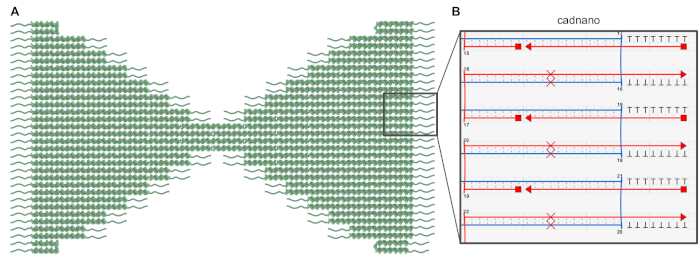
Figure 1: Design of the bowtie DNA origami. (A) Schematic representation of the bowtie origami design in which the core structure is shown as double helices and the polyT-overhangs are depicted as wavy lines. (B) Screenshot of a part of the bowtie origami design in the caDNAno software. The red crosses denote the base pair skipping for the twist correction, and the T8-overhangs are added to prevent blunt-end base-stacking. Please click here to view a larger version of this figure.
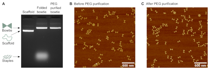
Figure 2: Characterization of the bowtie DNA origami structure. (A) Agarose gel electrophoresis of the bowtie structure before and after poly(ethylene glycol) (PEG) purification. The 7249 nucleotides long scaffold is used as reference. (B) Atomic force microscopy (AFM) image of the bowtie structures before the purification. (C) AFM image of the bowtie structures after PEG purification. Please click here to view a larger version of this figure.
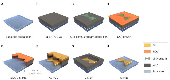
Figure 3: Scheme of fabrication process flow (the dimensions are not in scale). (A) Dice and clean the substrate. (B) Deposit an a-Si layer by plasma-enhanced chemical vapor deposition (PECVD). *It is possible to employ an additional sacrificial layer under the a-Si to enable lift-off with etchant other than HF. (C) Treat the sample surface with O2 plasma and deposit DNA origami onto it. (D) Grow the SiO2 mask in desiccator. (E) Etch a thin layer of SiO2 and through the a-Si underneath it by reactive ion etching (RIE). (F) Deposit metal through the mask by physical vapor deposition (PVD). (G) Lift-off with HF. (H) remove the remaining a-Si by RIE. Please click here to view a larger version of this figure.
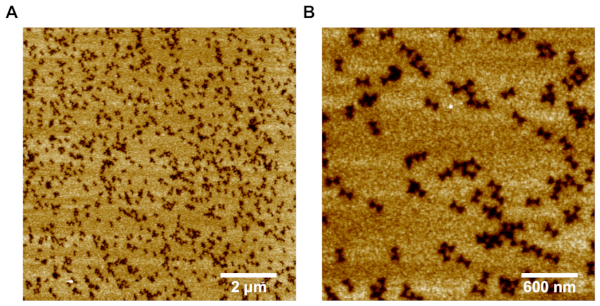
Figure 4: Representative AFM images of SiO2 film with the DNA origami shaped pattern. (A) 10 μm x 10 μm scanning area demonstrates the high yield of the pattern formation. (B) A closer 3 μm x 3 μm scan shows the accurate individual patterns in the SiO2 film. Please click here to view a larger version of this figure.
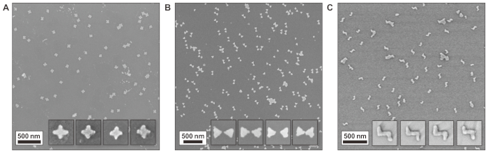
Figure 5: Representative scanning electron microscopy (SEM) images of metallic nanostructures templated with structurally different DNA origami. (A) Cross-shaped DNA origami, i.e., so-called Seeman tile origami54. (B) Bowtie antennas. (C) Chiral double-L (CDL) structures. Insets show individual structures with box sizes of 150 nm x 150 nm. The fabrication yield of exact structures is up to 76% for the bowtie origami and ~ 50% for the other structures displayed here34. This figure has been adapted and modified from Shen et al.34. The figure is reproduced with permission of the authors and published by The American Association for the Advancement of Science, 2018. Please click here to view a larger version of this figure.
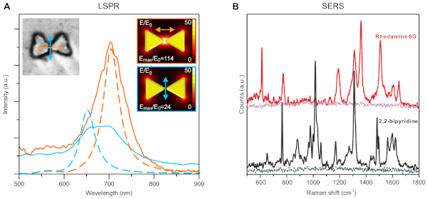
Figure 6: Representative optical/functional properties of resulting nanostructures. (A) Localized surface plasmon resonance (LSPR) measurements of an individual gold bowtie structure with different polarization (color coded as orange and blue). The solid lines are measured spectra and the dashed lines are simulation results. Insets show the SEM image of the measured particle (left) and the model used for simulation (right). (B) Surface enhanced Raman spectroscopy (SERS) of rhodamine 6G and 2,2-bipyridine measured on a surface covered with bowtie nanostructures. The baseline of each sample shows the signal level when the nanostructures were absent. This figure has been adapted and modified from Shen et al.34. The figure is reproduced with permission of the authors and published by The American Association for the Advancement of Science, 2018. Please click here to view a larger version of this figure.
Supplemental File 1: CaDNAno file Please click here to download this file.
Supplemental File 2: m13mp18 sequence Please click here to download this file.
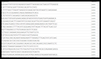
Supplemental File 3: Staple strand sequence Please click here to download this file.
Discussion
The protocol provides great freedom and accuracy in the shape of produced nanostructures. By changing the design of the DNA origami, the shape of the metal nanostructures can be controlled. The final, exact shape of the metal structures is additionally determined by the mask growth step (Step 9) and to a lesser degree by the mask etching (Step 10) should it not be anisotropic. If the mask growth time is extended enough, the holes in the mask will start to grow shut. This can be used to omit the thinnest features of some structures and control gap sizes, as demonstrated in Shen et al.34 with separated triangles of the bowtie origami (Figures 5B). Conversely, thinner shapes can be better preserved by shortening the oxide growth time. This means that it is possible to tune the optical properties displayed in Figure 6, not just by changing the used origami design, but also by tuning the SiO2 film growth.
If the mask thickness is changed significantly, that change must also be reflected in the SiO2 RIE step. Only a very thin layer of SiO2 should be etched (2-5 nm) to barely pierce through the mask holes. This is the most sensitive and crucial part of the whole process. Since the etching time is extremely short, only 10-20 s, exact settings must be experimentally determined when first attempted with new equipment. This is also true for Step 10.4 as some SiO2 is also etched during the a-Si etching. The extent of etched SiO2 is determined by the selectivity of the used a-Si etch parameters, equipment and even individual equipment calibrations. Care should be taken not to etch away the entire SiO2 layer during these two processes.
Another sensitive step is the SiO2 growth. The growth process is dependent on both the chamber humidity and the current activity of the used TEOS. TEOS degrades as it adsorbs water from the air, causing it to become less effective with age. This can manifest as a significantly slower, less controllable growth rate within months even with proper storage of the chemical.34 If the resulting SiO2 layer is thinner than intended, this can indicate a problem with TEOS rather than chamber humidity. While a lower humidity can also result in lower growth rate and thinner film, the resulting film should also be smoother than normal. Meanwhile a coarse grained and rough layer would conversely indicate a problem with high humidity.
It is also possible to perform this protocol on any other freely chosen substrate with two requirements: It must tolerate both HF etching (Step 12) and the 200-300 °C temperatures of PECVD (Step 6). The temperature can be safely lowered to 100 °C for the PECVD of a-Si if a more sensitive substrate is used, but HF cannot be avoided if the protocol is followed exactly as described. To circumvent HF, the application of an additional sacrificial layer would be required. If the requirement of the HF etching is removed, this protocol would become compatible with a wider selection of substrate materials and metals.
As this protocol consists of commonly used and robust micro- and nanofabrication processes, it could be combined with any number of other microfabrication protocols where small feature sizes and complex metal shapes are desired. In the near future, especially with the coming of low-cost DNA origami mass-production31, there is potential for this method to facilitate both general use and high-throughput nanopatterning for interface-based nanophotonics and plasmonics55.
Disclosures
The authors have nothing to disclose.
Acknowledgements
This work was supported by the Academy of Finland (projects 286845, 308578, 303804, 267497), the Jane and Aatos Erkko Foundation, and the Sigrid Jusélius Foundation. This work was carried out under the Academy of Finland Centers of Excellence Programme (2014–2019). We acknowledge the provision of facilities and technical support by Aalto University Bioeconomy Facilities and OtaNano – Nanomicroscopy Center (Aalto-NMC) and Micronova Nanofabrication Center.
Materials
| Name | Company | Catalog Number | Comments |
|---|---|---|---|
| Acetone | Honeywell | 40289H | Semiconductor grade ULSI, ≥ 99.5 % |
| Agarose | Fisher Bioreagents | 1036603 | Low-EEO, multi-purpose and molecular biology grade |
| Ammonium hydroxide | Fisher Chemical | 10652251 | 25 % ammonia solution, Certified AR for Analysis, d = 0.91 |
| BRANSON 5510 | Branson | Ultrasonic bath | |
| Dimension Icon | Bruker | Atomic force microscope | |
| Electron-beam evaporator IM-9912 | Instrumentti Mattila | Evaporator for PVD | |
| Ethidium bromide | Sigma Aldrich | E8751 | Fluorescent dye for DNA staining |
| Eon Microplate spectrophotometer | BioTek | UV/Vis spectrophotometer used for DNA origami concentration measurements | |
| Gel Doc XR+ Documentation System | BioRad | Gel imaging system | |
| Gel Loading Dye, Blue (6×) | New England Biolabs | B7021S | Bromophenol blue-based loading dye for agarose gel electrophoresis |
| G-storm GS1 Thermal cycler | Gene Technologies | ||
| HBR 4 | IKA | Heating bath | |
| Hydrofluoric acid | Honeywell | 40213H | Semiconductor grade, 49.5-50.5 % |
| Isopropanol | Honeywell | 40301H | Semiconductor grade VLSI, ≥ 99.8 % |
| Magnesium chloride | Sigma Aldrich | M8266 | Anhydrous, ≥ 98 % |
| Mini-Sub Cell GT Horizontal Electrophoresis System | BioRad | ||
| Plasmalab 80+ PECVD | Oxford Instruments | PECVD system | |
| Plasmalab 80+ RIE | Oxford Instruments | RIE system | |
| Poly(ethylene glycol) | Sigma Aldrich | 89510 | BioUltra, 8,000 |
| PowerPac HC High-Current Power Supply | BioRad | ||
| Sapphire substrate (Al2O3) | University Wafer | Thickness: 430 μm, Polish: DSP, Size: 50.8 mm | |
| Sigma VP | Zeiss | Scanning electron microscope | |
| Silica gel | Merck | 1019691000 | With indicator (orange gel), granulate ~1-3 mm |
| Single-stranded Scaffold DNA, type p7249 | Tilibit Nanosystems | At 100 nM concentration | |
| Sodium chloride | Sigma Aldrich | S9888 | ACS reagent, ≥ 99.0 % |
| Staple strands (oligonucleotides) | Integrated DNA Technologies | Sequences can be ordered e.g. at 100 micromolar in Rnase-free water | |
| TAE buffer (50×) pH 8.0 | VWR Chemicals | 444125D | Electran Electrophoresis grade |
| Take3 micro-volume plate | BioTek | Used for DNA origami concentration measurements | |
| Tetraethyl orthosilicate | Sigma Aldrich | 86578 | ≥ 99.0 % (GC) |
References
- Seeman, N. C., Sleiman, H. F. DNA nanotechnology. Nature Reviews Materials. 3 (1), 17068(2017).
- Linko, V., Dietz, H. The enabled state of DNA nanotechnology. Current Opinion in Biotechnology. 24 (4), 555-561 (2013).
- Rothemund, P. W. K. Folding DNA to create nanoscale shapes and patterns. Nature. 440 (7082), 297-302 (2006).
- Hong, F., Zhang, F., Liu, Y., Yan, H. DNA Origami: Scaffolds for Creating Higher Order Structures. Chemical Reviews. 117 (20), 12584-12640 (2017).
- Maune, H. T., et al. Self-assembly of carbon nanotubes into two-dimensional geometries using DNA origami templates. Nature Nanotechnology. 5 (1), 61-66 (2010).
- Hung, A. M., et al. Large-area spatially ordered arrays of gold nanoparticles directed by lithographically confined DNA origami. Nature Nanotechnology. 5 (2), 121-126 (2010).
- Kuzyk, A., et al. DNA-based self-assembly of chiral plasmonic nanostructures with tailored optical response. Nature. 483 (7389), 311-314 (2012).
- Zhang, T., et al. 3D DNA Origami Crystals. Advanced Materials. 30 (28), 1800273(2018).
- Julin, S., et al. DNA origami directed 3D nanoparticle superlattice via electrostatic assembly. Nanoscale. 11 (10), 4546-4551 (2019).
- Fu, J., Liu, M., Liu, Y., Yan, H. Spatially-Interactive Biomolecular Networks Organized by Nucleic Acid Nanostructures. Accounts of Chemical Research. 45 (8), 1215-1226 (2012).
- Linko, V., et al. DNA-based enzyme reactors and systems. Nanomaterials. 6 (8), 139(2015).
- Ramakrishnan, S., Subramaniam, S., Stewart, A. F., Grundmeier, G., Keller, A. Regular Nanoscale Protein Patterns via Directed Adsorption through Self-Assembled DNA Origami Masks. ACS Applied Materials & Interfaces. 8 (45), 31239-31247 (2016).
- Grossi, G., Jaekel, A., Andersen, E. S., Saccà, B. Enzyme-functionalized DNA nanostructures as tools for organizing and controlling enzymatic reactions. MRS Bulletin. 42 (12), 920-924 (2017).
- Douglas, S. M., Bachelet, I., Church, G. M. A logic-gated nanorobot for targeted transport of molecular payloads. Science. 335 (6070), 831-834 (2012).
- Li, S., et al. A DNA nanorobot functions as a cancer therapeutic in response to a molecular trigger in vivo. Nature Biotechnology. 36 (3), 258-264 (2018).
- Zhao, Y. -X., et al. DNA origami delivery system for cancer therapy with tunable release properties. ACS Nano. 6 (10), 8684-8691 (2014).
- Kollmann, F., et al. Superstructure-Dependent Loading of DNA Origami Nanostructures with a Groove-Binding Drug. ACS Omega. 3 (8), 9441-9448 (2018).
- Zhang, D. Y., Seelig, G. Dynamic DNA nanotechnology using strand-displacement reactions. Nature Chemistry. 3 (2), 103-113 (2011).
- Ijäs, H., Nummelin, S., Shen, B., Kostiainen, M. A., Linko, V. Dynamic DNA Origami Devices: from Strand-Displacement Reactions to External-Stimuli Responsive Systems. International Journal of Molecular Sciences. 19 (7), 2114(2018).
- Li, J., Fan, C., Pei, H., Shi, J., Huang, Q. Smart Drug Delivery Nanocarriers with Self-Assembled DNA Nanostructures. Advanced Materials. 25 (32), 4386-4396 (2013).
- Linko, V., Ora, A., Kostiainen, M. A. DNA Nanostructures as Smart Drug-Delivery Vehicles and Molecular Devices. Trends in Biotechnology. 33 (10), 586-594 (2015).
- Jiang, Q., Liu, S., Liu, J., Wang, Z. G., Ding, B. Rationally Designed DNA-Origami Nanomaterials for Drug Delivery In Vivo. Advanced Materials. , (2018).
- Shen, B., Linko, V., Dietz, H., Toppari, J. J. Dielectrophoretic trapping of multilayer DNA origami nanostructures and DNA origami-induced local destruction of silicon dioxide. Electrophoresis. 36 (2), 255-262 (2015).
- Kuzyk, A., Jungmann, R., Acuna, G. P., Liu, N. DNA Origami Route for Nanophotonics. ACS Photonics. 5 (4), 1151-1163 (2018).
- Liu, N., Liedl, T. DNA-Assembled Advanced Plasmonic Architectures. Chemical Reviews. 118 (6), 3032-3053 (2018).
- Bathe, M., Rothemund, M. DNA Nanotechnology: A Foundation for Programmable Nanoscale Materials. MRS Bulletin. 42 (12), 882-888 (2017).
- Pilo-Pais, M., Acuna, G. P., Tinnefeld, P., Liedl, T. Sculpting light by arranging optical components with DNA nanostructures. MRS Bulletin. 42 (12), 936-942 (2017).
- Graugnard, E., Hughes, W. L., Jungmann, R., Kostiainen, M. A., Linko, V. Nanometrology and super-resolution imaging with DNA. MRS Bulletin. 42 (12), 951-959 (2017).
- Zhong, J., et al. Metallized DNA nanolithography for encoding and transferring spatial information for graphene patterning. Nature Communications. 4, 1663(2013).
- Zhang, G., Surwade, S. P., Zhou, F., Liu, H. DNA nanostructure meets nanofabrication. Chemical Society Reviews. 42 (7), 2488-2496 (2013).
- Praetorius, F., Kick, B., Behler, K. L., Honemann, M. N., Weuster-Botz, D., Dietz, H. Biotechnological mass production of DNA origami. Nature. 552 (7683), 84-87 (2017).
- Linko, V., et al. One-step large-scale deposition of salt-free DNA origami nanostructures. Scientific Reports. 5, 15634(2015).
- Arbabi, A., Horie, Y., Bagheri, M., Faraon, A. Dielectric metasurfaces for complete control of phase and polarization with subwavelength spatial resolution and high transmission. Nature Nanotechnology. 10 (11), 937-943 (2015).
- Shen, B., et al. Plasmonic nanostructures through DNA-assisted lithography. Science Advances. 4 (2), (2018).
- Douglas, S. M., et al. Rapid prototyping of 3D DNA-origami shapes with caDNAno. Nucleic Acids Research. 37 (26), 5001-5006 (2009).
- Ke, Y., et al. Multilayer DNA Origami Packed on a Square Lattice. Journal of the American Chemical Society. 131 (43), 15903-15908 (2009).
- Dietz, H., Douglas, S. M., Shih, W. M. Folding DNA into twisted and curved nanoscale shapes. Science. 325 (5941), 725-730 (2009).
- Castro, C. E., et al. A primer to scaffolded DNA origami. Nature Methods. 8 (3), 221-229 (2011).
- Kim, D. -N., Kilchherr, F., Dietz, H., Bathe, M. Quantitative prediction of 3D solution shape and flexibility of nucleic acid nanostructures. Nucleic Acids Research. 40 (7), 2862-2868 (2011).
- Benson, E., et al. DNA rendering of polyhedral meshes at the nanoscale. Nature. 523 (7561), 441-444 (2015).
- Veneziano, R., et al. Designer nanoscale DNA assemblies programmed from the top down. Science. 352 (6923), 1534(2016).
- Linko, V., Kostiainen, M. A. Automated design of DNA origami. Nature Biotechnology. 34 (8), 826-827 (2016).
- Nummelin, S., Kommeri, J., Kostiainen, M. A., Linko, V. Evolution of Structural DNA Nanotechnology. Advanced Materials. 30 (24), 1703721(2018).
- Maffeo, C., Yoo, J., Aksimentiev, A. De novo reconstruction of DNA origami structures through atomistic molecular dynamics simulation. Nucleic Acids Research. 44 (7), 3013-3019 (2016).
- Stahl, E., Martin, T. G., Praetorius, F., Dietz, H. Facile and Scalable Preparation of Pure and Dense DNA Origami Solutions. Angewandte Chemie International Edition. 53 (47), 12735-12740 (2014).
- Shaw, A., Benson, E., Högberg, B. Purification of Functionalized DNA Origami Nanostructures. ACS Nano. 9 (5), 4968-4975 (2015).
- Kuzyk, A., Yurke, B., Toppari, J. J., Linko, V., Törmä, P. Dielectrophoretic Trapping of DNA Origami. Small. 4 (4), 447-450 (2008).
- Lin, C., Perrault, S. D., Kwak, M., Graf, F., Shih, W. M. Purification of DNA-origami nanostructures by rate-zonal centrifugation. Nucleic Acids Research. 41 (2), 40(2013).
- Douglas, S. M., et al. Self-assembly of DNA into nanoscale three-dimensional shapes. Nature. 459 (7245), 414-418 (2009).
- Ramakrishnan, S., Ijäs, H., Linko, V., Keller, A. Structural stability of DNA origami nanostructures under application-specific conditions. Computational and Structural Biotechnology Journal. 16, 342-349 (2018).
- Kielar, C., et al. On the Stability of DNA Origami Nanostructures in Low-Magnesium Buffers. Angewandte Chemie International Edition. 57 (30), 9470-9474 (2018).
- Surwade, S. P., et al. Nanoscale growth and patterning of inorganic oxides using DNA nanostructure templates. Journal of the American Chemical Society. 135 (18), 6778-6781 (2013).
- Shen, B., Linko, V., Tapio, K., Kostiainen, M. A., Toppari, J. J. Custom-shaped metal nanostructures based on DNA origami silhouettes. Nanoscale. 7 (26), 11267-11272 (2015).
- Liu, W., Zhong, H., Wang, R., Seeman, N. C. Crystalline Two-Dimensional DNA-Origami Arrays. Angewandte Chemie International Edition. 50 (1), 264-267 (2011).
- Shen, B., Kostiainen, M. A., Linko, V. DNA Origami Nanophotonics and Plasmonics at Interfaces. Langmuir. 34 (49), 14911-14920 (2018).
Reprints and Permissions
