We describe a flash infrared annealing method used for the synthesis of perovskite and mesoscopic-TiO2 films. Annealing parameters are varied and optimized for processing on fluorine-doped tin oxide (FTO) glass and indium tin oxide-coated polyethylene terephthalate (ITO PET), subsequently giving devices power conversion efficiencies >20%.
Method Article
Flash Infrared Annealing for Perovskite Solar Cell Processing
In This Article
Summary
Abstract
Organic–inorganic perovskites have an impressive potential for the design of next generation solar cells and are currently considered for upscaling and commercialization. Currently, perovskite solar cells rely on spin-coating which is neither practical for large areas nor environmentally friendly. Indeed, one of the conventional and most effective lab-scale methods to induce perovskite crystallization, the antisolvent method, requires an amount of toxic solvent that is difficult to apply on larger surfaces. To solve this problem, an antisolvent-free and rapid thermal annealing process called flash infrared annealing (FIRA) can be used to produce highly crystalline perovskite films. The FIRA oven is composed of an array of near-infrared halogen lamps with an illumination power of 3,000 kW/m2. A hollow aluminum body enables an effective water-cooling system. The FIRA method allows the synthesis of perovskite films in less than 2 s, achieving efficiencies >20%. FIRA has a unique potential for the industry because it can be adapted to continuous processing, is antisolvent-free, and does not require lengthy, hour-long annealing steps.
Introduction
Since their inception in 2009, solar cells based on lead halide perovskites have demonstrated unprecedented growth, with power conversion efficiencies (PCE) increasing from 3.8%1 to 25.2%2 in just over a decade of development. Recently, there has also been interest in the development of perovskite solar cells (PSCs) on flexible substrates such as polyethylene terephthalate (PET) as they are lightweight, cheap, applicable to roll-to-roll manufacturing and can be used to power flexible electronics3,4. In the past decade, the PCE of flexible PSCs has improved significantly from 2.62% to 19.1%5.
The majority of the current processing methods for PSCs involve deposition of the perovskite precursor solution, addition of an antisolvent (AS) such as chlorobenzene to induce nucleation and finally thermal annealing to evaporate the solvent and promote crystallization of the perovskite in the desired morphology6,7,8,9. This method requires moderate amounts of organic solvent (~100 µL per 2 x 2 cm substrate) that is typically not reclaimed, is difficult to apply on large-area substrates and is not always reproducible. Additionally, the perovskite layer requires annealing at >100 °C for up to 120 min while the mesoporous-TiO2 electron transporting layer requires sintering at 450 °C for at least 30 min, which not only leads to a large electronic cost and a potential bottleneck in the eventual upscaling of PSCs, but is also incompatible with flexible substrates which typically cannot sustain heating at ≥250 °C10,11,12. Alternative manufacturing methods must, therefore, be found to commercialize this technology3,13,14.
Flash infrared annealing, first reported in 201511, is a low-cost, environmentally friendly and rapid method for the synthesis of compact and defect-tolerant perovskite and metal oxide thin films that eliminates the need for an antisolvent and is compatible with flexible substrates. In this method, freshly-spin-coated perovskite films are exposed to near-IR radiation (700–2,500 nm, peaking at 1,073 nm). Both TiO2 and perovskite have low absorbance in this region, whereas FTO is a strong NIR absorber and rapidly heats up, evaporating the solvent and indirectly annealing the active material11,15. A short 2 s pulse can heat the FTO substrate to 480 °C, while the perovskite remains at ~70 °C, promoting vertical evaporation of the solvent and lateral growth of crystals across the substrate. Heat is quickly dissipated via cooling from the external case, and within seconds, room temperature is reached.
The nucleation and crystallization processes, and thus the final morphology of the film, can be varied through FIRA parameters such as pulse length, frequency, and intensity, allowing for a much more reproducible and controllable crystal growth16. Assuming time-limited nucleation, the pulse length determines the nucleation density whereas the pulse intensity determines the energy provided for crystallization. Insufficient energy would result in incomplete solvent evaporation or crystallization, whereas excess energy would result in thermal degradation of the perovskite15. Optimization of these factors is, therefore, important for the formation of a homogeneous perovskite film, which can affect the optoelectronic properties of the final device.
Compared to the AS method, FIRA has a slower nucleation and faster crystal growth, leading to larger crystalline domains (~40 µm for FIRA vs ~200 nm for AS)16. The lower nucleation rate could be due to a lower supersaturation or a limited nucleation phase as controlled by the duration of the pulse15. However, the difference in grain size does not affect charge carrier mobility and lifetime (mobility ~15 cm2/Vs for AS and ~19 cm2/Vs for FIRA)17 and gives films with similar structural and optical properties, as measured by X-ray diffraction (XRD) and photoluminescence (PL)12. In fact, reports suggest that larger grain sizes are favorable due to suppressed perovskite degradation at grain boundaries4. Compact, defect-tolerant, and highly crystalline perovskite films can be formed with both methods, giving devices with >20% PCE18.
Additionally, the elimination of the antisolvent and the reduction in annealing time from hours to seconds make it much more cost-effective and environmentally friendly. With this method, a crystalline mesoscopic-TiO2 layer can also be manufactured, reducing the energy-intensive sintering step (at 450 °C for 30 min, 1–3 h in total) to just 10 min16,18. TiO2 annealing times as short as seconds have also been previously reported using variations of this method19,20,21,22. As a result, a whole PSC can be fabricated in less than an hour18. This method is also compatible with industrial upscaling and commercialization as it can be adapted to large-area deposition and roll-to-roll processing for fast and synchronized throughput production15. Furthermore, the water-cooling system allows rapid heat dissipation, making it suitable for the fabrication of devices on flexible substrates such as PET.
FIRA can be used for any wet, thin film that can be deposited via a simple solution process and crystallized at different temperatures up to 1,000 °C. The parameters can be optimized such that crystals in the desired morphology are formed. For example, it has been used for the synthesis of various perovskite compositions on glass and PET12,15,18, as well as the mesoscopic-TiO2 layer on glass, giving devices of >20% PCE18. It also allows for the study of phase evolution against temperature, as the oven and substrate surface temperatures are measured to give a temperature profile of the crystallization process16,17.
This paper firstly discusses the protocol used for the optimization of annealing parameters to synthesize a compact, defect-tolerant, and homogeneous perovskite (MAPbI3) film, which simultaneously offers insight into perovskite morphology evolution against temperature/pulse time. Secondly, a protocol for the processing of perovskite solar cells with FIRA-annealed mesoscopic-TiO2 and perovskite layers is discussed. For this study, a perovskite composition based on formamidinium (80%), caesium (15%), and guanidinium (5%) cations was used (herein denoted FCG), and a tetrabutyl ammonium iodide (TBAI) post-treatment was carried out. Therefore, this paper aims to demonstrate the versatility of the FIRA method, its advantages over the conventional antisolvent method, and its potential to be applied in the eventual commercialization of perovskite solar cells20,21,22.
This protocol is divided into 4 sections: 1) A general description of the operation of the FIRA oven 2) Process for the optimization and synthesis of a MAPbI3 perovskite film on FTO glass 3) Processing of FCG perovskite solar cells and 4) Synthesis of MAPbI3 films on ITO-PET.
Protocol
1. Operation of the FIRA Oven
NOTE: A schematic of the FIRA oven, developed in-house, is shown in Figure 1A. The FIRA oven is composed of an array of six near-infrared halogen lamps (peak emission at wavelength of 1,073 nm) with an illumination power of 3,000 kW/m2 and a total output power of 9,600 kW. A hollow aluminum body provides an effective water-cooling system and it in turn allows rapid thermal energy dissipation (within seconds). It is kept in a nitrogen glovebox, and N2 is continuously flowed through the chamber via a gas inlet to keep it under an inert atmosphere, except during annealing. O2 can also be introduced when annealing metal oxide films to promote oxidation.
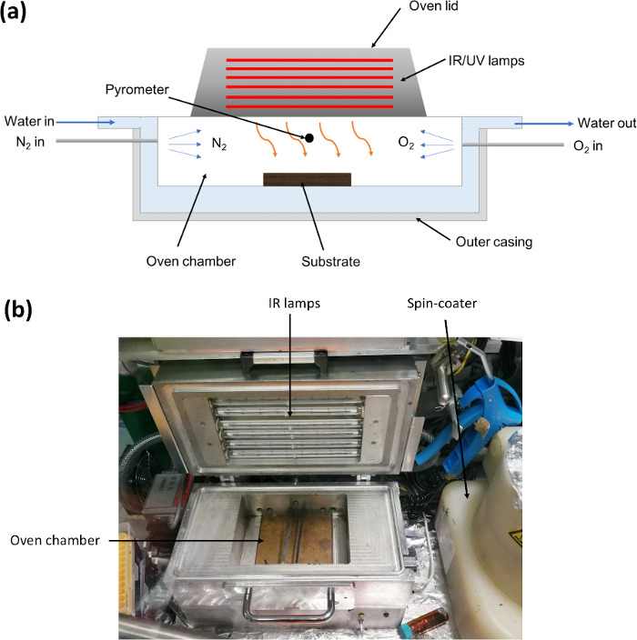
Figure 1: (A) Schematic showing cross-section of the FIRA oven. The oven chamber is continuously cooled by water flowing through the case and kept under an N2 atmosphere. (B) Picture of the FIRA oven. Please click here to view a larger version of this figure.
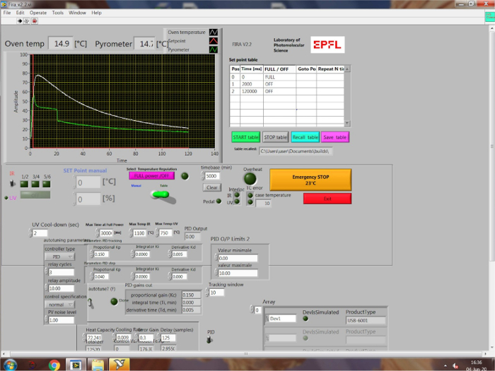
Figure 2: Interface of the FIRA software. The panel on the left shows the temperature profile, which displays the set point (input program), oven temperature, and pyrometer (substrate surface) temperature. The desired annealing program is inputted on the table on the right. Please click here to view a larger version of this figure.
- Programming of annealing cycles
- Connect the FIRA oven to a computer, from which it can be controlled via a guide user interface (Figure 2) on an in-house software. Based on the experiment, select full-power mode or PID (proportional-integral-derivative) mode. In full-power mode, the IR lamps are either completely on or off, whereas in PID mode, the oven is held at a specific temperature for a certain amount of time by intensity modulation.
- Ensure Table is selected on the Table/Manual toggle and input a timebase that is longer than the total duration of the annealing and cooling processes.
- Full-power mode: Input the times at which the lamps should be on or off in the table on the right of the interface. In this way, single pulses as well as annealing cycles can be programed, allowing control of the pulse length and frequency. This is suitable for films that can be rapidly annealed, or for substrates that cannot tolerate sustained heating (e.g, ~1.5–2 s for perovskite films).
- PID mode: Input the time and temperature at which the oven should be irradiated in the table. Similar to the working principle of a traditional hotplate, the intensity of the heating source can be modulated. This is suitable for films that typically require longer annealing times (e.g., 15 min at 100 °C for TBAI).
- Data acquisition: Download the temperature profile displayed on the left of the interface as a .txt or spreadsheet file by right-clicking on the profile and then click on Export File.
NOTE: The software is used for both data acquisition and system control, where the main raw data acquired is the temperature profile. On the temperature profile (Figure 2), the input program is represented by the “set point”. The oven temperature (measured by a K-type thermocouple) and substrate temperature (estimated by a pyrometer) are displayed in real time, giving insight into the thin film crystallization conditions. Please note that the oven temperature does not scale directly with traditional hot plate temperatures as the thermocouple is also directly exposed to IR radiation. Rather, it serves as a reference point for comparison between different FIRA annealing parameters.
- General annealing process
- Deposit the precursor via a suitable solution process: spin-coating26, dip-coating27, or doctor-blading28.
- Transfer the substrates into the FIRA oven chamber and close the oven lid. Ensure that nitrogen flow into the chamber is turned off by closing the gas inlet valve.
- Start and stop the annealing by clicking on START table and STOP table on the computer. Alternatively, connect the FIRA oven to a foot pedal, which can also be used to start and stop the program. As a result, annealing can be carried out without removing one’s hands from the glovebox, allowing for a much smoother and synchronized process.
- When the oven temperature reaches room temperature, remove the substrates from the oven chamber.
2. MAPbI3 Perovskite Film Synthesis and Optimization on FTO Glass
- Perovskite Solution Preparation
- Dissolve methylammonium iodide in anhydrous DMF:DMSO 2:1 v/v to obtain a 1.9 M solution.
- Add an equimolar amount of PbI2 to the solution and dilute with anhydrous DMF:DMSO 2:1 v/v to give a 1.4 M methylammonium lead iodide precursor solution. Heat at 80 °C until complete dissolution and cool to room temperature.
NOTE: The solution is prepared and stored in an argon glovebox. The protocol can be paused here.
- Perovskite film synthesis
- Use FTO coated glass substrates of 1.7 cm x 2.5 cm.
- Clean the substrates via successive sonication in cleaning soap (2 vol % in deionized H2O), acetone and ethanol for 15 min each, then dry them with compressed air.
- Treat the substrates under UV/ozone in a plasma cleaner for 15 min.
- Input the desired annealing program as per section 1.1.
- Blow the substrate surface with a nitrogen gun to remove dust and other impurities.
- Spin-coat 50 µL of the perovskite precursor at 4,000 rpm for 10 s, with an acceleration of 2000 rpm·s-1.
- Immediately after deposition, transfer the substrate to the FIRA oven for annealing at a range of pulse times as desired (0–7 s used herein, optimized pulse is 2 s). Start the inputted annealing program by pressing START on the software or stepping on the foot pedal. A color change from yellow to black should be observed, indicating the formation of a 3D perovskite structure.
- Remove the substrate when the oven temperature reaches 25 °C.
- Store the annealed films in a dry air box.
NOTE: The FIRA oven and the spin-coater are placed in the same nitrogen glovebox such that solution deposition and annealing can be carried out smoothly and under an inert atmosphere.
- Material characterization
- Capture optical images on a polarizing microscope equipped with a xenon light source and infinitely corrected objectives of 10x and 50x.
- Record absorbance spectra simultaneously with an optical fiber integrated into the microscope set-up and connected to a spectrometer (spectral range 300–1,100 nm).
NOTE: The above characterization can be done immediately after annealing, allowing for rapid screening of film quality. The measurements are taken in ambient air and temperature. More in-depth characterization such as scanning electron microscopy (SEM) and X-ray diffraction can be subsequently carried out (see section 3.7).
3. FCG perovskite solar cell processing
- Substrate preparation and cleaning
- Etch one side of the FTO glass substrates with Zn powder and 4 M HCl.
- Clean substrates via successive sonication in cleaning soap (2 vol % in deionized H2O) for 30 min and isopropanol for 15 min, and dry with compressed air.
- Treat under UV/ozone in a plasma cleaner for 5 min.
- Compact TiO2 layer
- Heat FTO glass substrates to 450 °C on a sintering hot plate and keep them at this temperature for 15 min before solution deposition.
- Dilute 0.6 mL of titanium diisopropoxide bis(acetylacetonate) and 0.4 mL of acetylacetone in 9 mL of EtOH to give the precursor solution.
- Deposit the solution via spray pyrolysis with oxygen as the carrier gas (0.5 bar) at 45° and a distance of ~20 cm. Leave an interval of 20 s between each spraying cycle.
- Leave the substrates at 450 °C for 5 min more, then cool to room temperature. This gives a compact TiO2 layer of ~30 nm.
NOTE: The protocol can be paused here. If the next step is not carried out immediately, re-sinter the substrate at 450 °C for 30 min before deposition of the mesoporous-TiO2 layer.
- Mesoporous-TiO2 layer
- Make a precursor solution by diluting TiO2 paste (particle size 30 nm) in EtOH at a concentration of 75 mg/mL. Stir the solution with a magnetic stirrer bar until complete dissolution.
- Spin-coat 50 µL of the solution at 4,000 rpm for 10 s, with a ramp of 2,000 rpm·s-1.
- Program an annealing cycle of 10 pulses, 15 s on and 45 s off in the table on the software.
- Place the substrates in the FIRA oven, and anneal under full power mode with the above annealing cycle by pressing Start Table or stepping on the foot pedal. This yields a 150–200 nm layer.
- Remove the samples when the oven temperature reaches 25 °C.
NOTE: Ensure that the oven is at room temperature or below before starting annealing. With the above cycle, the oven temperature reaches ~600 °C during annealing.
- Perovskite layer
- Make a solution of formamidinium iodide (1.12 M), PbI2 (1.4 M), CsI (0.21 M) and GAI (0.07 M) in anhydrous DMF:DMSO 2:1 v/v.
- Spin-coat 40 µL of the solution at 4,000 rpm for 10 s.
- Program an annealing step of 1.6 s on full power mode on the software (this reaches ~90 °C).
- Transfer the substrate to the FIRA oven and start annealing by pressing Start Table or stepping on the foot pedal. The surface should turn from yellow to black.
- Leave the samples in the oven for an additional 10 s for cooling before removal.
- Tetrabutyl ammonium iodide (TBAI) post-treatment (optional)
- Dissolve 3 mg of tetrabutyl ammonium iodide in 1 mL of isopropanol.
- Spin-coat the solution at 4,000 rpm for 20 s.
- Program an annealing step at 100 °C for 15 min using PID mode.
- Transfer the substrate to the FIRA oven and anneal with the above program. Cool to 25 °C before the next step.
- Hole transporting material and top electrode
- Dissolve spiro-OMeTAD in chlorobenzene (70 mM) and add 4-tert-butylpyridine (TBP), Lithium bis(trifluoromethylsulphonyl)imide) (Li-TFSI, 1.8 M in acetonitrile) and Tris(2-(1H-pyrazol-1-yl)-4-tert-butylpyridine)-cobalt(III) Tris(bis(trifluoromethylsulfonyl) imide) (FK209, 0.25 M in acetonitrile) such that the molar ratio of the additives with respect to spiro-OMeTAD are 3.3, 0.5, and 0.03 for TBP, Li-TFSI, and FK209 respectively.
- Deposit 50 µL of the solution at 4,000 rpm for 20 s under dynamic spin-coating, adding the solution 3 s after the start of the program.
- Leave it to oxidize overnight in a dry air box.
- Deposit 80 nm of gold via thermal evaporation under vacuum. Use a shadow mask to pattern the electrodes.
- Photovoltaic device testing and material characterization
- Take photovoltaic measurements using a solar simulator equipped with a xenon arc lamp and a digital source meter. Specify the active area of the device with a black, non-reflective metal mask (0.1024 cm2 used herein). Measure the current-voltage curves under reverse and forward bias at a 10 mV/s scan rate under AM 1.5 G irradiation.
- Take X-ray diffraction patterns with a diffractometer in reflection-spin mode, using Cu Kα radiation and a Ni β filter.
- Take scanning electron microscope images at an acceleration voltage of 3 kV.
4. MAPbI3 films on ITO-PET substrate
- Cut ITO-PET and microscope glass slides into pieces of 1.7 cm x 2.5 cm.
- Clean the glass slides and ITO-PET as per steps 2.2.2–2.2.3.
- Attach the ITO substrates onto the glass slides with double-sided tape, ensuring they are as flat as possible.
- Prepare the MAPbI3 precursor as described in section 2.1. Blow the substrate surface with an N2 gun before spin-coating the solution and annealing the film with FIRA, as per steps 2.2.5–2.2.8, with a pulse time of 1.7 s.
- Carry out material characterization as described in sections 2.3 and 3.7.
Results
Optimization and synthesis of MAPbI3 films on FTO glass
To assess perovskite film quality, microscope images, X-ray diffraction, and absorbance spectra were taken. The optimum pulse time should yield a compact, uniform, and pinhole-free film with large crystal grains. Figure 3 shows optical images of MAPbI3 films at pulse times ranging from 0 s to 7 s, while Figure 4 shows the XRD spectra of films annealed at selective pulse times. These pulse times represent the boundaries of the four distinct perovskite phases observed based on the various characterizations carried out. The phase evolution as a function of pulse time and temperature is shown in Figure 5, and a comparison of the top-view SEM images of films formed by both FIRA and antisolvent methods are found in supplementary information S1. XRD patterns for all pulses and corresponding absorbance spectra are found in supplementary information S2 and S3. Pulses from 0 to 1.6 s gave needle-like crystals or small crystalline domains separated by non-crystalline phases, as evidenced by the precursor peaks at 2θ = 6.59, 7.22, and 9.22°29. For 1.8 to 3.8 s pulses, well-defined crystal grains were formed, and XRD patterns showed the formation of the MAPbI3 tetragonal I4/mcm phase. This is also confirmed by the absorption onset of 780 nm. However, longer pulse times led to thermal degradation of the perovskite, with complete degradation for pulses >5 s, as shown by the evolution of the PbI2 peak at 2θ = 12.7°. The optimized pulse was determined to be 2 s, giving crystal grains of ~30 µm. Therefore, FIRA allows for a comprehensive study of the nucleation and crystallization processes based on temperature, as controlled by the pulse time. The parameters can also be varied and optimized for different thin films, showing the versatility of this method.
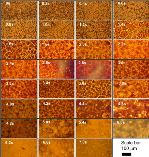
Figure 3: Optical images of MAPbI3 perovskite films on FTO glass, annealed with pulses ranging from 0 s to 7 s. All images were taken at 10x magnification in transmission mode. Please click here to view a larger version of this figure.
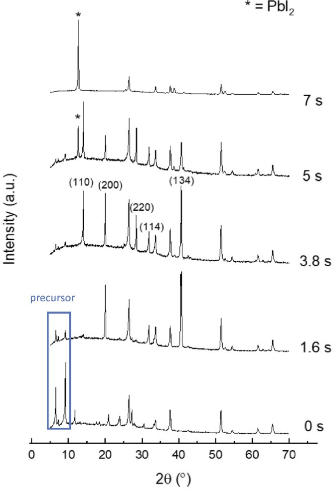
Figure 4: XRD spectra of MAPbI3 films annealed at selective pulse times. Labeled planes are representative of the tetragonal I4/mcm phase. Asterisked peaks represent diffractions from PbI2, while the blue rectangle represents those from the precursor solution. Please click here to view a larger version of this figure.
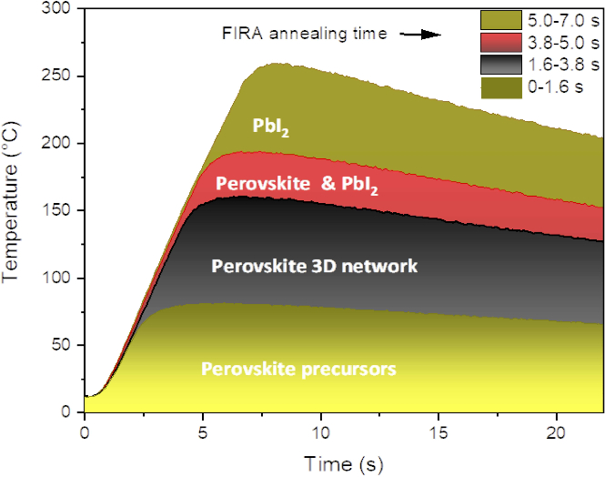
Figure 5: Temperature profile showing perovskite phase evolution as a function of pulse length. The boundary of the different phases has been determined from the corresponding XRD analysis, shown in Figure 4. Adapted from15. Please click here to view a larger version of this figure.
FCG perovskite devices
Figure 6A,B show the temperature profile and XRD pattern of the mesoscopic-TiO2 layer annealed with a FIRA cycle of 10 pulses, 15 s on and 45 s off. With FIRA, temperatures of ~600 °C could be reached and the TiO2 layer can be synthesized in just 10 min, much shorter than the conventional method which requires sintering for 1 h to 3 h, peaking at 450 °C. The resulting film shows no discernible difference to that sintered on a hot plate. As a result, the whole perovskite solar cell could be processed in less than an hour. The cross-sectional SEM image (Figure 6C) shows that the subsequent devices fabricated are very similar to those made via traditional methods, with layers of similar thickness and morphology. Additionally, FIRA-processed devices showed excellent performance (Figure 7), with the champion device showing PCE = 20.1%, FF = 75%, Voc = 1.1 V, and Jsc = 24.4 mA/cm2, comparable to devices fabricated with the antisolvent method. A large-area device with a 1.4 cm2 active area also gave PCE of 17%, showing FIRA is a promising alternative processing method for the manufacture of PSCs.
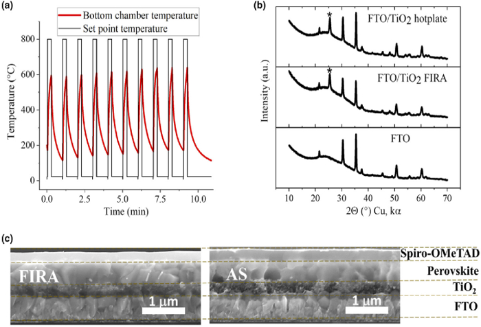
Figure 6: (A) Temperature profile of mesoporous TiO2 annealing in FIRA, with a cycle of 10 pulses of 15 s on and 45 s off. (B) X-ray patterns for TiO2 films annealed with a hotplate and FIRA, and a blank FTO substrate as reference. (C) Cross-sectional SEM images of perovskite solar cell architectures, processed by FIRA and antisolvent. Reproduced with permission from18. Please click here to view a larger version of this figure.
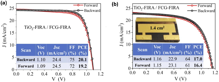
Figure 7: Current-voltage curve for champion FCG perovskite devices. (A) FIRA-annealed mesoporous-TiO2 and perovskite layers. (B) Large area (1.4 cm2) device with FIRA-annealed mesoporous-TiO2 and perovskite layers. Reproduced with permission from18. Please click here to view a larger version of this figure.
MAPbI3 films on ITO-PET
Figure 8 shows optical images of MAPbI3 films annealed at pulses ranging from 1 s to 2 s. At shorter pulse times, there is incomplete crystallization, whereas at pulse times >1.7 s, the PET substrate begins to melt (see Supplemental Figure 4). Thermal degradation of the perovskite is also observed for the 2 s pulse. At the optimized pulse time of 1.7 s, densely packed crystal domains of ~15 µm were observed. Although there are small pinholes of 1–2 µm, it is clear that FIRA can be used to form compact and uniform perovskite films on flexible polymers without melting the substrate, due to rapid cooling from the case, which is a significant advantage compared to hotplate annealing.
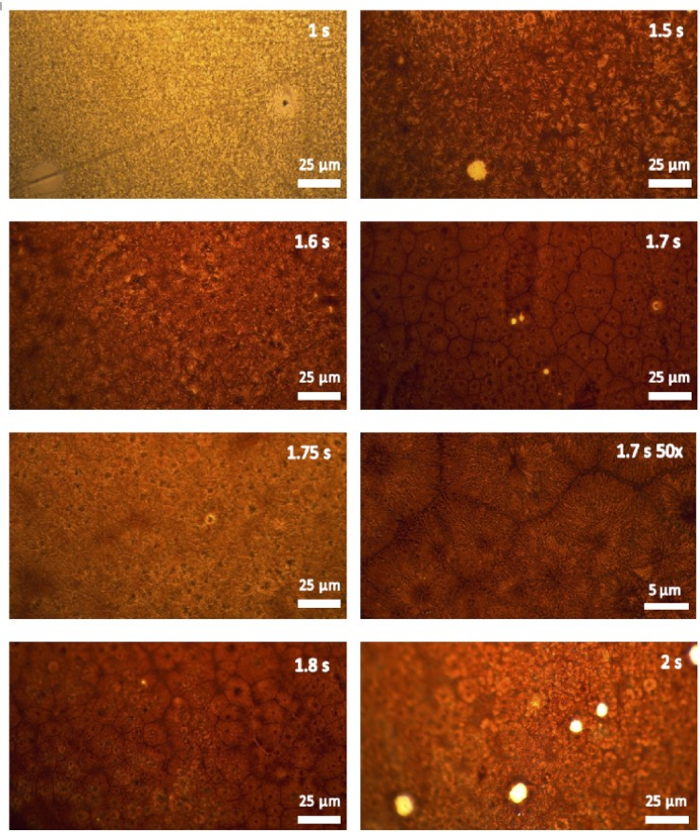
Figure 8: Optical images of MAPbI3 films annealed at various pulse times on ITO-PET. All images are taken in transmission mode and 10x magnification unless otherwise specified. Please click here to view a larger version of this figure.
Supplemental Figure 1: Top-view SEM comparison of FIRA and hotplate annealed perovskite films. (A) Top view of FIRA-annealed perovskite films for four annealing times, scale bar: 25 µm. (B) Top view of a reference film made by the antisolvent method followed by annealing at 100 °C for 1 h on a standard hotplate, scale bar: 1 µm. Adapted from1. Please click here to download this figure.
Supplemental Figure 2: XRD spectra of MAPbI3 films on FTO glass, annealed with pulses of (A) 0–1.4 s (B) 1.6–3 s (C) 3.2–4.6 s (D) 4.8–7 s. Please click here to download this figure.
Supplemental Figure 3: Absorbance spectra of MAPbI3 films on FTO glass, annealed with pulses of (A) 0.2–1.8 s (B) 2–3.6 s (C) 3.8–7 s. Please click here to download this figure.
Supplemental Figure 4: Physical appearance of MAPbI3 films annealed on PET at various pulse lengths. Please click here to download this figure.
Supplemental Figure 5: Temperature profile and top-view SEM images of the pristine paper substrate, ITO electrode, and mesoporous-TiO2 layer processed with FIRA. Please click here to download this figure.
Supplemental Figure 6: Cross-sectional SEM image of perovskite deposited (via antisolvent method) on a FIRA-annealed ITO/TiO2 stack on a paper substrate. ITO np = ITO nanoparticles, pvk = perovskite. Please click here to download this figure.
Discussion
Figure 9 shows the general process of perovskite film annealing with FIRA.
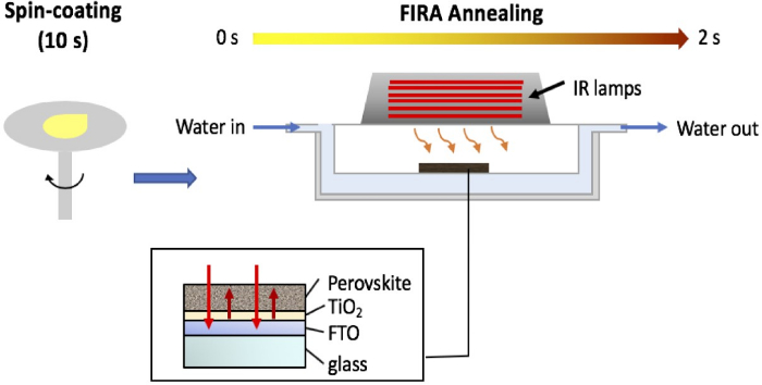
Figure 9: Schematic representation of perovskite film processing with FIRA. The wet film is deposited from the solution by spin-coating and subsequently transferred to the FIRA oven for annealing in ~2 s, giving the black perovskite stable phase. Please click here to view a larger version of this figure.
In the solidification process of a thin film from the solution, the desired final shape will depend on the application: films in energy devices for photocatalysis, battery electrodes, and solar cells can have different morphologies30,31,32,33. Therefore, identifying the optimal parameters for each substrate and wet film interface is a critical step in the protocol to follow. Typically, for PSCs we expect to have shiny and smooth films in order to minimize defects and to enhance the photophysical properties such as charge transport of carriers to give null non-radiative recombination34,35,36. For thin film processing, the main parameters are pulse time, the number of pulses, and the irradiation temperature, which are a balance between forming the desired morphology while being as rapid and energy efficient as possible. Insufficient energy would lead to incomplete solvent evaporation or crystallization, while excess energy would lead to degradation of the material. Therefore, it is crucial to systematically vary the annealing parameters and analyze the resulting film quality (as detailed in sections 2.2, 2.3, and 3.7) to find the optimal parameters for each thin film/substrate combination. Once this is completed, thin films can be synthesized rapidly and reliably. The method relies on its accuracy, for example, the minimum pulse time is 20 ms, allowing one to finely control the temperature ratio for crystal growth. Besides, one can have a wide window for optimization, aided by the data collection of images and absorption spectra for optical and morphological screening.
The FIRA method is still in development, and, as its name implies, it is currently based on IR irradiation. However, the latest version of FIRA includes UV-A radiation generated from a separate metal-halide lamp source. UV and IR can be used for combined wavelength photonic annealing and curing, providing additional functionality. For example, semiconductor curing with FIRA is a straightforward way to improve the wettability of substrates. Additionally, for a multi-layered approach in crystal growth, this selective wavelength annealing can be adapted depending on the material, and the pulse can be modulated depending on the desired shape16,32,37. Current investigations include annealing of an ITO electrode and a mesoscopic-TiO2 layer on paper (the latter using mixed IR/UV annealing, see Supplemental Figure 5 in the supplementary information). As shown in Supplemental Figure 6, a perovskite film can be successfully deposited on the FIRA-annealed ITO/TiO2 stack. This can be applied to a wide range of substrates and thin films in the future.
So far, the FIRA method is limited to the annealing of wet films that can be deposited via solution processes. It depends on the capability of the deposition method, and this is governed by solvent engineering and multi-layered growth based on solutions with approaching solvent polarities. Optimization is also required for each thin film as this is a novel method without a lot of previously reported protocols in literature, which may be time-consuming. Additionally, although FIRA can be used for flexible substrates such as PET and paper as there is rapid cooling from the case, a good contact between the substrate and the oven chamber must be ensured to avoid substrate melting. This may be difficult since flexible substrates are easily bent during processing, but this may be improved by attaching the substrates on a thin glass slide to ensure that they are completely flat and to allow ease of manipulation. However, it is important to note that the absorption of the film will change as the material transitions from non-absorbing (wet NIR-transparent perovskite precursor material) to dry (NIR-absorbing black perovskite) and this additional absorption can contribute to the damage of the substrate38.
Despite these limitations, FIRA still presents many advantages in comparison to the antisolvent method. Firstly, thin films can be synthesized much quicker. For example, the perovskite is formed in <2 s while the mesoporous-TiO2 layer is formed in only 10 min, much shorter than the hours required in the conventional method. The elimination of the antisolvent and the shorter annealing times also mean that there is a much lower energetic and financial cost. Life cycle assessment (Figure 10) of the perovskite synthesis process shows that FIRA presents only 8% of the environmental impact and 2% of the fabrication cost of the antisolvent method. Additionally, it is compatible with flexible and large-area substrates. A total area of 10 x 10 cm2 can be irradiated at one time, and it has already been shown that devices of 1.4 cm2 active area as well as films of 100 cm2 can be synthesized this way. Finally, it is highly reproducible, versatile, and adaptable to fast throughput roll-to-roll manufacturing, as the deposition and annealing steps are carried out continuously in one place in a synchronized and smooth process.
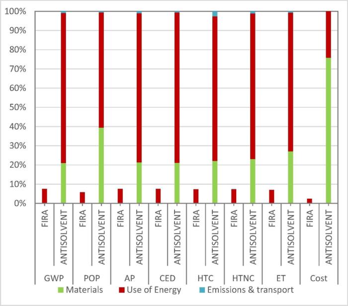
Figure 10: A comparison of the relative cost and environmental impact of FIRA and anti-solvent methods determined by life cycle assessment. GWP = Climate change [kg CO2 eq], POP = Photochemical oxidation [kg C2H4 eq], AP = Acidification [kg SO2 eq], CED = Cumulative energy demand [MJ], HTC = Human Toxicity, cancer effects [CTUh], HTNC = Human Toxicity, non-cancer effects [CTUh], ET = Freshwater ecotoxicity [CTUe]. Reproduced with permission from12. Please click here to view a larger version of this figure.
Current investigations on FIRA are focused on optimization for thin film synthesis on flexible substrates such as paper and PET, as well as for the synthesis of other key component layers of PSCs such as the SnO2 compact layer, or carbon and ITO electrodes. Furthermore, the next step is to fabricate high-performing devices of >5 cm2. Therefore, it can be said that FIRA represents a step toward an environmentally friendly and cost-efficient way to manufacture large-area, commercial PSCs.
Disclosures
The authors have nothing to disclose.
Acknowledgements
The project (WASP) leading to this publication, has received funding from the European Union’s Horizon 2020 Research and Innovation Program under grant agreement No. 825213.
Materials
| Name | Company | Catalog Number | Comments |
|---|---|---|---|
| 4-tert-butylpyridine | Sigma Aldrich | 142379 | |
| Acetonitrile, anhydrous | ACROS Organics | AC610220010 | |
| Acetylacetone | Sigma Aldrich | P7754 | |
| Caesium iodide | Sigma Aldrich | 203033 | |
| Chlorobenzene, anhydrous | ACROS Organics | AC396971000 | |
| Digital source meter | Metrohm | PGSTAT302N Autolab | |
| DMF, anhydrous | ACROS Organics | AC326871000 | |
| DMSO, anhydrous | ACROS Organics | AC326881000 | |
| Ethanol | Sigma Aldrich | 459844 | |
| FIRA Software | Labview | Developed in-house | |
| FK209 | Dyenamo | DN-P04 | |
| Formamidinium iodide | GreatCell Solar | SKU MS150000 | |
| FTO glass | Nippon Sheet Glass | NSG 10 | Sheet resistance = 11-13 ohms/sq |
| Guanidinium iodide | Sigma Aldrich | 806056 | |
| Cleaning Soap | Hellmanex III | - | |
| Hydrochloric acid | Sigma Aldrich | 320331 | |
| Isopropanol | Sigma Aldrich | 190764 | |
| ITO PET | Sigma Aldrich | 639303 | Sheet resistance = 60 ohms/sq |
| Lead iodide | TCI | L0279 | |
| Li-TFSI | Sigma Aldrich | 544094 | |
| Mesoporous TiO2 paste, 3 nrd | GreatCell Solar | SKU MS002300 | |
| Methylammonium iodide | GreatCell Solar | SKU MS1010000 | |
| Microscope | Zeiss | Axio-Scope A1 Polarizing Microscope | |
| Microscope lens | Zeiss | EC Epiplan-Apochromat | |
| Microscope xenon light source | Ocean Optics | HPX-2000 | |
| Optical fibre | Ocean Optics | QP230-2-XSR | 230 μm core |
| Plasma cleaner | Jetlight Company Inc. | UVO-Cleaner Model no. 256-220 | |
| Polymer-planarised paper | Arjowiggins | Powercoat HD | |
| Scanning electron microscope | Zeiss | Merlin Microscope | |
| Sintering hot plate | Harry Gestigkeit GMBH | - | |
| Solar simulator | ABET Technologies | Model 11016 Sun 2000 | |
| Spectrometer | Ocean Optics | Maya2000 Pro | Spectral range: 300-1100 nm |
| Spiro-OMeTAD | Sigma Aldrich | 792071 | |
| Tetrabutyl ammonium iodide | GreatCell Solar | SKU MS106000 | |
| Thermal evaporator | Kurt J. Lesker | - | |
| titanium diisopropoxide bis(acetylacetonate) | Sigma Aldrich | 325252 | |
| X-ray diffractometer | PANanalytical | Empyrean diffractometer (theta-theta, 240 mm) | equipped with a PIXcel-1D detector, Bragg-Brentano beam optics and parallel beam optics |
| Zinc powder | Sigma Aldrich | 324930 |
References
- Kojima, A., Teshima, K., Shirai, Y., Miyasaka, T. Organometal halide perovskites as visible-light sensitizers for photovoltaic cells. Journal of the American Chemical Society. 131 (17), 6050-6051 (2009).
- National Renewable Energy Laboratory. Best Research-Cell Efficiency Chart. National Renewable Energy Laboratory. , Available from: https://www.nrel.gov/pv/assets/pdfs/best-research-cell-efficiencies.20200406.pdf (2020).
- Mujahid, M., Chen, C., Hu, W., Wang, Z. K., Duan, Y. Progress of high-throughput and low-cost flexible perovskite solar cells. Solar RRL. 4, 1900556(2020).
- Feng, J., et al. Record efficiency stable flexible perovskite solar cell using effective additive assistant strategy. Advanced Materials. 30 (35), 1-9 (2018).
- Cao, B., et al. Flexible quintuple cation perovskite solar cells with high efficiency. Journal of Materials Chemistry A. 7 (9), 4960-4970 (2019).
- Green, M. A., Ho-Baillie, A., Snaith, H. J. The emergence of perovskite solar cells. Nature Photonics. 8 (7), 506-514 (2014).
- Park, N. G. Perovskite solar cells: an emerging photovoltaic technology. Materials Today. 18 (2), 65-72 (2015).
- Zhou, H., et al. Interface engineering of highly efficient perovskite solar cells. Science. 345 (6196), 542-546 (2014).
- Jeon, N. J., et al. Compositional engineering of perovskite materials for high-performance solar cells. Nature. 517 (7535), 476-480 (2015).
- Troughton, J., et al. Photonic flash-annealing of lead halide perovskite solar cells in 1 Ms. Journal of Materials Chemistry A. 4 (9), 3471-3476 (2016).
- Troughton, J., et al. Rapid processing of perovskite solar cells in under 2.5 seconds. Journal of Materials Chemistry A. 3 (17), 9123-9127 (2015).
- Sánchez, S., et al. Flash infrared annealing as a cost-effective and low environmental impact processing method for planar perovskite solar cells. Materials Today. 31, 39-46 (2019).
- Park, N. G., Grätzel, M., Miyasaka, T., Zhu, K., Emery, K. Towards stable and commercially available perovskite solar cells. Nature Energy. 1 (11), 16152(2016).
- Song, Z., et al. A technoeconomic analysis of perovskite solar module manufacturing with low-cost materials and techniques. Energy & Environmental Science. 10 (6), 1297-1305 (2017).
- Sanchez, S., Hua, X., Phung, N., Steiner, U., Abate, A. Flash infrared annealing for antisolvent-free highly efficient perovskite solar cells. Advanced Energy Materials. 8, 1702915(2018).
- Sánchez, S., et al. Flash infrared pulse time control of perovskite crystal nucleation and growth from solution. Crystal Growth & Design. 20 (2), 670-679 (2020).
- Muscarella, L. A., et al. Crystal orientation and grain size: do they determine optoelectronic properties of MAPbI3 perovskite. The Journal of Physical Chemistry Letters. 10 (20), 6010-6018 (2019).
- Sánchez, S., Jerónimo-Rendon, J., Saliba, M., Hagfeldt, A. Highly efficient and rapid manufactured perovskite solar cells via flash infraRed annealing. Materials Today. , (2020).
- Watson, T., Mabbett, I., Wang, H., Peter, L., Worsley, D. Ultrafast near infrared sintering of TiO2 layers on metal substrates for dye-sensitized solar cells. Progress in Photovoltaics: Research and Applications. 19 (4), 482-486 (2011).
- Hooper, K., Carnie, M. J., Charbonneau, C., Watson, T. Near infrared radiation as a rapid heating technique for TiO2 films on glass mounted dye-sensitized solar cells. International Journal of Photoenergy. , 953623(2014).
- Carnie, M. J., et al. Ultra-fast sintered TiO2 films in dye-sensitized solar cells: phase variation, electron transport and recombination. Journal of Materials Chemistry A. 1 (6), 2225-2230 (2013).
- Baker, J., et al. High throughput fabrication of mesoporous carbon perovskite solar cells. Journal of Materials Chemistry A. 5 (35), 18643-18650 (2017).
- Berhe, T. A., et al. Organometal halide perovskite solar cells: degradation and stability. Energy & Environmental Sciences. 9 (2), 323-356 (2016).
- Jung, H. S., Park, N. G. Perovskite solar cells: from materials to devices. Small. 11 (1), 10-25 (2015).
- Burschka, J., et al. Sequential Deposition as a route to high-performance perovskite-sensitized solar cells. Nature. 499 (7458), 316-319 (2013).
- Xiao, M., et al. A fast deposition-crystallization procedure for highly efficient lead Iodide perovskite thin-film solar cells. Angewandte Chemie International Edition. 53 (37), 9898-9903 (2014).
- Adnan, M., Lee, J. K. All sequential dip-coating processed perovskite layers from an aqueous lead precursor for high efficiency perovskite solar cells. Scientific Reports. 8 (1), 2168(2018).
- Santa-Nokki, H., Kallioinen, J., Kololuoma, T., Tuboltsev, V., Korppi-Tommola, J. Dynamic preparation of TiO2 films for fabrication of dye-sensitized solar cells. Journal of Photochemistry and Photobiology A: Chemistry. 182 (2), 187-191 (2006).
- Sanchez, S., Steiner, U., Hua, X. Phase evolution during perovskite formation-insight from pair distribution function analysis. Chemistry of Materials. 31 (9), 3498-3506 (2019).
- Virkar, A. A., Mannsfeld, S., Bao, Z., Stingelin, N. Organic semiconductor growth and morphology considerations for organic thin-film transistors. Advanced Materials. 22 (34), 3857-3875 (2010).
- Hoppe, H., Sariciftci, N. S. Morphology of polymer/fullerene bulk heterojunction solar cells. Journal of Materials Chemistry. 16 (1), 45-61 (2006).
- Paquin, F., Rivnay, J., Salleo, A., Stingelin, N., Silva, C. Multi-phase semicrystalline microstructures drive exciton dissociation in neat plastic semiconductors. Journal of Materials Chemistry C. 3 (41), 10715-10722 (2015).
- Diao, Y., Shaw, L., Bao, Z., Mannsfeld, S. C. B. Morphology control strategies for solution-processed organic semiconductor thin films. Energy & Environmental Sciences. 7 (7), 2145-2159 (2014).
- Slotcavage, D. J., Karunadasa, H. I., McGehee, M. D. Light-induced phase segregation in halide-perovskite absorbers. ACS Energy Letters. 1 (6), 1199-1205 (2016).
- Jiang, Q., et al. Surface passivation of perovskite film for efficient solar cells. Nature Photonics. 13 (7), 460-466 (2019).
- Yang, W. S., et al. Iodide Management in formamidinium-lead-halide-based perovskite layers for efficient solar cells. Science. 356 (6345), 1376-1379 (2017).
- Almadhoun, M. N., Khan, M. A., Rajab, K., Park, J. H., Buriak, J. M., Alshareef, H. N. UV-Induced ferroelectric phase transformation in PVDF thin films. Advanced Electronic Materials. 5 (1), 1800363(2019).
- Hooper, K., Smith, B., Baker, J., Greenwood, P., Watson, T. Spray PEDOT:PSS coated perovskite with a transparent conducting electrode for low cost scalable photovoltaic devices. Materials Research Innovations. 19 (7), 482-487 (2015).
Reprints and Permissions
Request permission to reuse the text or figures of this JoVE article
Request Permission