Here, we describe a workflow using laser scanning microscopy to determine the volume electromigrated through a metal line under test. By varying different experimental variables, a multitude of information about electromigration can be acquired. In this work, the length of the onset of electromigration is determined.
Method Article
Using Laser Scanning Microscopy to Determine Electromigration in Molybdenum Disilicide
In This Article
Summary
Abstract
With increasing the current density and decreasing the size of chips electromigration becomes more and more important. Electromigration is the movement of atoms in an electrically conductive material caused by current flowing. For aluminum and copper the electromigration parameters and their dependencies have been investigated by a multitude of people and methods. For other materials, this is not the case. Electromigration experiments often use very long times to stress the lines under test in the median to failure experiments. These experiments only give surface-level information about electromigration. More sophisticated methods look at the microscopic or nanoscale effects and influences. Usually, expensive equipment such as scanning electron microscopes (SEM), synchrotrons, or X-ray microtomography are used for these investigations. A workflow enabling the investigation of electromigration on the microscopic scale by using a laser scanning microscope has been developed. With this laser scanning technique, it is possible to achieve results with slightly less accuracy than SEM but with much less effort in preparing the samples.
With the electromigrated volume being known, the same procedures as with the electromigrated volumes determined via SEM can be used to calculate electromigration parameters. By varying different experimental variables, a multitude of information about electromigration can be achieved. In this work determining the length for the onset of electromigration is shown.
Introduction
Electromigration is the migration of metal ions caused by current. During electromigration, a force  acts on the metal ion.
The force on an ion inside a conductive line under test without an encapsulating layer can be calculated as:

With Z* being the effective ion charge for the ion moving, being the charge of an electron, and  being the electrical field1. For a metal conductor
  with the specific resistivity ρ and the current density
  .
.
Z* depends on the ion species and the material of the line under test. Its value indicates the strength of the electromigration, and its sign indicates the direction of the movement of the ion in question.
This force causes the atoms to move and to be transported in the metal line. Using the relation between the ion velocity  and the driving force
  and the Nernst-Einstein relation for the mobility of the ions
  the atomic flux (number of atoms per unit time per unit area transported by electromigration)
  can be calculated as:
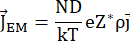
With N being the density of the lattice atoms, the coefficient of diffusion D, k being the Boltzmann constant, and T the absolute temperature2.
The electromigrated volume can be described as2,3,4:
V = ΩJEMAt
With A being the cross-section area of the conductor, Ω being the atomic volume, and t being the time of electromigration.
For encapsulated lines under test, an additional component depending on the mechanical stress has to be taken into consideration:
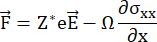
With σxx being the normal stress along the length of the sample and x being the coordinate along the length of the line under test1. As has been shown in other publications, this results in5:

Electromigration generating stress is a well-known phenomenon in the solid-state lines under test.
If = 0 then the mass transport = 0 (and V = 0), the critical product of length l and current density for the onset of electromigration can be related to the materials parameters as follows1:
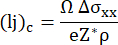
This critical product is of high importance in the design of electrical components or circuits since lines with shorter lengths than the critical length, also called Blech length, are immortal. In the protocol below, the determination of (Ij)c is shown. If the other parameters are known, Z* as an important material quantity can be calculated.
Previously published methods for the measurement of the electromigrated volume use SEM, transmission electron microscopy (TEM), or x-ray microtomography (X)3,4,6,7,8,9.
Using these instruments involves delicate preparation of the samples, such as applying an additional thin metal film on surfaces having a high resistivity in order to reduce the accumulation of charges on the surface during electron beam scanning.
The additional layer on the surface can cause problems, such as changing the electromigration behavior by modifying the mechanical stress at the interface. Charge accumulation, on the other hand, can cause a virtual drift of the sample during a scan, making the data useless.
The operation of SEM, TEM is also more time-consuming and more expensive than the use of a laser scanning microscope. The use of the laser scanning microscope facilitates the investigation of the lines under test at higher temperatures. For SEMs, there also exist some heating stages that are not readily available for all SEMs, are expensive, and are oftentimes custom-made.
With a laser scanning microscope, the measurement uncertainty of the volumes can be in the same range as for SEMs, provided that appropriate equipment is used and meticulous care is taken over the measurement conditions.
During the scan of the surface, multiple values are measured for each point, resulting in a high resolution. Because of the scanning principle of the laser scanning microscope, the limit of the method is not equal to the diffraction limit. This enables the measurement of structures of the lateral size of approximately 120 nm.
Compared to SEM measurements, the height of structures can be measured more easily and precisely with a lot less effort. Determination of the height with an SEM might employ measuring the height of several intersections after preparing these with a focused ion beam (FIB). The FIB can cause abrasion in the vicinity. Because of these preparations, the volume of a void or hillock might not be adequately represented by the SEM measurements, resulting in volume measurements of both methods having a similar accuracy.
Since operating under ambient air conditions, it is possible to operate faster, cheaper and more versatile than using SEM or a TEM.
The method described here can be used if the oxidation of the material during the measurement can be avoided. Oxidation can occur at elevated temperatures because of self-heating of the lines under test. Otherwise, using a SEM or scanning the line under the tests, the geometry of the region of interest first, then applying electromigration stress in an evacuated chamber, and finally scanning the line under tests geometry of the region of interest for the second time is recommended.
If the sample gets moved for stressing in a different environment, care has to be taken to align the sample before and after stressing in the same direction. Aligning removes the need to correct the scanned images for turning. This typically gives more accurate results than correcting the turn by software.
This method uses prepared samples and includes the initial laser scans, stressing the samples under predetermined conditions and making second laser scans of the same regions. From these scans, the electromigrated volumes of several samples are determined by subtraction of the two laser scans. Using the volume data of several samples, the interception of the line of best fit for different lengths is determined. This interception is the Blech length under the conditions used in the experiment. The method has advantages when investigating an electrically conductive material with a high resistivity or a material negatively affected by the sample preparation needed for the other methods.
The geometries of lines under test for electromigration tests vary widely depending on the measurement technique used. The use of a laser scanning microscope is not limited to single lines under test with widths of several µm10 but can be used for all the structures in which changes of the volume caused by electromigration are investigated, such as Blech-structures.
Protocol
1. Choosing the material and making lines under test of the material of interest
- Choose lines under test of the material of interest and assemble these to get access to the region of interest of the line under test with the laser scanning microscope.
NOTE: Lines under test may have geometries used in leading-edge semiconductors or might be bigger and only used for evaluation of electromigration phenomena. Line geometries might be but are not limited to widths of 20-50 µm, thicknesses of 10 nm up to 200 nm, and lengths of 40 µm up to 800 µm. The region of interest depends on the materials used and on the geometry of the test structure, which has to be determined by scanning the whole test structure during the first experiments using strong stressing conditions. All the parts of the test structure showing changes in the volume can be used as the region of interest. - Use encapsulated or not encapsulated lines under test made of the same material having the same cross-section (same height and width) with different lengths. Stress them using the same conditions (current density, temperature, atmosphere, time) to determine the critical length for the onset of electromigration.
- Alternatively, use lines under test with the same length and vary the current density in a small range while stressing with the same temperature in the same atmosphere.
2. Determining the electromigrated volume
- Determine the electromigrated volume for different lengths (multiple data points) or different current densities according to the later steps of the protocol, which describe in detail how to get a single data point.
NOTE: With the method enclosed in this publication, every sample is used to get one data point. - Get one data point
- Use a laser scanning microscope with the highest resolution available.
NOTE: Not all laser scanning microscopes achieve the resolution needed for the method enclosed in this protocol. - Switch on the laser scanning microscope and open the measurement and analytics software. If the measurement software asks, Return to the XY stage origin? click on No.
- Get the samples and an appropriate sample holder to be able to fix the sample onto the stage of the laser scanning microscope so the sample will not move during the scanning process.
- Get an accurate current source and wires for electrical connection. Make sure the current source and the cables work properly.
- Change the height of the stage of the laser scanning microscope and place the sample in the sample holder under the laser scanning microscope. Align the sample parallel to the table of the microscope. Fix the sample so it will not move during measurements.
NOTE: It is possible to pause the experiment at this point. Sometimes, the behavior of samples changes depending on the storage conditions e.g., because of oxidation. Pauses are optional and should be avoided if the samples are expected to change a lot with the conditions they are in for these measurements. - Connect the current source's electrical outlet to the sample or sample holder depending on the setup. Check if the bond wires are still attached to the sample either by using a low current for a short time or by optical inspection.
NOTE: It is possible to pause the experiment at this point. - Adjust the height difference between the objective lens of the laser scanning microscope and the sample to get the sample into focus. Bring the region of interest into focus of the objective lens with the lowest magnification. Either manually or in the Observe window of the measurement software by clicking Auto focus.
NOTE: If necessary move the XY-position of the table to be able to see the region of interest. It is possible to pause the experiment at this point. - Change the objective lens to the next higher magnification and focus on the region of interest. Either manually or in the Observe window of the software by clicking Auto focus.
NOTE: It is possible to pause the experiment at this point. - Repeat changing the objective lens and the focusing until the focused region of interest is visible using the objective lens with the highest magnification, e.g. 150x in the Observe window.
NOTE: If the region of interest is bigger than the region being able to scan with the most accurate settings of the laser scanning microscope use stitching. The protocol does not include explanations of how to proceed with stitching. It is possible to pause the experiment at this point. - Make sure Tools > Measure > Average count is set to 4. Click Options > Auto save, choose a save destination folder, a file name prefix, and a file name sample, and click Ok.
- Go to the Measure window. Select Expert Mode. Use Measurement settings > Surface profile > Super fine (2048 x 1536) > High-accuracy.
NOTE: The names of the settings to get the highest accuracy might be different if another laser scanning microscope is used. - Increase the distance between the objective lens and the sample by clicking upward arrows until the whole window shows the surface is black. Click Set upper pos. Decrease the distance between the objective lens and the sample by clicking downward arrows until the whole surface is visible, and continue clicking downward arrows until the whole window showing the surface is black. Click Set lower pos.
- Click Auto gain and Start measurement to start scanning the surface of the region of interest.
NOTE: In the first experiment using a material and setup, scanning not just the region of interest but all the surface of the line under test from one electrical contact (e.g., bond wire) to the other contact (bond wire) of the sample to the first part only being used for the connection of the sample to the surroundings is necessary to be able to pinpoint where the atoms comprising the new volume come from as they can be from a different part of the sample and to rule out different effects such as thermomigration causing the volume to appear. It is possible to pause the experiment at this point. - Defocus the laser scanning microscope by increasing the distance between the objective and the sample by several mm up to 1 cm by clicking upward arrows multiple times before stressing the sample.
NOTE: This is to avoid damaging the objective lens. Depending on the material of the line under test and the stressing conditions, the line under test will heat up. In some cases, the temperature will reach several hundred degrees centigrade. The distance between the objective lens and the sample is typically shorter than 2 mm during laser scanning. The objective lens would heat up considerably during the experiments if the distance is not increased during stressing. Heating up the objective lens leads to mechanical stress in the lens which might lead to deformation of the lens or other damage to the lens. - Stress the sample with the predetermined conditions (current density, time). Stop the current flow after the predetermined time.
NOTE: The conditions include current density, stressing time, temperature, and length of the line under test. The stressing conditions depend on the material of interest. It is possible to pause the experiment at this point. - Wait 3-5 min after the current stressing. Focus the laser scanning microscope on the region of interest after the sample cools down to room temperature (RT).
NOTE: It is possible to pause the experiment at this point. - Focus again until the sample stops to defocus on its own to be sure not to have drifts in the measured surface because of the temperature changes.
NOTE: It is possible to pause the experiment at this point. - Scan the same area that has been scanned before the current stressing with the same settings according to steps 2.2.10-2.2.13.
NOTE: It is possible to pause the experiment at this point. - Use the analytics software and correct the two images of the region of interest.
- Open the file in the analytics software if it is not opened by clicking File > Open and searching for the correct file.
- Correct the tilt of the samples by clicking Process image> correct tilt to open a window for the correction of the tilt. Use the display image Laser+Optical and the correction method Plane tilt (3 points) to make three points appear in the displayed image.
- Move the lines in a way that most of each of these lines is in the background. Move the three points close to the region of interest. Move these points to match the plane, which is represented by two straight lines in the cross sections, to the background.
NOTE: If the background is not properly represented by a plane, match the plane to the lower edges of the region of interest. - Choose Do not adjust offset height 0 data and Auto adjust height range and click Execute and Close.
- Remove heights caused by the overdrive of the laser scanning microscope by clicking Process image > Height cut level to open the height cut window. Set the cut level to Normal, use Always compliment height 0 data, and click OK.
NOTE: It is possible to pause the experiment at this point. - Trim the image if it is larger than the region of interest and is too big to be evaluated with the software intended for the evaluation. Trim the image so the region of interest is in the center, e.g., 500-pixel x 500-pixel.
- Trim by clicking Process image > Trimming to open the trimming window. Choose the width and height according to the region of interest and move the rectangle for selection to include the region of interest.
NOTE: The ideal would be not having to correct the images at all by aligning the samples perfectly so they have no tilt regarding the sample stage and only scanning a portion of the sample slightly bigger than the region of interest. This ideal type of measurement might not be possible with the equipment available.
- Save the corrected trimmed image. Open the corrected and trimmed image with the analytics software by clicking File > Open and choosing the correct file.
- To export the data in a way to keep the 3D information about the region of interest, e.g., as an ASC file, use the following steps. Click File > Output 3D-CAD data to open the window for selecting the output parameters.
- Use skip amount 1 (no skip) > Actual number display accuracy 10 > XY zoom ratio x1 and Enhance height (%) 100 and choose Surface or use the options with the highest accuracy available. Click Set. Use Point group data to save the uniquely labeled data. After finishing exporting the data, the program will show a window.
- Use unique names to match the data of the measurement before and after current stressing for each region of interest.
NOTE: It is possible to pause the experiment at this point.
- Transfer the data to the evaluation software.
NOTE: Some laser scanning microscopes have software with built-in functions to measure volumes. If this is the case, using the built-in software instead of using the software described in this protocol is an option. - Use a version of the evaluation software mentioned in the Table of Materials and packages mentioned in the Table of Materials and open the program (Supplementary Coding File 1: Laserscan_1.vi).
NOTE: Other software might be used to get the same results. - Click the arrow to start running the program. Open the save path of the asc files intended for use by clicking Open. Load the asc files into the program by choosing the name of the sample in the selection list. Make sure area is selected and click cross and area.
NOTE: If the electromigration occurs for a long time or the electromigration effect is strong in the sample with the chosen conditions, the program might not be able to match the patterns of the images. If this happens, redo a similar measurement with a new sample at lower current densities, shorter times under test, or lower temperature and adjust future experiments accordingly. - Adjust the pattern matching manually if the program does not match the patterns perfectly.
- To add the scale for the height, use the mouse to choose a rectangle belonging to the substrate surface. Look at the two histograms of the heights of the rectangle in the image before and after the current stressing next to the image of the region of interest. Make the shape of these two histograms look normally distributed and as similar as possible.
NOTE: If the histograms look very different, redo the chosen rectangle and vary the rectangle ever so slightly until it is content with the shape of the histogram. - Click the zero button labeled as background to save this height as the background.
- Choose another rectangle on a flat part on top of the line under test.
NOTE: If the region chosen with this rectangle changed during the experiment, redo the rectangle until a region without changes has been chosen. If the region gets too small, e.g., only a few pixels the determination of height will not be accurate. If there is only a really small region that did not change, use an image with more pixels to get a region without changes that is on top of the line under test. - Look at the two histograms next to the image of the surface of the region of interest. Make the shape of these two histograms look normally distributed and as similar as possible.
NOTE: Redo making rectangles that fit all the criteria and also give a good result in the histogram. - Save this value by clicking line under test and click Ok.
NOTE: This data is only saved temporarily for now. - Stop the program by clicking the red stop button and save the height parameters permanently to the program by clicking Edit > Make Current Values Default and File > Save.
NOTE: The program takes the background as a height of zero and the height of the line under test as 1. This will be multiplied by the measured height of the line under test in later steps/in the end. - Click the arrow to start running the program. Evaluate a single hillock (or void) in the region of interest by drawing a rectangle with the left mouse button close to the rim of the hillock (or void) in the IMG compared to the front panel.
- Get as close to the rim of the structure as possible. Improve the selected area using the zoomed version of the structure and zoom into the image, e.g., the one labeled relax crop.
- Adjust the selected hillock (or void) region until the content matches the rim of the rectangle to the hillock (or void).
- Click the save button next to the IMG compare to save the sum of all the pixels (integral) of the volume.
NOTE: It is possible to pause the experiment at this point. - Continue with the next hillock or void in the image. Follow steps 2.2.31 up to 2.2.34 for every hillock (or void) present in the image.
NOTE: It is possible to pause the experiment after saving the integral of every hillock (or void). - Use the volume data and calculate the sum of the volumes of the hillocks (or voids) to get the volume of the electromigrated material in one region of interest under these conditions.
- Convert the determined summed volume (units are pixel x pixel x height) into the cubic meter (m³) by multiplying with the size corresponding to one pixel in meter and the factor for the height of the line under test, including the height of the encapsulating layer.
NOTE: In this work, each pixel is 0.05 µm x 0.05 µm. The height of the line under test, including the height of the encapsulating layer for converting in the cubic meter, can be measured with any suitable measurement technique. - Save the volume and the measurement conditions (length of line under test, current density, temperature, time of current stressing) as one data point.
NOTE: It is possible to pause the experiment at this point.
- Use a laser scanning microscope with the highest resolution available.
- Get more data points by following step 2.2. for lines under test with lengths being different from the lengths used before until at least three data points with the electromigrated volume being different from zero exist. Alternatively get more data points by following step 2.2 for lines with the same length and varying the current density slightly.
- To obtain the critical length for the material of interest and measurement conditions, make a graph with at least three data points - that are not located on either the x-axis or the y-axis - with the electromigrated volume on the y-axis and the length or the current density using the parameter with varied values on the x-axis.
- Determine the line of best fit for the data with the line of best fit having less than two intercept points with the x-axis. Get the intersection of the linear line of best fit for data points with small volumes with the x-axis. This intersection is either l or j of (Ij)c and (Ij)c calculate by multiplying the value of the interception with the current density or length used in the experiment, respectively.
NOTE: Depending on the stressing conditions, the lengths, and the material investigated, the line of best fit can be linear close to the interception or exponential if stressing conditions such as the current density or length are higher.
Results
Figure 1 shows the schematic of a test structure geometry, and Figure 2 shows the schematic of the workflow of the measurements needed to get one data point. To investigate the influence of the length and the existence and the numeric value of the length of the line under test needed for the onset of electromigration the aforementioned protocol was used to gain data for multiple lines under test with different lengths (e.g., 120 µm, 540 µm, and 680 µm) made of molybdenum disilicide and encapsulated by a layer of high-temperature silicon oxide. All the lines under test were manufactured the same way and stressed for the same time of 7 min under ambient air conditions at room temperature (23 °C) with a constant current without narrowing of the line under test while stressing, resulting in a constant current density of 2.26 × 10¹⁰ A/m2, 3.25 × 10¹⁰ A/m2 or 3.44 × 10¹⁰ A/m2.
In the test structures used (encapsulated MoSi2 lines) only the contact region of MoSi2 to aluminum showed changes in the volume. Previous experiments showed no protrusions of any kind through the encapsulation.
The lateral sizes of all the hillocks evaluated with this method were above the size of 200 nm, well above the lateral resolution of the laser scanning microscope.
V = const.lwh
The maximum uncertainty of the measured volume can be estimated via covariance propagation law.
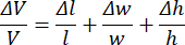
With l being the length, w the width, and h the height. With the measurement uncertainties of the individual dimensions Δl = 50 nm, Δw = 50 nm, and Δh = 12 nm. The uncertainties of the length and the width are taken as the dimensions of one pixel. The uncertainty of the height of Δh = 12 nm has been measured via SEM on the smallest hillock detectable via laser scanning microscope and is in accordance with the uncertainty stated by the manufacturer.
The height of the hillocks (as shown in Figure 3) is usually in the range of 190 nm. The smallest properly detectable hillocks have heights in the range of 34 nm. The lengths and widths are usually in the range of 1 µm for most of the hillocks, as shown in Figure 3.
This causes the uncertainty for a single hillock with a typical hillock size to be
 = 16%
= 16%
and for a small hillock to be
 = 45%.
With the method shown in this protocol, the volume is summed for several hillocks. Typical values for the amount of hillocks summed in one sample are about 9 as shown in Figure 3.
This causes the uncertainty to be:
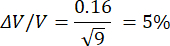
If only average sized hillocks are present in the sample
and
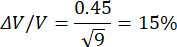
if all the hillocks present in the sample are extremely small.
In reality, small and typically sized hillocks are present in the samples, and the amount of hillocks slightly varies between the samples causing the uncertainty to be between 5% and 15% depending on the exact sizes and numbers of the hillocks.
As can be seen from the representative results shown in this work, the value of the electromigrated volume increases with the increased length of the line under test. The electromigrated volume also increases if stronger stressing conditions, e.g., higher values of current density are used.
If all the volume data independent of the length of the line under test is zero, then stronger stressing conditions (e.g., higher temperatures, longer stressing time, higher current densities, or a combination of these) are needed for the onset of electromigration. Stronger stressing conditions are to be used in further experiments.
Figure 3 shows a region of interest before current stressing on the left-hand side and after current stressing in the middle. The right-hand side of Figure 3 highlights the hillocks after current stressing. Figure 3 shows new hillocks having formed and the growth of protrusions having been present before the current stressing.
Figure 4 shows successful results of the increase of the electromigrated volume with increasing length, including an exponential line of best fit, including all the data points. Figure 4 also shows the results for shorter lengths being used to determine the interception of the linear line of best fit with the x-axis.
Figure 5 shows successful data of the electromigrated volume increasing with an increase of the current density with the length being kept constant at 120 µm and the current density varied in the range the onset of electromigration was observed in previous experiments. Figure 5 also shows the influence of the encapsulating high-temperature silicon oxide. Two different thicknesses of high-temperature silicon oxide (filled circles: 60 nm, unfilled circles: 20 nm) result in two different values for the onset of electromigration regarding the current density. This is caused by the mechanical stress of the encapsulating layers.
Figure 6 shows data that might be ok to use to get a first estimate of electromigration parameters in the material. To get better results, more data with lengths in the range of 150 µm up to 500 µm should be acquired.
Figure 7 shows suboptimal data, which would require testing of lines under test with lengths being between 120 µm and 260 µm as there might be lengths above 120 µm also having an electromigrated volume of 0. If there is a decrease of the volume with an increase of the length of the test structure some of the data is incorrect. Most likely because of errors in the evaluation of the volume, such as errors in the determination of the height scale or errors in finding the rim of the hillocks. If this is the case, having another look at the evaluation of the respective image and reevaluating can be used to get to the bottom of the issue.
Wrong data can also be because of not letting the test structure cool down to room temperature for the second scan. Scanning the same area again and using the new scan for the evaluation is the only option to address the issue. If this issue persists after reevaluating and redoing the scan, it is likely not caused by an error in the evaluation and could be a real effect of the material used.
For lengths slightly above the critical length, the line of best fit can be approximated by a straight line. If the length of the lines under test gets longer, the exponential nature of the line of best fit becomes visible.
The interception with the x-axis was determined to 33.33 µm for stressing with a current density of 3.25 × 10¹⁰ A/m2 resulting in (Ij)c =1.08 × 10⁶ A/m.
From the data of Figure 5 the interception was determined to 3.49 × 10¹⁰ A/m2 and 3.6 × 10¹⁰ A/m2. With the length of the line under test being 120 µm these give values of 4.19 × 10⁶ A/m and 4.2 × 10¹⁰ A/m.
Discrepancy of the measured critical product arises from an increased self-heating of the lines under test with an increase in the current density. The temperature of the lines under test typically increases with increased current density. The temperatures of lines under test of a length of 120 µm stressed for 7 min were determined via measurement of the electrical resistivity for current densities of 2.65 × 10¹⁰ A/m2, 3.24 × 10¹⁰ A/m2, 3.53 × 10¹⁰ A/m2 and 3.85 × 10¹⁰ A/m2 to be 158 °C, 202 °C, 257 °C, and 320 °C, respectively. A dependence of the critical product on the temperature and other factors has been shown before11.
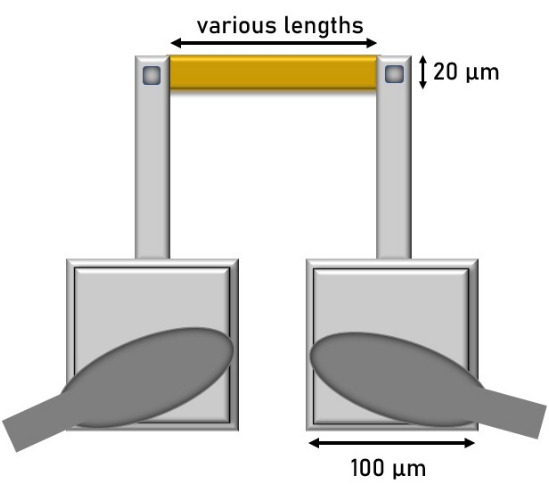
Figure 1: Schematic of a test structure geometry being suited for investigations of electromigration parameters via laser scanning microscope. The golden box is the line under test (in this work made of MoSi2), silver boxes are the electrical supplies (in this work made of aluminum), and the contact pads are shown as stacks of the silver boxes in the region of the bond wires (dark grey). The stacks indicate that the contact pads have a higher layer thickness than the electrical supplies. The small silver boxes on both sides of the line under test are the regions of electrical contact of the electrical supply and the line under test. The dark rim is supposed to symbolize this region having a lower elevation because of the encapsulating layer being opened at this portion to enable electrical contact. Please click here to view a larger version of this figure.
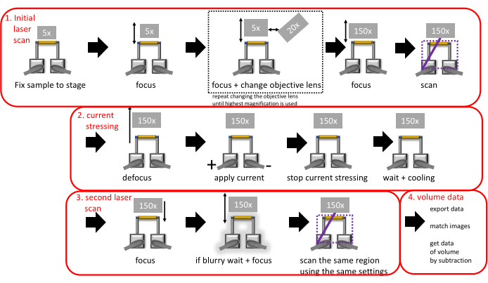
Figure 2: Schematic of the workflow of the measurements needed to get one data point. Please click here to view a larger version of this figure.
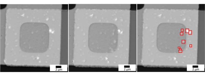
Figure 3: Comparison of the region of interest before and after current stressing. Comparison of the region of interest (in this work, the electrical contact of aluminum with the line under test) before current stressing (left-hand side) and after current stressing (middle) with the hillocks caused by electromigration highlighted on the right-hand side. Please click here to view a larger version of this figure.
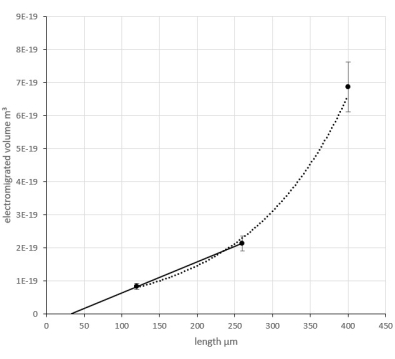
Figure 4: Successful results of electromigrated volume of contact regions of the cathode side depending on the length of the line under test for MoSi2 lines. Representative data (successful results) of the electromigrated volume of contact regions of the cathode side depending on the length of the line under test for MoSi2 lines encapsulated with 60 nm high-temperature silicon oxide, stress under ambient air conditions for 7 min with a current density of 3.25 × 10¹⁰ A/m2. Please click here to view a larger version of this figure.
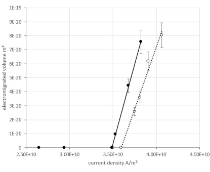
Figure 5: Successful results of electromigrated volume of contact regions of the cathode side depending on the current density for encapsulated lines under test made of MoSi2. Representative data (successful results) of the electromigrated volume of contact regions of the cathode side depending on the current density for encapsulated lines under test made of MoSi2 while stressed at ambient air conditions for 7 min. Filled circles show the data of MoSi2 lines under test encapsulated with 60 nm high-temperature silicon oxide. Unfilled circles show the data of MoSi2 lines under test encapsulated with 20 nm high-temperature silicon oxide. Please click here to view a larger version of this figure.
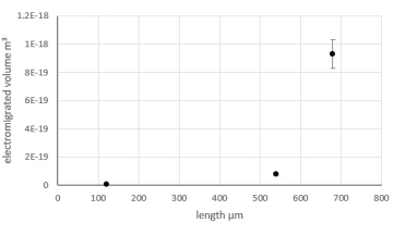
Figure 6: Valid data. Representative data (data is ok to use) of the electromigrated volume of contact regions of the cathode side depending on the length of the line under test for MoSi2 lines encapsulated with 60 nm high-temperature silicon oxide, stress under ambient air conditions for 7 min with a current density of 2.56 × 10¹⁰ A/m2. Please click here to view a larger version of this figure.
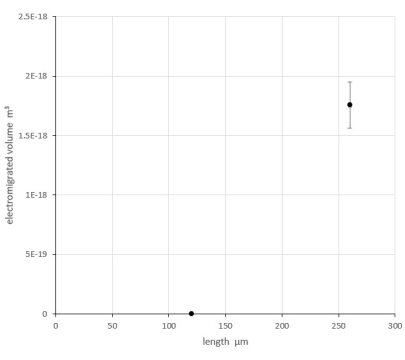
Figure 7: Suboptimal data. Representative data (suboptimal data) of the electromigrated volume of contact regions of the cathode side depending on the length of the line under test for MoSi2 lines encapsulated with 20 nm high-temperature silicon oxide, stressed under ambient air conditions for 7 minutes with a current density of 3.44 × 10¹⁰ A/m2. Please click here to view a larger version of this figure.
Supplementary Coding File 1: Laserscan_1.vi. Please click here to download this File.
Discussion
The protocol outlined here can be used to robustly and reproducibly get data on the electromigrated volume of electrically conductive materials. The materials and the equipment available have to meet certain criteria, as mentioned above in the steps of the protocol or in "NOTEs" to be able to use this method for the evaluation of the electromigration.
Critical parts of the protocol are making sure the sample cooled down to room temperature for the measurement after current stressing. Not cooling down to room temperature will introduce errors to the surface scan because of the temperature change during the scan and will give a faulty determined surface and, therefore, a faulty determination of the volume.
Another important part is choosing adequate background and height of the line under test for determining the height factor in the evaluation program. If this is done incorrectly, the volume will be wrong. Other critical parts are measuring at least three samples that give values for the volume that are different from zero.
If the data for the scan after current stressing does not look good and has not been noticed before doing the evaluation, it is possible to scan again using the same parameters as for the first scan. If this becomes necessary, make sure to be able to avoid turning the sample either by aligning the sample under the laser scanning microscope the same way as before or by correcting this via software. For other methods of troubleshooting, have a look at the notes.
Modifications of the method involve using a heating stage for the sample similar to other experimental methods employing a heating stage11, taking the sample out of the sample holder to stress under different conditions such as elevated temperatures in an oven or other surrounding media (liquids or gases) which cannot be done while the sample is under the laser scanning microscope.
Measurements under different conditions, e.g., temperatures, enable the use of this method of determining the volume to be used to calculate other electromigration parameters such as the effective ion charge or the activation energy. The calculations of the effective ion charge use the electromigrated volume as the starting point. The means of determination of the volume are not important for the calculation. Calculations are done the same way as for determining the effective ion charge by using electromigrated volumes measured via SEM2,3,4.
As stated in the equations before, the electromigrated volume depends on the diffusion. The diffusion exponentially depends on the activation energy of the particular process12. This enables the use of an Arrhenius plot of over to get the activation energy from the linear slope. The method can also be used to determine volume changes in Blech structures and to calculate the drift velocity the same way as shown for volumes determined via SEM11.
This method can only be used if hillocks or voids are accessible to the laser scan of the surface. This makes the method unsuited for evaluating the volume change caused by submerged voids. The laser scanning microscope is less sensitive to changes in the volume than the smallest changes being detectable via SEM and TEM. If the electromigrated volume is too small using a laser scanning microscope will not give any useful results.
Compared to investigations using SEM or TEM, it is easier to include a heating stage in the setup of the laser scanning microscope because they typically have to be custom-made7,11,13,14.
Disclosures
The authors have nothing to disclose.
Acknowledgements
This research was funded by the "German Federal Ministry for Economics Affairs and Climate Action" in the project "EMIR" funding code 49MF190017.
Materials
| Name | Company | Catalog Number | Comments |
|---|---|---|---|
| Current source/2602B System Source Meter | Keithley | 2602B | Any type of current source can be used. |
| JKI VI Package Manager | NI | 781838-35 | https://www.ni.com/de-de/shop/product/jki-vi-package-manager.html? srsltid=AfmBOorzYPY4B8 hlGIUIYl3PJoBwb8o8PeV MsBfM9YcFasnBIhEWwBpd |
| Labview 2024 Q1 Full | NI | 784522-35 | Evaluation software option (https://www.ni.com/de-de/shop/product/labview.html?partNumber=784522-35) |
| Labview 2024 Q1 Pro | NI | 784584-35 | Evaluation software option (https://www.ni.com/de-de/shop/product/labview.html?partNumber=784522-35) |
| Laser scanning micrsoscope VK-X200 series | Keyence | VK-X200 no longer available for purchase. Available option VK-X3100. Laser scanning microscope with wavelength of 408 nm. | |
| NI Vision Development Module | NI | 788427-35 | https://www.ni.com/de-de/shop/product/vision-development-module.html?srsltid=AfmBOoq2S8kYVmV1CK6 xSovMHTELtQHE2neD oM2RrEnibd2AuyzkWvuS |
| Objective lens, CF Plan Apo 150x/ 0.95; ∞/0 EPI; OFN25 WD 0.2 | Nikon | BZ10123016 | https://spwindustrial.com/nikon-cf-plan-apo-150x-0-95-0-wd-0-2mm-epi-objective/ |
| VK Analyse-Modul Version 3.3.0.0 | Keyence | Analytics software supported by the laser scanning microscope. No longer available for purchase. New laser scanning microscope uses newer software. | |
| VK Viewer Version 2.2.0.0 | Keyence | Measurement software supported by the laser scanning microscope. No longer available for purchase. New laser scanning microscope uses newer software. |
References
- Somaiah, N., Kumar, P. Inverse blech length phenomenon in thin-film stripes. Phys Rev Appl. 10 (5), 054052(2018).
- Huynh, Q. T., Liu, C. Y., Chen, C., Tu, K. N. Electromigration in eutectic SnPb solder lines. J Appl Phys. 89 (8), 4332-4335 (2001).
- Lee, T. Y., Tu, K. N., Kuo, S. M., Frear, D. R. Electromigration of eutectic SnPb solder interconnects for flip chip technology. J Appl Phys. 89 (6), 3189-3193 (2001).
- Lee, T. Y., Tu, K. N., Frear, D. R. Electromigration of eutectic SnPb and SnAg3.8Cu0.7 flip chip solder bumps and under-bump metallization. J Appl Phys. 90 (9), 4502-4508 (2001).
- Ho, C. E., Hsieh, W. Z., Yang, C. H., Lee, P. T. Real-time study of electromigration in Sn blech structure. Appl Surf Sci. 388, 339-344 (2016).
- Chang, Y. W., et al. Study of electromigration-induced formation of discrete voids in flipchip solder joints by in-situ 3D laminography observation and finite element modeling. Acta Mater. 117, 100-110 (2016).
- Besser, P. R., Madden, M. C., Flinn, P. A. In situ scanning electron microscopy observation of the dynamic behavior of electromigration voids in passivated aluminum lines. J Appl Phys. 72 (8), 3792-3797 (1992).
- Doan, J. C., Lee, S. -H., Bravman, J. C., Flinn, P. A., Marieb, T. N. Void nucleation on intentionally added defects in Al interconnects. Appl Phys Lett. 75 (5), 633-635 (1999).
- Kelly, M. B., Niverty, S., Chawla, N. Electromigration in bi-crystal pure Sn solder joints: elucidating the role of grain orientation. J Alloys Compd. 818, 152918(2020).
- Influences of the microstructure on the drift velocity of electromigrating aluminum through molybdenum disilicide thin films. Schädel, M., Baldauf, J. SMSI 2021 Conference - Sensor and Measurement Science International, , (2021).
- Straub, A. Factors Influencing the Critical Product in Electromigration. , University of Stuttgart, Stuttgart. (2000).
- Scorzoni, A., Neri, B., Caprile, C., Fantini, F. Electromigration in thin-film interconnection lines: models, methods and results. Mater Sci Rep. 7 (4-5), 143-220 (1991).
- Verma, S. K., Raynaud, G. M., Rapp, R. A. Hot-stage scanning electron microscope for high-temperature in-situ oxidation studies. Oxid Met. 15 (5/6), 471-483 (1981).
- Heard, R., Huber, J. E., Siviour, C., Edwards, G., WilliamsonBrown, E., Dragnevski, K. An investigation into experimental in situ scanning electron microscope (SEM) imaging at high temperature. Rev Sci Instrum. 91 (6), 063702-063814 (2020).
Reprints and Permissions
