Organic Light Emitting Diode (OLED) devices offer superior display quality with better contrast while propounding environmental benefits by lower energy consumption. Here, a simple strategy for the solution-processed OLED device fabrication is presented in a sequential manner.
A subscription to JoVE is required to view this content. Sign in or start your free trial.
Method Article
Step-by-Step Guide for Harnessing Organic Light Emitting Diodes by Solution Processed Device Fabrication of a TADF Emitter
* These authors contributed equally
In This Article
Summary
Abstract
The demand for energy-efficient light sources has witnessed a significant surge in the recent era, due to the increasing awareness towards environmental concerns and climate change. Organic Light Emitting Diodes (OLEDs) offer superior display quality, energy efficiency, and sustainability, which makes them an ideal choice for eco-conscious consumers and reduced carbon footprint-based industries. The thinner and more flexible OLEDs have revolutionized the field of smartphones, televisions, automotive displays, and wearable gadgets. Here, in this paper, an efficient OLED device is fabricated starting from the synthesis of a donor-acceptor-based emitter, followed by its purification. The organic synthesis process is explained briefly. For purification, firstly, the product mixture is purified by column chromatography, and then it is sublimed using a temperature gradient vacuum sublimation set-up to obtain a high-purity compound. The ultimate goal is to make a multi-layered OLED device that needs ultra-high-purity emitters. Making an efficient OLED needs precision and expertise; thus, showcasing a detailed step-by-step protocol is important to the science community. Here, the details about the solution-processed OLED device fabrication is unfolded in four steps (substrate cleaning, spin coating of layers, thermal evaporation of layers, and device performance measurement). First, the substrates need to be cleaned using a well-established protocol. Next, the layered architecture is obtained by spin coating and thermal deposition of desired materials to the required thickness. The thermal evaporation is done using a high vacuum thermal evaporator with an integrated glove box setup. Finally, to obtain the device's performance, measurements are to be carried out in a dark environment. This comprehensive work will provide in-depth knowledge of device fabrication and inspire more researchers towards decorating this world with OLEDs.
Introduction
With the increasing modernization, the rate of energy consumption has brimmed over, which has compelled the emergence of several energy-efficient sources. Although it is often unrealized, lighting is one of the major power-consuming fields. According to a report published by the United Nations Environment Program (UNEP) in 20171. Lighting consumes 15-19% of global electricity1,2 and emits around 5% of greenhouse gases in the world1,3. If this issue is left unattended, then electricity consumption for lighting will increase manyfold by 20301,4, significantly impacting climate change due to global warming. Thus, the development of energy-efficient lighting technologies5 holds immense promise towards a sustainable environment.
Organic light-emitting diode (OLED) devices have made a revolution in the field of display and lighting, offering improved display quality along with high energy efficiency6,7. Apart from this, it also offers the required thinness, flexibility, high contrast, and wide viewing angles. Due to all these benefits, the utility of OLED materials is gradually increasing in various applications, including smartphones, televisions, wearable devices, and automotive lighting systems8. OLEDs use organic compounds as the emissive layers, and they emit light upon the radiative recombination of holes and electrons9,10,11. The development of OLED devices has been advanced through three generations of emitter materials12. The first one is fluorescent materials, which can harvest only the singlet excitons, theoretically leading to the Internal Quantum efficiency (IQE) of 25%. The second-generation OLEDs employ phosphorescent emitters to access all the singlet and triplet excitons, due to efficient spin-orbit coupling, all the triplet electrons can also be harvested, leading to 100% IQE13,14. However, these complexes contain heavy metals like iridium (Ir) or platinum (Pt), which raise environmental concerns and cost issues. Thereafter comes the third generation of OLEDs, comprising thermally activated delayed fluorescence (TADF) emitters15,16,17,18,19.
TADF molecules exhibit a small energy gap between triplet and singlet excited states, enabling reverse intersystem crossing (RISC) activated by thermal energy and achieving a theoretical IQE of 100%20. Designing a TADF molecule holds the strategy to attach a donor and an acceptor group with or without the help of a core unit. A suitable core supports efficient electronic coupling between the donor and acceptor groups. Electron-rich groups (for example, carbazole, phenoxazine, phenothiazine, triphenylamine) are generally used as donors, whereas electron-deficient groups (for example, triazine, oxadiazole, benzophenone, or cyano groups) function as acceptors21,22,23,24,25,26,27. TADF emitters possess a small singlet-triple energy gap (ΔEST), which helps in facilitating Reverse Intersystem Crossing (RISC)28. Here, in this work, we prepare a D-A type TADF molecule, which will further be utilized to make a green emissive OLED device28.
Multilayered OLEDs have significantly advanced OLED technology by improving the performance metrics compared to single-layered devices. A multi-layered OLED device contains several organic layers, each of which serves some specific function29,30. The device performance can be tailored by altering the material, thickness, and concentration of each layer. The materials of these layers are chosen according to their energy level of highest occupied molecular orbital (HOMO) and lowest unoccupied molecular orbital (LUMO). These organic layers remain sandwiched between the two electrodes (cathode and anode). Once connected to the circuit, electrons flow from the HOMO of the emissive molecules toward the voltage source through the anode, creating a hole. Whereas the voltage source supplies electrons to the LUMO of the molecule through the cathode. These opposite charges travel across the device and recombine in the emissive layer, and the radiative recombination of the excitons emits photons. Depending upon the emissive layer materials and their HOMO-LUMO energy gap, the emission color can vary29. It is desired that the recombination happens in the emissive layer (EML); for that, an optimized device structure is required. If the layers and their thickness are not properly optimized, the recombination may get shifted, resulting in poor device performance.
The multi-layered device fabrication can be of two types, either by vacuum thermal deposition or solution processing. Here, in this paper, a detailed method is presented for the device fabrication of a TADF emitter using the solution-processed method (in which spin coating is made for the first three layers, followed by the vacuum deposition of the next three layers). The solution-processed device fabrication process attracted more attention due to being cost-effective, highly scalable, and environmentally sustainable. Moreover, the material wastage is comparatively less than vacuum thermal evaporation. Solution-processed material can be deposited at room temperature, which makes it a suitable choice, enabling fabrication on flexible and heat-sensitive substrates. In fact, for those molecules with low thermal stability, the device can be made only by this method. However, there are a few things to consider prior to the fabrication. The solubility of the emitter, stability, and uniformity of the film need to be checked.
Here, we prepared a D-A type TADF molecule, which will further be utilized to make a green emissive OLED device28. Firstly, the synthesis strategy for the TADF emitter 2BPy-oTC is discussed in a nutshell; the detailed discussion is already reported in the earlier paper by our group28. Further, the synthesized material was purified by column chromatography, and to obtain high-purity material, it was sublimed using a temperature gradient high vacuum sublimation setup. The purification step is extremely necessary, as any trace impurity will affect the device's performance. Next, for fabricating the device, indium tin oxide (ITO) patterned glass substrates were taken and cleaned. Cleaning of the substrates is very important31. The ITO-coated substrates were cleaned thoroughly by sonicating with soap solution, ultrapure water, and organic solvents, followed by ozone cleaning. Next, the Hole Injection Layer (HIL) was spin-coated on top of the ITO substrate (anode), and the polymeric layer of poly(3,4-ethylenedioxythiophene) polystyrene sulfonate (commonly known as PEDOT: PSS) was taken as HIL. The Hole Transport Layer (HTL) was spin-coated on top of HIL. This layer helps in the migration of the holes toward the emissive layer. Poly(9-vinylcarbazole) (PVK), having a similar HOMO energy level to PEDOT: PSS, was used as HTL. Further, the Emissive layer (EML) was spin-coated on top of HTL. To avoid concentration quenching in most of the TADF-based devices, the emitter molecule is dispersed in a host matrix. In this study, 10 wt% of 2BPy-oTC was taken in N,N′-Dicarbazolyl-4,4′-biphenyl (CBP) host, which is a well-known host for green emitter32,33,34. Then these fabricated substrates were loaded into the thermal evaporator. The Electron Transport Layer (ETL) and Electron Injection Layer (EIL) were deposited by thermal evaporation. This thermal evaporation demands precise control of deposition rate under a high vacuum environment. 2,2′,2"-(1,3,5-benzinetriyl)-tris(1-phenyl-1H-benzimidazole) (TPBi) was deposited as the ETL, which helps to transfer the electrons from EIL to the EML, and 8-Hydroxyquinolinolato-lithium (Liq) was used as EIL, which injects the electrons into the device architecture through a tunneling effect. Finally, 100 nm of aluminum was deposited with a cathode mask. So, the overall device structure is as follows - ITO/ PEDOT:PSS (30 nm)/ PVK (30 nm)/ 10 wt% 2BPy-oTCz in CBP (30 nm)/ TPBi (50 nm)/ Liq (2 nm)/ Al (100 nm).
Access restricted. Please log in or start a trial to view this content.
Protocol
NOTE: Devices are very sensitive to dust and foreign particles; any kind of impurity can alter the actual performance of the emitter and can potentially lead to non-functioning or short circuits in the device. So, these need to be made in a clean place with utmost precautions. It is advised to prepare the devices inside the glove box with a controlled moisture and oxygen environment (oxygen and moisture level 0.1 ppm).
1. Emitter synthetic strategy
- Find a suitable design for a donor-acceptor-based TADF molecule with the help of a literature survey. Scrutinize the proposed structure through theoretical calculations; if it satisfies the requirements, proceed with the synthesis. Generally, if the molecule has ΔEST < 0.2 eV, then it can show TADF property35,36,37.
NOTE: For this study, the molecule 2BPy-oTCz was taken as the emitter28. Here, the electron-rich 3,6-di-tert-butyl-9H-carbazole (TC) acts as the electron donor unit, whereas phenyl(pyridine-2-yl)methanone (2BPy), having an attached electronegative carbonyl group, acts as the acceptor unit. The synthetic route is shown in Figure 1, and the detailed characterizations are provided in a previous publication28.
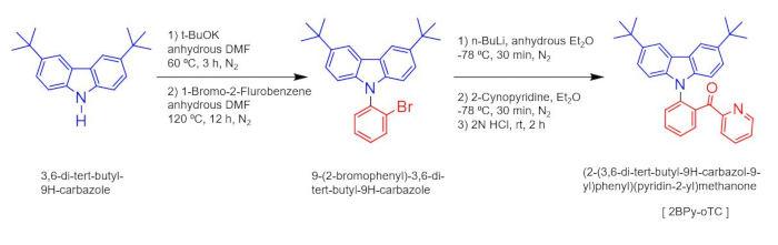
Figure 1: Synthesis process for the emitter 2BPy-oTC. Please click here to view a larger version of this figure.
2. Purification of the emitter
- Purify the synthesized compound by column chromatography. Use ethyl acetate/ n-hexane mixture as the eluent.
- Obtain a high-purity compound (>99.9%) by subliming the compound using a temperature gradient high vacuum thermal sublimation setup. This segregates the impurity from the compound based on their sublimation temperature.
3. Solution processed device fabrication
NOTE: Here, in this paper, the steps of making a solution processed device with the emitter 2BPy-oTC is demonstrated. The schematic image of the device architecture and the molecular structures are given in Figure 2.
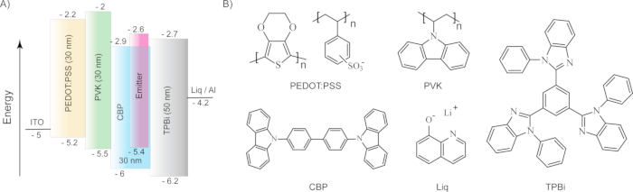
Figure 2: Molecular layers used for the device fabrication. (A) Device architecture showing the thickness and HOMO-LUMO energy levels of all the layers. (B) Molecular structure of PVK, CBP, Liq, and TPBi. Please click here to view a larger version of this figure.
- Substrate cleaning
- To make good devices, substrates need to be cleaned thoroughly. Take patterned ITO glass substrates.
NOTE: These patterned ITO substrates can be of different types; it can contain 2/4/6/8 pixels and the size of the pixels may also vary. In this paper, substrates containing 6 pixels were taken, and after the device fabrication, the area of 1 pixel is about 4.5 mm2. - Keep the substrates in a substrate holder for cleaning. Then submerge into acetone (in a beaker) and sonicate in an ultrasonic bath for 10 minutes (keep temperature around 40 °C).
- Sonicate the substrates in isopropyl alcohol, followed by 1% (v/v) Helmanex III soap water, ultrapure water, acetone, and isopropyl alcohol in sequence for 10 minutes each. Keep the temperature around 40 °C, and proper cleaning is required to remove any dust and organic residues from the substrates.
- Take out the substrates and then dry with a nitrogen gun. After that, identify the ITO side on the substrate by checking the conductivity using a multimeter, and then clean the ITO surface by using a UV ozone cleaner.
- To make good devices, substrates need to be cleaned thoroughly. Take patterned ITO glass substrates.
- Spin coating of HIL, HTL, and EML
- To spin coat the hole injection layer (HIL) on top of the ITO surface, firstly filter the commercially available PEDOT:PSS through a 0.45 µm PTFE (Polytetrafluoroethylene) syringe filter38 into a vial. Cover the conducting top surface of the substrates with the filtered PEDOT: PSS.
- PEDOT:PSS contains water; coat it outside of the glove box, otherwise, the moisture level will increase inside the glove box.
NOTE: For this work, a 30 nm thick layer was spin-coated with a rpm of 5000 and an acceleration of 2000 rotation/s, duration 60 s. Optimize the thickness of this HIL layer according to the need. - Keep the coated substrate on a hot plate at 140 °C for about 20 min for annealing. Wipe the sides and bottom of the substrate using a wet swab or lint-free tissue. Put the substrates inside the glovebox after annealing.
- Inside the glove box, spin coat 30 nm of PVK (10 mg/mL solution in chlorobenzene) as a Hole Transport Layer (HTL), on top of HIL39 with rpm of 4000 and acceleration of 2000 rotation/s, duration 60s.
- Again, keep it on a hot plate at 140 °C for about 20 min for annealing.
NOTE: As the boiling temperatures of water and chlorobenzene are 100 °C and 132 °C, respectively, the annealing temperature was kept at 140 °C, which is above these boiling temperature values. - To spin coat the EML, filter the emitter embedded host solution through a 0.45 µm PVDF syringe filter into a glass vial. Spin-coat a 30 nm layer with rpm of 3000 and acceleration of 1500 rotation/s, duration 60 s.
NOTE: In this work, 10 wt% of 2BPy-oTC in CBP Host was taken as the EML (9 mg host and 1 mg emitter in 1 mL Toluene).- To make 10 wt% of the emitter, firstly prepare 10 mg/mL stock solutions in toluene of both the emitter and host in separate glass vials. Sonicate the emitter vial and heat the host vial at 70 °C to make homogeneous solutions. Now add host: emitter in a 9:1 ratio to get a 10 wt% emitter solution.
- Wipe the sides and bottom of the ITO-patterned substrate with toluene and transfer it to the thermal evaporator on a metallic substrate holder (image attached in SI).
- Preparation of the evaporation chamber and evaporation of organic layers.
Deposit the ETL, EIL, and cathode layer by vacuum thermal deposition. Deposit the required thickness of the layers by controlling the evaporation rates and time. Evaporate 50 nm TPBi, 2 nm Liq, and 100 nm of aluminum to complete the device fabrication.- Turn on the Evaporator and the chiller (for water circulation).
- Keep the sublimed grade ETL, EIL, and Cathode materials in respective quartz crucibles for thermal evaporation.
NOTE: 2,2′,2"-(1,3,5-benzinetriyl)-tris(1-phenyl-1H-benzimidazole) (TPBi) was taken as ETL, 8-Hydroxyquinolinolato-lithium (Liq) was taken as EIL, and aluminum was taken as the cathode material in this study. Figure 3 shows that a maximum of 10 materials can be loaded in the thermal evaporator for depositing different materials. - Check the lifetimes of all the sensors before starting evaporation. After placing the substrates inside the vacuum chamber, lock the door and turn on the vacuum pump. It will take around 1 hour to reach the vacuum. When the vacuum reaches 10-6 mbar, start the evaporation process.
NOTE: Check crystal lifetimes; they should be above 80, otherwise change the sensor crystal. The time needed to reach the vacuum may vary according to the capacity of the pump. - To ensure homogeneous deposition, start the in-plane rotation of the substrate plate.
- Preheat the TPBi crucible by switching on the power to the TPBi crucible. Control the evaporation rate by controlling the current flow. Once the rate stabilizes around 1-1.5 Å/s, then open the shutter for deposition.
- After evaporating 50 nm TPBi, close the shutter to stop deposition. Reduce the heating by reducing the current flow. Wait until the crucible cools down.
- In a similar way, for EIL, preheat the Liq crucible by switching on the power to the Liq crucible. Once the evaporation rate stabilizes around 0.2 Å/s, then open the shutter for deposition.
- After evaporating 2 nm of Liq, close the shutter to stop deposition. Reduce the heating by reducing the current flow. Wait until the crucible cools down.
- Turn off the rotation of the substrate plate.
- As both the organic layers are deposited, it is time for the evaporation of aluminum (for the cathode). Change the mask to deposit Aluminum.
NOTE: Generally, two different masks are kept in all setups, one for depositing organic layers and the other for depositing cathode materials. - Turn on the substrate plate rotation for homogeneous deposition and set it to 18 rpm.
- Preheat the Aluminum boat by switching on the power to the Aluminum boat. Once the evaporation rate stabilizes around 2-3 Å/s, then open the shutter for deposition.
- After evaporating 100 nm Al, close the shutter to stop deposition. Reduce the heating by reducing the current flow. Wait until the boat cools down. The glow of hot aluminum is given in SI.
- Turn off the rotation.
- Wait 45-60 min, so that the particles inside the chamber settle down. Remove the devices from the evaporator through the glove box.
- Measurement of device parameters
- Calibrate the OLED measurement setup.
- Keep the device on a measuring setup. Make sure the connections between the cathode and the anode are correct.
- Measure the characteristic plots of the device by changing the voltage from 0 to 20 V, in a step increment of 0.5 V, in a dark environment with the help of a source meter and a multimeter. Use a silicon photo detector to detect the signal.
- On the other hand, to obtain EL emission, measure the luminescence at different voltages in a dark environment with the help of a fluorescence spectrophotometer. Choose the emission window of 300-800 nm.
- Using OLED measurement software, with the input values of known pixel area, distance between the device and the photodetector, and gain of the photodetector, the correct device parameters can be obtained. Current Density (J), External Quantum Efficiency (EQE), Luminous Efficiency (ƞP), Current Efficiency (ƞL), and Luminance (L) can be calculated.
Access restricted. Please log in or start a trial to view this content.
Results
Figure 3A shows the arrangement of all the crucibles (or boats) inside the thermal evaporator and the materials used in their respective positions. The setup contains 10 boats, which means at most 10 different materials can be loaded. Figure 3B shows the position of all six sensors. These Quartz Crystal Microbalance (QCM) sensors help to determine the real thickness values of evaporated layers.
Access restricted. Please log in or start a trial to view this content.
Discussion
The above procedure serves as a comprehensive guide for the synthetic strategy of a TADF molecule, purification, solution-processed device fabrication, and characterization of OLEDs. The OLED device was fabricated by facile solution-processing40 of the emissive layer. This results in low cost and easy control of the weight percentage of the host in the emissive layer. This method also allows easy scalability of the device and facile integration to flexible substrates, along with better control ove...
Access restricted. Please log in or start a trial to view this content.
Disclosures
The authors disclose no conflict of interest.
Acknowledgements
Prime Minister Research Fellowship (PMRF) is thankfully acknowledged by S.I.C. and S.C. for the doctoral fellowship. S.B. thanks to IISc-Institute of Eminence (IoE) Postdoctoral Fellowship. University Grants Commission (UGC) and Ministry of Education (MoE) are acknowledged by S.H.N. and N.Y., respectively, for their doctoral fellowship. P.R. acknowledges financial support from the Council of Scientific and Industrial Research (CSIR) [Grant code - 01WS(031)/2023-24/EMR-II/ASPIRE].
Access restricted. Please log in or start a trial to view this content.
Materials
| Name | Company | Catalog Number | Comments |
|---|---|---|---|
| 13 mm X 0.22 μm PVDF syringe filter | BSB Pharma | BSBPTF1345 | |
| 13 mm X 0.45 μm PTFE syringe filter | BSB Pharma | BSBPV1345 | |
| 2,2′,2"-(1,3,5-benzinetriyl)-tris(1-phenyl-1H-benzimidazole) (TPBi) | BLD Pharma | BD234896 | Sublimed |
| 8-Hydroxyquinolinolato-lithium (Liq) | BLD Pharma | BD446731 | Sublimed |
| Acetone | Purechem | used as such | |
| Aluminum pellet | Kurt J. Lesker | EVMAL50EXQD | 99.999% pure |
| Chlorobenzene | Spectrochem | 10342 | >99% puriss AR |
| Hellmanex III soap solution | Sigma -Aldrich | Z805939 | used 1% (v/v) soap solution |
| Isopropyl alcohol | Purechem | used as such | |
| ITO patterned Glass Substrate | Zhuhai Kaivo Optoelectronic Technology Co.,Ltd. | Item no. 004-1520-SK | Sheet resistance<17ohm/sq, size=15*20*1.1mm, Transmittance>82% |
| N,N′-Dicarbazolyl-4,4′-biphenyl (CBP) | BLD Pharma | BD21599 | Sublimed |
| PEDOT:PSS | Ossila (bought) | Clevios P VP AI 4083 | |
| Poly(9-vinylcarbazole) (PVK) | Sigma -Aldrich | 182605 | average Mw ~1,100,000, used as such |
| Toluene | Spectrochem | 52035 | Spectroscopy Grade |
References
- Accelerating the Global Adoption of ENERGY-EFFICIENT LIGHTING. UN Environment-Global Environment Facility, United for Efficiency (U4E). , United Nations Environment. (2017).
- Hafezparast, N. M., Olsson, T., Fischl, G., Aries, M. Smart versus conventional lighting in apartments - Electric lighting energy consumption simulation for three different households. Energy Build. 244, 111009(2021).
- Filonchyk, M., Peterson, M. P., Zhang, L., Hurynovich, V., He, Y. Greenhouse gases emissions and global climate change: Examining the influence of CO2, CH4, and N2O. Sci Total Environ. 935, 173359(2024).
- Pode, R. Organic light emitting diode devices: An energy efficient solid state lighting for applications. Renewable Sustainable Ener Rev. 133, 110043(2020).
- Thejo, N. K., Dhoble, S. J. Organic light emitting diodes: Energy saving lighting technology - A review. Renewable Sustainable Ener Rev. 16 (5), 2696-2723 (2012).
- Izawa, S., et al. Blue organic light-emitting diode with a turn-on voltage of 1.47 V. Nat Commun. 14 (1), 5494(2023).
- Tang, C. W., Vanslyke, S. A. Organic electroluminescent diodes. Appl Phys Lett. 51 (12), 913-915 (1987).
- Zou, S. J., et al. Recent advances in organic light-emitting diodes: Toward smart lighting and displays. Mater Chem Front. 4 (3), 788-820 (2020).
- Liu, S., Xie, W., Lee, C. S. Organic light-emitting diodes, what's next. Next Nanotechnol. 1, 100003(2023).
- Jou, J. H., Kumar, S., Agrawal, A., Li, T. H., Sahoo, S. Approaches for fabricating high efficiency organic light emitting diodes. J Mater Chem C. 3 (13), 2974-3002 (2015).
- Karzazi, Y. Organic Light Emitting Diodes: Devices and Applications. J Mater Environ Sci. 5 (1), 1-12 (2014).
- Dos Santos, J. M., et al. The Golden Age of Thermally Activated Delayed Fluorescence Materials: Design and Exploitation. Chem Rev. 124 (24), 13736-14110 (2024).
- Xiao, L., et al. Recent Progresses on Materials for Electrophosphorescent Organic Light-Emitting Devices. Adv Mater. 23 (8), 926-952 (2011).
- Lee, S., et al. Deep-Blue Phosphorescence from Perfluoro Carbonyl-Substituted Iridium Complexes. J Am Chem Soc. 135 (38), 14321-14328 (2013).
- Hong, G., et al. A Brief History of OLEDs-Emitter Development and Industry Milestones. Adv Mater. 33 (9), e2005630(2021).
- Adachi, C., Sandanayaka, A. S. D. The leap from organic light-emitting diodes to organic semiconductor laser diodes. CCS Chem. 2 (4), 1203-1216 (2020).
- Bizzarri, C., Spuling, E., Knoll, D. M., Volz, D., Bräse, S. Sustainable metal complexes for organic light emitting diodes (OLEDs). Coordinat Chem Rev. 373, 49-82 (2018).
- Uoyama, H., Goushi, K., Shizu, K., Nomura, H., Adachi, C. Highly efficient organic light-emitting diodes from delayed fluorescence. Nature. 492 (7428), 234-238 (2012).
- Zhang, Q., et al. Efficient blue organic light-emitting diodes employing thermally activated delayed fluorescence. Nat Photonics. 8 (4), 326-332 (2014).
- Chen, X. K., Kim, D., Brédas, J. L. Thermally Activated Delayed Fluorescence (TADF) Path toward Efficient Electroluminescence in Purely Organic Materials: Molecular Level Insight. Acc Chem Res. 51 (9), 2215-2224 (2018).
- Wang, Z., et al. Carbazole-based thermally activated delayed fluorescent emitters for efficient pure blue organic light-emitting diodes. Org Electron. , 118-106795 (2023).
- Tsiko, U., et al. TADF quenching properties of phenothiazine or phenoxazine-substituted benzanthrones emitting in deep-red/near-infrared region towards oxygen sensing. Dyes Pigments. 197, 109952(2022).
- Chen, G., et al. Triphenylamine-Functionalized Multiple-Resonance TADF Emitters with Accelerated Reverse Intersystem Crossing and Aggregation-Induced Emission Enhancement for Narrowband OLEDs. Adv Funct Mater. 33 (12), 2211893(2023).
- Braveenth, R., Chai, K. Y. Triazine-acceptor-based green thermally activated delayed fluorescence materials for organic light-emitting diodes. Materials. 12 (16), 2646(2019).
- Lee, J., et al. Oxadiazole- and triazole-based highly-efficient thermally activated delayed fluorescence emitters for organic light-emitting diodes. J Mater Chem C Mater. 1 (30), 4599-4604 (2013).
- Bas, E. E., Ulukan, P., Monari, A., Aviyente, V., Catak, S. Photophysical Properties of Benzophenone-Based TADF Emitters in Relation to Their Molecular Structure. J Phys Chem A. 126 (4), 473-484 (2022).
- Hou, B., Liu, M., Li, Y., Pan, Y., Yang, B. Effect of cyano substitution in TADF molecules on luminescence properties: A theoretical study. Chem Phys. 575, 112080(2023).
- Yadav, N., Deori, U., Manna, A. K., Rajamalli, P. Regulating Spatial Configuration in Donor-π-Acceptor for through-Space Exciton Transfer: Concentration-Independent Emitter for OLEDs. Adv Opt Mater. 13 (9), 2402820(2024).
- C, A., Pahlevani, M., Welch, G. C. Organic light emitting diodes (OLEDs) with slot-die coated functional layers. Mater Adv. 2 (2), 628-645 (2021).
- Negi, S., Mittal, P., Kumar, B. Impact of different layers on performance of OLED. Microsyst Technol. 24 (12), 4981-4989 (2018).
- Jolt Oostra, A., Blom, P. W. M., Michels, J. J. Prevention of short circuits in solution-processed OLED devices. Org Electron. 15 (6), 1166-1172 (2014).
- Thangaraju, K., Muralidharan, G., Jayakumar, K., Kim, Y. H., Kwon, S. K. (4,4′-N,N′-dicarbazole)biphenyl (CBP) as efficient host in cost-effective green phosphorescent OLEDs. AIP Conf Proc. 1591, 674-676 (2014).
- Vishwakarma, V. K., et al. Room-Temperature Columnar Liquid Crystalline Materials Based on Pyrazino[2,3-g]quinoxaline for Bright Green Organic Light-Emitting Diodes. ACS Appl Electron Mater. 1 (9), 1959-1969 (2019).
- S, K., Ulla, V., M, R. K., Bhat, B. R., Adhikari, A. V. New green emitters based on push-pull type pyrene substituted cyanopyridones: Design strategies and utilization in organic light-emitting diodes. Dyes Pigments. 219, 111560(2023).
- Mamada, M., et al. Highly Efficient Thermally Activated Delayed Fluorescence from an Excited-State Intramolecular Proton Transfer System. ACS Cent Sci. 3 (7), 69-777 (2017).
- Li, H., et al. Thermally activated delayed fluorescence materials based on 3, 3′-position substituted bis(phenylsulfonyl)benzene. Dyes Pigments. 188, 109210(2021).
- Dos Santos, J. M. The Golden Age of Thermally Activated Delayed Fluorescence Materials: Design and Exploitation. Chem Rev. 124 (24), 13736-14110 (2024).
- Carter, S. A., Angelopoulos, M., Karg, S., Brock, P. J., Scott, J. C. Polymeric anodes for improved polymer light-emitting diode performance. Appl Phys Lett. 70 (16), 2067-2069 (1997).
- Partridge, R. H. Electroluminescence from polyvinylcarbazole films: 2. Polyvinylcarbazole films containing antimony pentachloride. Polymer. 24, 739-747 (1983).
- Duggal, A. R., Heller, C. M., Shiang, J. J., Liu, J., Lewis, L. N. Solution-Processed Organic Light-Emitting Diodes for Lighting. J Display Technol. 3 (2), 184-192 (2007).
- Prakash, S., et al. Solution-Processed OLEDs: Unique Challenges and Advantages. SID Sympos Digest Tech Papers. 44 (1), 678-681 (2013).
Access restricted. Please log in or start a trial to view this content.
Reprints and Permissions
