A wide-field Fourier-transform microscope, based on a compact and ultra-stable birefringent interferometer, allows the parallel acquisition of spectra for all pixels of a 2D detector. The time-domain approach enables the disentanglement of photoluminescence and Raman signals, and allows rapid Raman mapping (~5 ms/pixel) with ~1-µm spatial and 23-cm-1 spectral resolution.
A subscription to JoVE is required to view this content. Sign in or start your free trial.
Method Article
A Multimodal Wide-Field Fourier-Transform Raman Microscope
In This Article
Summary
Abstract
Raman microscopy is a powerful technique to determine the chemical composition of a sample. The main challenge of the state-of-the-art spontaneous Raman microscopes, based on point-scanning frequency-domain detection, is the acquisition of Raman maps of large areas due to typically long pixel dwell times (0.1-1 s). The wide-field Fourier-transform (FT) microscope presented here allows rapid measurement of extended samples with ~1-µm spatial and ~23-cm-1 spectral resolution. It is based on an ultra-stable and compact common-path birefringent interferometer, added along the detection path of a commercial microscope, which enables the parallel acquisition of spectra for all pixels of a 2D detector, significantly reducing the measurement time (10-100x faster). The time-domain approach effectively addresses another limitation of the frequency-domain technique, which is disentangling the Raman signal from the photoluminescence background, in which the Raman signal may be buried. This protocol describes how to perform hyperspectral measurements with an upgraded commercial microscope: the alignment of the illumination scheme, the criteria to choose measurement parameters, and the data analysis to retrieve and investigate spectra.
Introduction
Spectral imaging is a technique that provides both spectral and spatial information and has been applied to various fields, from microscopy1 to remote sensing2. Multispectral and hyperspectral imaging are distinguished based on whether a few discrete spectral bands or a continuous spectrum are recorded for each pixel of a 2D sensor. Raman imaging is a particular implementation of spectral imaging.
Raman scattering microscopy is a powerful technique to measure vibrational frequencies νR of a system. Vibrational modes are associated with the chemical bonds, and hence Raman spectroscopy3 enables the investigation of the chemical composition of samples in biological4 and materials sciences5. In spontaneous Raman spectroscopy, the sample is illuminated with monochromatic radiation at frequency ν0, called the pump. A fraction of the pump light, interacting with the vibrational modes, may undergo inelastic scattering, resulting in photons at frequencies νS (νAS)=ν0-(+) νR, where νR is the molecular vibrational frequency within the sample. The lower-energy scattered light (νS) is called Stokes radiation, while the higher-energy one (νAS) is the anti-Stokes radiation. At thermal equilibrium, most molecules occupy lower energy states, hence the anti-Stokes components are significantly weaker than the Stokes one. For this reason, Raman scattering microscopy typically detects Stokes photons. As molecules and solids have multiple vibrational modes, the Raman spectrum is characterised by distinct bands that collectively form a unique chemical signature, enabling material identification and analysis. The primary challenge of this approach is the extremely low cross-section of spontaneous Raman scattering, with only one in over 109-1012 photons undergoing this process.
In a standard configuration of a Raman scattering microscope, the excitation light is tightly focused on one point of the sample. After rejecting the elastically scattered pump photons (typically with spectral filters), the remaining light is collected and characterised with a frequency-domain spectrometer (e.g., dispersive grating); the spectral resolution of these devices can reach ~0.5-1 cm-1. The measurement is repeated for each point (x,y) in the field of view (FOV) of a sample by a method called point or raster scanning6. There are two main issues of this approach: (1) the low cross-section of spontaneous Raman scattering typically requires long integration times (0.1-1 s) to collect sufficient photons for each pixel of the spectrometer, thus the Raman map of an extended sample may require long measurement times; (2) the excitation by the pump light also gives rise to photoluminescence (PL), which overlaps to the spontaneous Raman signal and often may overwhelm it.
To increase the acquisition speed, it is possible to adopt the line-scanning7 approach, in which the pump is focused along a line of the FOV (e.g. at coordinate x) and the collected signal (PL or Raman scattering) is dispersed by a spectrometer with a 2D sensor, producing for the given coordinate x a 2D dataset in which one axis corresponds to the spectrum and the other to one spatial coordinate y. Nevertheless, this implementation still suffers from the significant losses introduced by the entrance slit of the spectrometer, whose narrow width provides a better spectral resolution, but also limits the amount of collected light.
A wide-field configuration can be more adequate to reduce measurement time: with this method, a large area of the sample is illuminated and the spectrum is acquired for all pixels of a 2D sensor simultaneously. In this case, spectral information can be collected by using either a set of bandpass filters8 or a tunable spectral filter9 in front of a monochrome imaging camera. Also, this method is based on a frequency-domain approach, and it acquires only a discrete number of spectral bands.
An alternative method to measure a spectrum is the Fourier transform (FT) approach. It is a time-domain technique based on Wiener-Kintchin's theorem10, which states that the power spectral density of a signal is the Fourier transform of its time autocorrelation. In Optics, this is obtained in practice by generating two delayed replicas of the waveform with an interferometer. Their interference is measured by a detector as a function of the relative delay, giving rise to the so-called interferogram11. The FT approach is widely used to measure spectra in the infrared spectral region, where it is called Fourier-transform infrared spectroscopy (FTIR)12. FTIR is routinely used to measure the absorption spectrum of vibrational transitions in the mid-infrared spectral range (~2.5−25 µm wavelength).
The time-domain FT approach offers some benefits compared to conventional dispersive spectrometers: it achieves greater throughput due to the absence of slits (Jacquinot's etendue advantage12); it provides flexible spectral resolution, which only depends on the scan range. Moreover, it is well-suited for wide-field configurations: in fact, when using a 2D detector, the method measures one interferogram for each pixel in parallel, enabling simultaneous recording of continuous spectra across all pixels. On the other hand, an FT imaging system must fulfil two challenging requirements: (1) the relative delay between the two replicas of light must be controlled to a small fraction of the optical cycle; (2) the phase shift between rays that interfere in a single pixel must be limited to guarantee a good coherence and thus high contrast. Some solutions have been proposed based on common-path13,14, or nearly15, interferometers, but they are rather cumbersome or have spectral resolution larger than 100 cm-1.
In this work, a novel wide-field microscope is described, which enables the acquisition of photoluminescence and Raman scattering images. The innovative block of this system is a compact and ultra-stable common-path birefringent interferometer, called Translating-Wedge-based Identical pulses eNcoding System(TWINS)16. It provides delay scans of hundreds of optical cycles with a phase accuracy of a small fraction of the optical cycle itself and high stability. The two light replicas have orthogonal polarizations and travel collinearly through the same common path, therefore, they are not affected by path-length fluctuations, typical of a double-beam interferometer. The scheme, shown in the inset of Figure 1, consists of two blocks of birefringent crystal with orthogonal optical axes: one (B2) with fixed length and the other (B1) split into two wedges that can be moved along the common hypotenuse direction. Incident light is polarized by P1 at 45° with respect to the optical axis of the birefringent crystal, so that half of the energy is along the ordinary polarization, and half along the extraordinary one. While travelling along the birefringent blocks, the two orthogonal components accumulate a relative delay that is finely adjusted by varying the overall thickness of block B1 by changing the insertion of the wedge. The second polarizer P2 projects the field components to a common linear polarization to make them interfere. The delay τ between replicas depends on the wedge displacement x along the common hypotenuse as (Equation 1) 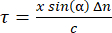 , with c speed of light, α apex angle of the wedges, Δn= ne-no difference in ordinary and extraordinary refractive indexes (birefringence). Since the spectral resolution Δv is inversely proportional to the scan range T=|T2-T1|, with T1, T2 initial and final delay of the interferogram, the high spectral resolution required by Raman spectroscopy calls for high birefringence and long wedge translations. Among the most common birefringent crystals, YVO4 (yttrium orthovanadate) is particularly suited for its high Δn and transparency range in the visible-near infrared. The wedges are designed with an apex angle of 10°, thus, with a scan length of 15.3 mm, the interferometer can impart a delay of 2500 fs at 600 nm, obtaining a spectral resolution of 23 cm-1, over the entire spectral range of interest (the silicon camera sensitivity poses the upper limit). This work will present the strategy for a proper setting of the interferogram sampling (i.e., step and scan range) to achieve the desired spectral resolution and to deal with the broadband background, disentangling the Raman signal from photoluminescence.
As described by Candeo et al.17, this birefringent spectrometer can be coupled with a commercial optical microscope to perform hyperspectral measurements. The requirements are the following: a reconfigurable optical microscope body, a TWINS birefringent interferometer, a low-noise monochrome camera (e.g., CCD or sCMOS), and a narrowband laser source. For the latter, typical excitation wavelengths for Raman and fluorescence spectroscopy are 355 nm, 488 nm, 514 nm, 532 nm, 633 nm, and 785 nm. Despite high-spectral purity lasers, such as the one listed in the Table of Materials, being the best choice, a laser with a broader line width, e.g., ~0.1 nm, can be used as well, given the limited spectral resolution of the instrument. The microscope is upgraded by placing the TWINS in the detection path, between the tube lens and the monochrome detector. This configuration provides a uniform path delay across the field of view and an average contrast of 55%. The excitation path is designed to get a uniform illumination of the sample: in practice, the output tip of a large-core multimode fiber is imaged on the sample plane. By using a mechanical scrambler, the modes are strongly coupled in the core of the fiber, producing a flat-top profile on the sample plane. In addition, a vibrating voice coil averages out the speckle pattern typical of monochromatic radiation. A characterisation of this top-hat illumination is shown in Supplementary Figure 1. The beam is focused on the sample by an infinity-corrected objective, which also collects backscattered Raman and luminescence light toward the detection path. The filters required to reject illumination will be detailed.
To show how to measure broadband and narrowband spectral features with this hyperspectral microscope, both luminescence and Raman scattering are measured for a test sample specifically selected for illustrative purposes. The sample consists of a mixture of three powder pigments with well-known Raman spectra: two polymorphs of titanium white (TiO2), namely rutile and anatase, and cadmium sulphide yellow (CdS). However, the same procedure can be used for a broader range of applications, from materials science to biology.
The scope of this article is to illustrate the steps to perform a hyperspectral measurement, while the assembling and alignment of the TWINS interferometer are detailed by Candeo et al.17. Therefore, an interested experimenter should start from a pre-assembled interferometer based on this technology.
The protocol starts with the sample preparation and how to set up the microscope to excite and collect the Raman scattering and PL photons. Then, the scan parameters (scan length, sampling step) and acquisition parameters (exposure time, hardware binning) are set according to the requirements of the signal under investigation. Finally, the post-processing pipeline will be presented, detailing the procedure for retrieving the spectrum at each pixel (spectral hypercube, Figure 2B) from the acquired temporal dataset (temporal hypercube, Figure 2A), and outlining the algorithms for noise reduction and advanced spectral analysis. The entire workflow is shown in Figure 3.
Access restricted. Please log in or start a trial to view this content.
Protocol
The reagents and the equipment used in this study are listed in the Table of Materials.
1. Sample preparation
CAUTION: Wear latex gloves during this preparation since CdS pigment is toxic, especially when it is inhaled.
- Use a scraper to deposit 20 mg of each pigment powder on a precision balance, obtaining a 1:1:1 weight proportion.
NOTE: Carefully clean the scraper tip for each sample to avoid cross-contamination. - Mix the powders with a mortar to remove clumps.
- Pour the resulting mixture onto a microscope slide; use the scraper tip to gently press it and obtain an almost uniform thickness of the layer.
- Apply nail polish on the edges of a microscope coverslip. Place it on the mixture, with the nail polish facing down, and apply enough pressure to seal it. Let it dry for a few seconds to harden the polish.
2. Microscope set up
CAUTION: Wear safety glasses when the laser is on, since the maximum power achievable on the sample plane is 300 mW.
NOTE: Pump laser performance remains unaffected by temperature variations, as long as it is operated within the temperature range specified in the datasheet (e.g., 10-40 °C for the laser reported in the Table of Materials).
- Align the TWINS interferometer along the detection path of the microscope.
NOTE: As detailed by Candeo et al.17, the interferometer module must be added between the tube lens and the detector, ensuring a proper distance between them. For the microscope used in this work, this is guaranteed only when the eyepiece module is removed. - To adapt the Koehler illumination scheme to a laser excitation, remove the built-in excitation lamp of the microscope and use a microscope objective to collect the light at the output of a large-core multimode fiber.
NOTE: The objective magnification sets the size of the illumination pattern when the tip of the fiber is conjugated with the sample plane. A possible choice is a 10x/0.25-0.30 objective. - Choose the excitation wavelength and focus the excitation laser at the input of the large-core multimode fiber. Switch on the camera and run a visualisation software.
- Attach a middle section of the fiber to the vibrating membrane of a voice coil, which will remove the speckle. Mechanically scramble the fiber by tightly bending it to merge all its spatial modes. Switch on the laser.
- Prepare a test sample for alignment, e.g., fluorescent red marker stripes on a microscope coverslip.
- Adjust the position of the fiber tip with respect to the illumination optical system by moving the fiber with a precision translation stage to get a spot with uniform intensity and well-defined edges on the sample plane.
NOTE: A 532-nm laser is used for all the reported measurements. With a 400-µm-core-size fiber, the diameter of the spot covers 82% of the camera FOV width.
- Employ a filter set for the excitation and detection paths, adopting the following criteria (Supplementary Figure 2):
- Use a narrow bandpass filter at 532 nm (2.0-nm bandwidth) to clean the laser line and reject any pump sidebands arising from nonlinear broadening due to propagation in the fiber.
- Use a dichroic mirror (DM in Figure 1) to reflect the laser light toward the sample and transmit the redshifted backscattered radiation collected by the objective.
- Use a long-pass filter (LPF in Figure 1) at 532 nm to reject residual illumination light.
- During Raman scattering measurement, use a short-pass filter (SPF in Figure 1) at 600 nm to suppress background fluorescence.
- Measure the power on the sample plane with a power meter. Attenuate the pump beam to obtain an intensity at the sample which does not lead to damage (of the order of 2 W/cm2, as reported in Table 1). Use a shutter for the laser while setting the other measurement parameters.
NOTE: Due to the low cross-section of spontaneous Raman scattering, high power density is needed to enhance signal collection. However, the sample damage threshold must be considered. Unlike point-scanning systems, a wide-field setup illuminates a large area, making power dissipation less efficient and requiring careful power management to prevent sample damage. - Put the sample on the microscope stage and adjust the focus.
NOTE: To find the focus easily, first illuminate the sample with a white lamp in transmission or reflection. In the latter case, a light bulb placed beside the microscope could be used.The sample focus will be subsequently optimised with the pump laser light.
3. Measurement parameters
- Switch on the driver of the motor that performs the wedge translation. Control the hardware components (camera and motor) simultaneously to perform hyperspectral measurements (example of user interface shown in Supplementary Figure 3).
- Set the camera acquisition parameters, exposure time, and hardware binning to optimise the signal intensity, adopting the following instructions:
- Since a high signal-to-noise ratio (SNR) in the temporal signal leads to a high SNR in the retrieved spectra, privilege a long exposure time, which better fills the sensor dynamic range.
NOTE: For low signals, as for Raman scattering, one must find a compromise between signal level and total measurement time: the longest exposure time may not be feasible. - Choose hardware binning to collect charge from more pixels before readout.
NOTE: Summing charge and doing a single readout gives better noise performance than reading out several pixels and then summing their signal in post-processing. The choice of binning is also driven by the acceptable reduction of spatial resolution.
- Since a high signal-to-noise ratio (SNR) in the temporal signal leads to a high SNR in the retrieved spectra, privilege a long exposure time, which better fills the sensor dynamic range.
- Choose scan parameters, total scan length, and sampling step according to the following criteria:
- To achieve a high spectral resolution for Raman peaks, set an asymmetric long wedge translation (-2526 fs→ -36 fs). On the other hand, perform a symmetric scan around the zero delay position (-65 fs → 65 fs) to retrieve more broadband spectral features of the PL signal.
- Using Equation 1 for delay τ as a function of wedge translation x, choose the sampling step to fulfil the Nyquist limit for the spectral bandwidth of interest.
NOTE: Given the minimum wavelength of the spectrum λmin, impose (Equation 2).
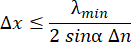
where the birefringence Δn is wavelength-dependent (see Sellemeier's equations).
- Open the shutter to shine the laser on the sample. If a decrease in signal intensity is observed, wait till the sample has reached a stationary condition (typically a few seconds).
NOTE: To compensate for the decrease in signal intensity, adjust binning and exposure time to maintain a good SNR. - Start the acquisition of a monochrome image for each wedge position, i.e., temporal delay between replicas from each point of the 2D sensor.
NOTE: The acquisition software should save two variables: the temporal hypercube (2D image set) and the vector of motor positions recorded by the encoder during the scan. - Once the measurement is finished, switch off the laser and proceed with the data analysis.
4. Processing of the acquired datacube
- Generate the spectral hypercube from the acquired dataset, following these instructions:
- Load the motor positions correction file for the specific stepper motor (see the discussion).
- Load the frequency calibration file for the specific interferometer to associate measured spatial frequencies (pseudofrequencies) with real optical frequencies (see the Discussion section).
- Choose the frequency range for the spectra that will be computed by Fourier transforming the interferograms of all pixels.
- Among the available apodization functions12 for windowing the measured interferogram, select the one that offers a good trade-off between spectral broadening and artefact reduction in the retrieved spectra, such as the Happ-Genzel (Hamming) window.
- Generate the spectral hypercube by Fourier transforming the apodized interferograms for all pixels. Save it in complex values.
NOTE: The complex spectrum from FT carries additional information, which will be useful to denoise the dataset and extract the average spectra of a set of selected pixels.
- Once the spectral hypercube has been computed, perform various investigations, e.g, obtain the average spectrum in selected areas; generate a false-colour RGB image; map spectral peaks; subtract background.
- To reduce spectral noise, which may overwhelm significant peaks, especially in Raman spectra, implement the Singular Value Decomposition (SVD)18 by following these steps:
- Reshape the temporal hypercube into a matrix A with interferograms along its rows.
- Perform the SVD of the matrix, obtaining U, S, and V matrices such that A = USVT.
NOTE: U columns are the spatial distributions of the eigenvectors of V (columns), while S is a diagonal matrix with singular values (SVs) in descending order. - Reshape each column of U into a matrix of pixels and perform its 2D FT to obtain its spatial frequencies.
- Since high frequencies are associated with very abrupt changes in the map, consider them as noise; define a square region centred in the computed Fourier space that separates low (mainly signal) and high (mainly noise) frequencies.
NOTE: A possible choice for this area is with a side of ¼ with respect to the Fourier space size. - Compute the spatial signal ratio (SSR) for each SV by dividing the sum of pixel intensities (complex modulus) within the boundary by the sum of intensities outside the boundary. Plot SSR as a function of SV number.
- Define a threshold for SSR, i.e., the number of significant SVs to keep in order to reduce noise contribution in the dataset, avoiding artefacts.
NOTE: SSR typically shows a decreasing trend that levels off into a plateau as the number of singular values increases. A rule of thumb is to retain singular values up to the point where the plateau begins. - Set all the lower SVs to zero in the diagonal matrix S, obtaining Sdenoised, and compute a denoised temporal hypercube as USdenoised VT.
NOTE: SVD is a matrix factorisation that can also be applied to the reshaped spectral hypercube (with rows containing spectra rather than interferograms).
- Repeat steps 4.1-4.2 with the denoised temporal hypercube to retrieve the spectra.
- Download the program from the link in Reference19 to perform a deeper analysis of the dataset with the Multivariate Curve Resolution-Alternating Least Squares (MCR-ALS) algorithm.
NOTE: Software developers provide a detailed description of the algorithm20. It is an iterative method to solve the mixture analysis problem: each spectrum is expressed as the linear combination of pure spectral profiles. With a matrix representation: B = C RT+E, where B is the dataset, C contains the concentrations for each spectrum, columns of R are the reference spectra of the constituents, and E expresses the error.- Reshape the spectral hypercube into an Npix x Nfreq matrix, with Npix total number of pixels and Nfreq frequency vector length.
- Select the number of species expected in the sample and load their reference spectra.
NOTE: Reference spectra can be measured for each pigment separately. Otherwise, the program will make an SVD of the dataset and use as many principal components as the selected constituents for initial guesses. - Select constraints: retrieved spectral profiles must be non-negative and as similar as possible to reference spectra.
- Plot the concentration map (reshaped columns of C) and spectra (columns of R) for each species.
- Export these maps and use them to produce a false-colour image (Figure 4A), concluding the analysis.
NOTE: The programmes used to obtain the results presented here are not publicly available, but may be obtained from the authors upon request.
Access restricted. Please log in or start a trial to view this content.
Results
Figure 4A shows the Raman map for a selected region of the powder mixture. It is a false-colour representation of the abundance maps retrieved with MCR-ALS, as described in step 4.5. It provides information about the sample composition, since the three species can be clearly distinguished within the FOV. Figure 4B shows the average spectra in the selected regions of the map, with a spectral resolution of 23 cm-1 defined by the chosen scan length. The ...
Access restricted. Please log in or start a trial to view this content.
Discussion
A wide-field FT multimodal microscope has been introduced for the acquisition of spontaneous Raman scattering and luminescence images, and it is applicable to materials science. The applicability to biological samples is demonstrated by Candeo et al.17, who presents a hyperspectral fluorescence image of stained human cells. The main challenge for Raman scattering measurements in this field is to prevent photodamage resulting from inefficient heat dissipation from a widely illuminated area. A ...
Access restricted. Please log in or start a trial to view this content.
Disclosures
The authors declare no conflicts of interest.
Acknowledgements
G.C. acknowledges support by the European Union Marie Skłodowska-Curie Actions project ENOSIS H2020-MSCA-IF-2020-101029644 and by the European Union's Horizon Europe (HORIZON) research and innovation programme under the Marie Skłodowska-Curie Action PIONEER (Grant Agreement 101066108). G.V. and G.C. acknowledge support by the European Union's NextGenerationEU Programme with the IPHOQS Infrastructure [IR0000016, ID D2B8D520, CUP B53C22001750006] "Integrated Infrastructure Initiative in Photonic and Quantum Sciences".
Access restricted. Please log in or start a trial to view this content.
Materials
| Name | Company | Catalog Number | Comments |
|---|---|---|---|
| Anatase | Kronos | 1200 | Polymorph of White TiO2 pigment |
| Cadmium sulfide powder | Kremer Pigmente GmbH & Co. | 21060 | Cadmium yellow, colour index dark/PY35 |
| Camera | Andor | Luca R | Electron multiplying CCD camera with 1004x1002 pixels of 8µm x 8µm |
| Clean-up filter | Semrock | LL01-532-12.5 | Ø1/2" 2.0 nm- FWHM laser-line filter at 532 nm |
| Coverslips | BRAND GmbH & Co | 4700 55 | Borosilicate glass 22x22x0.15 mm microscope coverslips |
| Dichroic mirror | Semrock | Di02-R532-25x36 | 25.2x35.6 mm single-edge laser dichroic beamsplitter at 532 nm |
| Fiber | Thorlabs | M74L05 | 400µm-core size, NA 0.39 multimode fiber |
| Laser | Hubner Photonics | Cobolt Samba 1000 | CW diode pumped laser at 532 nm, maximum power 1000 mW |
| Long pass filter | Semrock | LP03-532RU-25 | Ultra steep long-pass edge filter at 532 nm |
| Microscope | Leica | DMRBE | Trinocular research microscope |
| Objective | Leica | PL-FLUOTAR, 10x/0.30 | Excitation and collection objective with 10x magnification, 0.3 NA |
| Objective | Newport | M-10X | Objective lens in illumination path, with 10x magnification, 0.25 NA |
| Rutile | Kronos | 2900 | Polymorph of White TiO2 pigment |
| Short pass filter | Thorlabs | FESH600 | Ø25.0 mm shortpass filter with cut-off wavelength 600 |
| Slides | Marienfeld | 1000612 | 76x26x1 mm microscope slides |
References
- Dicker, D. T., Lerner, J. M., El-Deiry, W. S. Hyperspectral image analysis of live cells in various cell cycle stages. Cell Cycle. 6 (20), 2563-2570 (2007).
- Sellar, R. G., Boreman, G. D. Classification of imaging spectrometers for remote sensing applications. Opt Eng. 44 (1), 013602-013602 (2005).
- McCreery, R. L. Raman spectroscopy for chemical analysis. , 1st Edition, John Wiley & Sons. (2000).
- Vanna, R., et al. Vibrational imaging for label-free cancer diagnosis and classification. La Rivista del Nuovo Cimento. 45 (2), 107-187 (2022).
- Zhang, S., et al. Spotting the differences in two-dimensional materials-the Raman scattering perspective. Chem Soc Rev. 47 (9), 3217-3240 (2018).
- Wang, Y., et al. Multi-point scanning confocal Raman spectroscopy for accurate identification of microorganisms at the single-cell level. Talanta. 254, 124112(2023).
- Qin, J., et al. Line-scan Raman imaging and spectroscopy platform for surface and subsurface evaluation of food safety and quality. J Food Engg. 198, 17-27 (2017).
- Hagen, N., Kudenov, M. W. Review of snapshot spectral imaging technologies. Opt Engg. 52 (9), 090901-090901 (2013).
- Morris, H. R., Hoyt, C. C., Treado, P. J. Imaging spectrometers for fluorescence and Raman microscopy: Acousto-optic and liquid crystal tunable filters. Appl Spectr. 48 (7), 857-866 (1994).
- Wiener, N. Generalized harmonic analysis. Acta Mathematica. 55 (1), 117-258 (1930).
- Bell, R. Introductory Fourier transform spectroscopy. , 1st Edition, Elsevier. (1972).
- Griffiths, P. R. Fourier Transform Infrared Spectrometry. , 2nd Edition, John Wiley & Sons. (2007).
- Jullien, A., Pascal, R., Bortolozzo, U., Forget, N., Residori, S. High-resolution hyperspectral imaging with cascaded liquid crystal cells. Optica. 4 (4), 400-405 (2017).
- Müller, W., Kielhorn, M., Schmitt, M., Popp, J., Heintzmann, R. Light sheet Raman micro-spectroscopy. Optica. 3 (4), 452-457 (2016).
- Wadduwage, D. N., et al. Near-common-path interferometer for imaging Fourier-transform spectroscopy in wide-field microscopy. Optica. 4 (5), 546-556 (2017).
- Brida, D., Manzoni, C., Cerullo, G. Phase-locked pulses for two-dimensional spectroscopy by a birefringent delay line. Opt Lett. 37, 3027-3029 (2012).
- Candeo, A., et al. A hyperspectral microscope based on an ultrastable common-path interferometer. APL Photonics. 4 (12), 120802(2019).
- Camp, C. H. Jr, Lee, Y. J., Cicerone, M. T. Quantitative, comparable coherent anti-Stokes Raman scattering (CARS) spectroscopy: correcting errors in phase retrieval. J Raman Spectr. 47 (4), 408-415 (2016).
- Multivariate curve resolution homepage. , Available from: https://mcrals.wordpress.com/download/mcr-als-2-0-toolbox/ (2021).
- de Juan, A., Jaumot, J., Tauler, R. Multivariate Curve Resolution (MCR). Solving the mixture analysis problem. Anal Methods. 6 (14), 4964-4976 (2014).
- Di Benedetto, A., Pozzi, P., Valentini, G., Comelli, D. Integrating multimodal Raman and photoluminescence microscopy with enhanced insights through multivariate analysis. J Phys: Photonics. 6 (3), 035019(2024).
- Rosi, F., et al. UV-Vis-NIR and micro Raman spectroscopies for the non-destructive identification of Cd1-xZnxS solid solutions in cadmium yellow pigments. Microchemical J. 124, 856-867 (2016).
- Ghirardello, M., Kelly, N. M., Valentini, G., Toniolo, L., Comelli, D. Photoluminescence excited at variable fluences: A novel approach for studying the emission from crystalline pigments in paints. Anal Methods. 12 (32), 4007-4014 (2020).
- Ardini, B., et al. High-throughput multimodal wide-field Fourier-transform Raman microscope. Optica. 10 (6), 663-670 (2023).
- Pickett, H. M., Strauss, H. L. Signal-to-noise ratio in Fourier transform spectrometry. Anal Chem. 44 (2), 265-270 (1972).
Access restricted. Please log in or start a trial to view this content.
Reprints and Permissions
