This article traces the life cycle of a silicon nitride membrane resonator, from design through fabrication to characterization.
A subscription to JoVE is required to view this content. Sign in or start your free trial.
Method Article
Fabrication and Characterization of High-Q Silicon Nitride Membrane Resonators
In This Article
Summary
Abstract
Silicon nitride membranes are a widely used optomechanical resonator platform, offering high mechanical Q, low optical loss, and enhanced optomechanical coupling using a panoply of strain, phononic-crystal, and photonic-crystal engineering techniques. Despite their ubiquity, fabrication and characterization of silicon nitride membranes often rely on tacit knowledge shared between research groups. This article presents a detailed video walk-through of the design, fabrication, and characterization of a contemporary silicon nitride membrane resonator (specifically, a centimeter-scale Si3N4 nanoribbon supporting torsional modes with Q-factors exceeding 108 at room temperature). The protocol covers finite element simulation, wafer- and chip-scale processing, and optical lever-based readout. Special attention is given to photolithographic patterning, dry- and wet-etching, device handling, and ringdown measurement. The tutorial is intended as both a practical entry point for newcomers and a reference for experienced groups replicating or adapting similar devices. All procedures are demonstrated in standard university cleanroom and benchtop environments.
Introduction
Silicon nitride membranes have played an important role in quantum optomechanics1 over the last two decades, beginning with the discovery that a commercial membrane (a TEM slide) can support drum modes with Q-frequency products exceeding 1013 Hz and be coupled to a high finesse optical cavity using the membrane-in-the-middle approach2,3,4. Gradually it was appreciated how tensile stress and mode shape affect the mechanical Q (through an effect called dissipation dilution5,6), spurring the invention of micropatterned membranes—trampoline7,8, 2D an1D phononic crystal9,10, fractal11, and perimeter mode resonators12—with Q factors as high as 109. In conjunction with cryogenics, these devices have enabled landmark experiments such as ground state cooling13,14, ponderomotive squeezing15, optomechanical entanglement16, and displacement measurement beyond the Standard Quantum Limit17,18. They also feature prominently in proposals for next generation optomechanical technologies and probes for new physics, including membrane-based force microscopes19, accelerometers20, spectroscopes21, quantum memories22, microwave-to-optical photon transducers23, and dark matter detectors24.
Despite their popularity, the design, fabrication, and characterization of silicon nitride membrane resonators remain a niche discipline within the optomechanics community, relying on bespoke techniques handed down by word of mouth and dissertations25,26,27,28,29,30,31,32. A recent review of interferometric characterization of nanomechanical resonators demystifies the latter task33, and modeling of dissipation dilution has become simple with commercial finite element simulation software28. Nanofabrication, however, remains an obstacle to entry, since the procedure, while straightforward, involves a sequence of delicate steps whose nuances are often left out of traditional verbal descriptions and process flow diagrams.
This article presents the design, fabrication, and characterization of a silicon nitride membrane resonator in video format, using a centimeter-scale nanoribbon34—a simple yet robust platform gaining popularity for torsional quantum optomechanics35,36 and precision measurement37,38—as an example (the procedure is readily adaptable to other resonator geometries). The design segment provides a basic overview of simulating membrane modes using commercial finite-element software. The fabrication sequence, which forms the core of the tutorial, covers substrate preparation, film deposition, patterning, etching, and release. The article concludes with a demonstration of characterization using the optical lever (OL) technique. This resource is intended as a practical starting point or refresher for researchers working with high-Q membrane resonators.
Access restricted. Please log in or start a trial to view this content.
Protocol
1. Simulation and design 32,28
- Choose resonator parameters to optimally fit a predetermined objective
- Build a COMSOL model of the generic resonator geometry of interest. Start the software model wizard and create a 2D simulation. Under the structural mechanics physics menu, select either Plate or Shell.
NOTE: The difference between plate and shell is minimal in this context. - For the purposes of design, the device's frequency, mode shape, effective mass, and quality factor are of highest interest. So, select Eigenfrequency, Prestressed in the Select Study menu.
- Construct the resonator geometry and set the material of all domains to stoichiometric silicon nitride (Listed as Si3N4- silicon nitride in the software material library).
NOTE: The mechanical properties of silicon nitride vary depending on stoichiometry and deposition process. We alter the default material density to 2700 kg/m3 to reflect the films used in this work (see below). - Add an initial stress and strain to the model corresponding to the prestress of the Si3N4 film (In this case, we specify 1 GPa). Then add a fixed constraint node and select the Device's clamps.
- Under the Mesh node, choose the Extremely Fine element size option. Choosing this option is important for accurate dissipation dilution simulation. To further increase accuracy, scale the mesh density in the Mesh Density window.
- Go to the stationary study step and ensure that the Include geometric nonlinearity box is checked. Under the eigenfrequency study step, choose how many modes to solve for and run the simulation.
- Under the results node, add a global evaluation that estimates the resonator's quality factor arising from dissipation dilution-the ratio of the total kinetic and elastic strain energy times the intrinsic quality factor28,32,39.
- Modify the resonator's geometry until the effective mass, frequency, and quality factor meet specifications.
- Transfer the design geometries to a GDSII CAD file and populate a wafer CAD (for this work, we use positive photoresist so only the area around the resonator is modeled).
- In addition to a layer of resonators, add a bottom layer representing back windows on each device to remove material from behind each device. Doing so also hastens the wet etch process later in the protocol.
- Finally, place dice lines and four alignment markers on the top, bottom, and sides of the wafer CAD on both layers. This helps properly align the wafer backside when running the photolithography machine.
- Build a COMSOL model of the generic resonator geometry of interest. Start the software model wizard and create a 2D simulation. Under the structural mechanics physics menu, select either Plate or Shell.
2. Wafer-scale fabrication 1
NOTE: Si3N4 deposition can be performed by the reader, but our facilities lack the necessary equipment to do so, and, as such, we start with commercially sourced wafers for this study. An overview of the fabrication process is shown below in Figure 1.
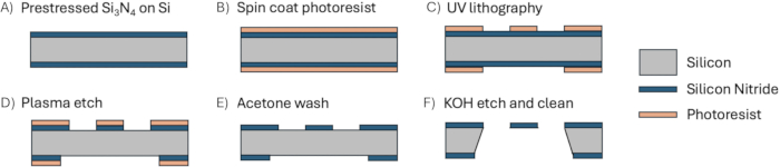
Figure 1: Fabrication overview. (A) A thin film of silicon nitride is deposited onto a bare silicon substrate. The wafer is then (B) coated with photoresist for (C) photolithography. The pattern traced out in (C) is used as a protective mask for (D) reactive ion etching to carve the resonator designs into the film. After dicing, (E) acetone is used to remove the resist before (F) potassium hydroxide solution removes the silicon substrate. Please click here to view a larger version of this figure.
- Pattern the design(s) found in the previous section onto a double-sided Si3N4-on-Si wafer. Deposit a high-stress thin film of Si3N4 onto a bare silicon substrate using low-pressure chemical vapor deposition (LPCVD). Typical deposition parameters are: Quartz temperature = 800 °C, Pressure = 10 mTorr, Injected gas mixture = Dichlorosilane (SiH2Cl2) and ammonia (NH3)
CAUTION: SiH2Cl2 is combustible and corrosive. It is acutely poisonous if inhaled and should only be handled with extreme care and proper personal protective equipment (PPE). NOTE: We outsource to a third-party wafer processing for this step, as is customary. - Hexamethyldisilazane (HMDS) vapor-phase priming40
NOTE: The following steps can be replaced if one has access to an HMDS oven, which automates the priming process.- Place a clean, double-sided Si3N4-on-Si wafer on two glass slides inside a wide glass Petri dish. Space the slides such that only the outer edge of the wafer is supported, improving the backside priming in later steps.
- Place a few drops of HMDS along the edge of the Petri dish with a disposable capillary pipette. Under a fume hood, cover the glass Petri dish and heat to 90 °C for 1 min on a hot plate, evaporating the HMDS and allowing it to adhere to the Si3N4.
CAUTION: HMDS is combustible, irritant, and causes long-term health problems if inhaled and should only be handled under a fume hood. - After 1 min, remove the petri dish cover gently and vent any remaining HMDS from the dish. Move the wafer to a plastic Petri dish with a cleanroom wipe on the bottom.
- Spin coating resist
- Before depositing resist, preheat a hotplate to 115 °C. This will ensure the hotplate is at the prescribed temperature later in the protocol.
- Center the primed wafer inside a spin coater and hold in place with a vacuum chuck. Leave the spin coater open for later steps.
- Using a needle and syringe, extract no more than 4 mL of S1813 photoresist41. Gently flick the syringe and dispense a small amount of fluid to remove air bubbles.
CAUTION: S1813 is a combustible irritant and should only be handled with proper PPE and away from open flames or sparks. - Holster the needle and replace with a 2 µm filter to remove large particulates. As in the previous step, gently flick the syringe and dispense 3-5 drops of fluid to remove remaining air bubbles in the filter. Before continuing, make sure at least 3 mL of resist remains in the syringe.
- Deposit the resist drop by drop onto the wafer to form one large pool. As this pool gets larger, deposit the resist near its edge to ensure it stays relatively centered on the wafer. If any bubbles appear on the pool surface, use the needle tip to pop them before continuing.
- Lock the spin coater lid and set to spin at 3000 rpm for 30 s with an acceleration of 3000 rpm/s. These settings, according to the resist manufacturer, will create a uniform 1.5 µm thick layer across the wafer surface6.
- Inspect the finished coat for bubbles, streaks, and non-uniformity. If any are spotted, shut the spin coater and wash the wafer surface with acetone and isopropyl alcohol (IPA). Running the spin coater during this step enhances the removal.
- Repeat steps 2.3.1-2.3.7, to form a new layer.
CAUTION: Acetone and IPA are both combustible irritants. They should only be handled with proper PPE and away from open flames or sparks. - If the resist layer is defect-free, disable the vacuum chuck and transfer the wafer to the preheated hot plate for a 1 min bake6. Baking the wafer evaporates leftover solvent and prepares it for photolithography.
- After baking, remove the wafer from the hotplate. Proceed to the photolithography step.
- Photolithography
- Load the coated wafer into a maskless alignment (MLA) photolithography machine. Make sure to center the wafer as best as it can to minimize global rotation and offset errors.
- Load the populated wafer file from step 1.2 onto the computer and convert to a file type which can be understood by the MLA software. Begin by patterning the topside layer populated with resonator designs.
- After loading the wafer and CAD file, select the corresponding wafer shape and size. The machine automatically determines alignment by using an edge-detection algorithm.
- After alignment, select the option to include global rotation error and load the following beam exposure parameters. Beam intensity of 140 mJ/cm2 at a wavelength of 375 nm produces optimal results for 1.5 µm of this resist1.
- With all exposure parameters loaded and the wafer aligned, begin the exposure. For a 100 mm wafer divided into 12 mm square chips, this process usually takes about 20 min.
- At 5 min before the end of the photolithography exposure, rinse two large dishes with deionized (DI) water and blow dry with compressed nitrogen gas.
- Fill one dish with about 75 mL of MF-319 developer42and the other with a large amount of DI water.
CAUTION: MF-319 is corrosive, irritating, and poses long-term health risks. Only use with proper PPE. - Once the exposure is complete, unload the wafer from the MLA and transfer to the MF-319 developer to be left undisturbed for 20 s.
- After 20 s of development, agitate the solution to remove exposed resist for an additional 40 s by gently swirling the dish in a circular motion. If exposed resist remains, agitate the mixture for an additional 30 s, but take caution not to overexpose the wafer42.
- Transfer the wafer to the second dish filled with DI water to dilute off residual developer. Gently wash with DI water using either a wash bottle or a DI water gun on both sides to remove the rest.
- Finally, point a compressed nitrogen gas gun along the wafer to remove the DI water from the wafer surface. Use low pressure and proper gun orientation to minimize the chance of damage.
- Reactive ion etch40
- Load the developed wafer into a reactive ion etcher to transfer the resist patterns onto the Si3N4 film. Run the following process for 5 s at a time, removing 30 nm of Si3N4 [40]; Gas composition: 30 sccm of sulfur hexafluoride (SF6) and 10 sccm of Argon (Ar); High frequency bias: 50W; Power of inductively coupled plasma: 1000 W; Chamber pressure: 10 mTorr.
NOTE: Since sidewall profiles are negligible, this etch can be continuous instead of stepped. A stepped process, however, reduces the risk of hard-baking the resist. - Repeatedly run this process to remove about 30 nm of Si3N4 per process until the exposed film appears silver, an indicator that the substrate is exposed. Finally, remove the wafer from the reactive ion etcher; the wafer is now ready for backside patterning.
- Load the developed wafer into a reactive ion etcher to transfer the resist patterns onto the Si3N4 film. Run the following process for 5 s at a time, removing 30 nm of Si3N4 [40]; Gas composition: 30 sccm of sulfur hexafluoride (SF6) and 10 sccm of Argon (Ar); High frequency bias: 50W; Power of inductively coupled plasma: 1000 W; Chamber pressure: 10 mTorr.
- Backside patterning
- Place the wafer back into the spin coater with the device side facing down. Deposit a 1.5 µm layer of photoresist identical to step 2.3.
NOTE: Since the resist layer from step 2.4 survives the plasma etch in step 2.5, it acts as a protective layer that prevents damage to the film underneath. - With the new resist layer facing up, load the wafer back into the MLA, rotate 180°. Reload the wafer CAD into the MLA software, convert to an acceptable file type, and mirror along the respective axis. Viewing the converted CAD ensures that the CAD orientation matches that of the wafer.
- Repeat steps 2.4.3-2.5.2.
- Place the wafer back into the spin coater with the device side facing down. Deposit a 1.5 µm layer of photoresist identical to step 2.3.
- Wafer cleaving
- Using the dice lines patterned into silicon nitride as a guide, place two glass slides on the wafer such that they are parallel to the substrate crystal plane. Carefully insert a diamond-tipped scribe between the slides and drag along the dice lines, scoring along the crystal plane.
- Re-align the slides to a new dice line and use the scribe to score along another part of the wafer. Repeat this scoring process until all edges of individual chips have been scribed.
- Place the wafer on top of the slides such that a dice line is equidistant from both. If the score was deep enough and well aligned, a small amount of force to the top of the wafer is enough to cleave the wafer along the crystal plane, resulting in a perfect break. Break the pieces of the wafer continuously in this fashion to make individual chips.
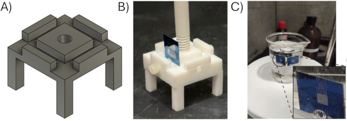
Figure 2: Custom chip holder. The custom chip holder is designed to keep chips upright while maximizing exposed area for KOH etching. (A) CAD drawing showing the basic structure of the device. The final structure is machined out of a small block of PTFE Teflon for chemical resistance. (B, C) Chips are placed upright in the holder, and a PTFE stick is used to lower them into a chemical bath. This figure has been modified from32. Please click here to view a larger version of this figure.
3. Chip-scale processing 32
- Release the patterned resonators from their silicon substrate to produce free-standing films.
- First, add 40 mL of 45% concentration potassium hydroxide (KOH) solution to a vessel (or beaker) and heat to 86 °C using a hotplate. Cover the solution to promote a uniform temperature gradient.
CAUTION: KOH is corrosive and an irritant and should only be handled with proper PPE under a fume hood. - Remove dust from a plastic sample holder (with a lid) using a strong puff of nitrogen gas and rinse a thin metal washer the size of the chip with IPA and blow dry with compressed nitrogen gas. The washer will act as a stand for the released membrane inside this holder.
- Peel diced chips carefully from their tape and dip in a sonicated acetone bath for at least 30 s to remove resist and surface contaminants. Wash off the acetone with a quick IPA rinse and dry with compressed nitrogen gas.
- OPTIONAL: To thin the Si3N4 film and/or to remove stuck-on contaminants, dip the chip in a 10% hydrofluoric acid (HF) buffer solution to remove 1.55 nm/min. This step is optional in that it can be performed before or after the KOH etch.
CAUTION: HF is acutely poisonous, corrosive, and requires specific safety considerations before being used. Only handle with proper training, acid-safe gloves/aprons, and with calcium gluconate gel ready in case of exposure. - To prevent foreign contaminants from reattaching to the chip, place it immediately in a custom polytetrafluoroethylene (PTFE) holder1 under a fume hood. This holder is shown in Figure 2.
- First, add 40 mL of 45% concentration potassium hydroxide (KOH) solution to a vessel (or beaker) and heat to 86 °C using a hotplate. Cover the solution to promote a uniform temperature gradient.
- KOH wet etch
- Lower the custom chip holder into the KOH bath. Cover the solution to maintain a uniform thermal gradient. Since KOH etches silicon at a rate of about 10 µm/hr for a bath temperature of ~62 °C and concentration of 45%43,44 (about one day of etching for a 200 µm thick wafer, depending on the device geometry), set up a camera next to the etch for long-distance monitoring.
NOTE: The KOH reacts with silicon preferentially along the crystal plane of the substrate. While the etch rate along with other directions is small, it remains nonnegligible, etching corner features slowly2. - After all silicon around the resonator has been etched and the film is released, stop the reaction by removing the vessel from the hot plate. Due to the viscosity of KOH, removing the device would likely shatter the film8, so replace the KOH bath gradually with DI water by iteratively pipetting out KOH and pipetting in DI water, never letting the liquid level fall below the top of the chip. Repeat this process until all the vessel volume has been removed.
- To prevent cross-contamination with KOH and solvents later in this protocol, transfer the chip holder to a fresh DI water bath.
- Fill a large vat with excess DI water, enough to cover both the etching and DI vessels with room for the holder above. Place the new DI water bath in the vat using tongs, followed by the etching vessel.
- Use the dip stick to gently lift the chip holder out of the etching vessel and, while keeping the chip submerged, transfer to the DI bath. Remove both vessels from the vat with tongs, leaving the chip holder in a clean DI water bath.
- Lower the custom chip holder into the KOH bath. Cover the solution to maintain a uniform thermal gradient. Since KOH etches silicon at a rate of about 10 µm/hr for a bath temperature of ~62 °C and concentration of 45%43,44 (about one day of etching for a 200 µm thick wafer, depending on the device geometry), set up a camera next to the etch for long-distance monitoring.
- Cleaning the released film
- After the chip has been transferred to a fresh DI water bath, replace the DI water gradually with IPA in the same fashion as step 3.2.2. Again, never let the liquid level fall below the top edge of the chip.
- After two baths' worth of liquid has been transferred out, repeat the process, replacing IPA with methanol.
- After two baths' worth of liquid have been transferred out, remove the device from the methanol bath and carefully blow dry along the chip plane with a gentle current of nitrogen gas.
NOTE: The released film is extremely delicate and must be handled with care. To minimize the chance of breaking or contaminating the film, the device should be held by the chip edge or corner using carbon fiber-tipped forceps. When handling in a liquid bath, the chip should be moved out of the plane of the film, such that the fluid just grazes the surface. - Inspect the device under a microscope for debris, leftover resist, or flaws. Clean as necessary by placing the chip back in methanol for some time and re-drying.
- HF wet etch and additional cleaning
- If the debris remains resilient against the methanol cleaning step 3.3.4, etch the chip in a 10% HF buffer solution. Note that this reacts with Si3N4 at a rate of about 1.55 nm/min. In many cases, a quick dip can strip the outer layer of film.
- After dipping in HF, immediately transfer the device to a DI water bath for 30 s to dilute the HF.
- Transfer the chip to an IPA bath for another 30 s and finally transfer to a methanol bath for 1-5 min depending on the level of contamination.
- After the desired time has elapsed, remove the chip from the methanol bath and gently dry with a light breeze of nitrogen gas.
- Re-inspect the chip and re-clean as necessary. After the device is deemed clean, gently place it inside its holder atop the washer from step 3.1.2.
4. Characterization of the chip
- Begin characterization by loading the released membrane face up into a vacuum chamber with a transmission port for optical probing. To minimize mechanical loss, rest the chip in the chamber using no tape or glue to hold it in place25. TTo minimize gas damping, pump the chamber to a pressure below 10-7 mbar (see discussion).
- Optical lever (OL) setup to measure mode displacement34,35.
NOTE: The OL method has numerous practical advantages; however, since it requires probing angular deflection, it is less sensitive than interferometry for some mode shapes. We refer the reader to33 for a useful overview of interferometric displacement readout of membrane resonators.- First, focus a collimated laser beam onto the sample with a spot size comparable to the largest feature being probed. This is important since the optical lever sensitivity is proportional to both spot size and reflected power35.
- Align the laser beam to be as close to normal incidence onto the sample as possible, typically by retroflection into an optical fiber. Though the incidence angle does not affect the sensitivity much, it simplifies alignment later.
- With the laser at normal incidence, insert a beamsplitter between the sample and the focusing lens. The beamsplitter picks off the light reflected off the resonator.
- Place a balanced photodetector along the picked-off beam path, a good distance from the setup, ideally greater than the Rayleigh length of the focused beam, to maximize sensitivity35. A diagram of the OL setup is given in Figure 3A.
- Displacement readout and thermal noise measurement
- Translate the incident beam along the resonator to focus onto a region of high mode curvature. This can be found by referencing the mode shapes found in the simulations in step 1. Realign the rest of the setup as necessary.
- With light incident on the split (or quadrant) photodetector, the detector output is sent to a digitizer. Compute the real-time power spectral density (PSD) of the digitized signal using the Fast Fourier Transform (FFT) method34.
- For a sufficiently sensitive OL measurement, thermal noise peaks appear in the broadband signal PSD. To identify specific modes, compare the location of thermal noise peaks to the eigenfrequencies predicted by the simulations in step 1. An example thermal noise peak is shown in Figure 3B. For this measurement, take an RMS average of several PSD estimates (periodograms).
- Energy ringdown
- The energy contained within an oscillating mode is proportional to the area under the PSD. Begin by tracking the integral over a narrow band centered at the modal resonant frequency peak. As energy is added to the mode and subsequently dissipates, this will characterize its dissipation.
- When energy is added in the form of a coherent drive, the peak (and the area underneath it) will increase. To achieve this, either place a piezo actuator on the side of the vacuum chamber or send a second laser beam to the sample. In either case, the source is modulated at the resonant frequency of the mode.
NOTE: Adding energy to an oscillator can also be done by giving it a kick. An impulse force from tapping the vacuum chamber creates an instantaneous, incoherent white drive that excites many modes at once at the cost of inconsistency. - After the drive is turned off, the mode oscillation energy will decay exponentially. Infer the damping rate of the oscillator from a fit performed after the ringdown. Calculate the modal Q by dividing the resonant frequency by the damping rate.
- Repeat this ringdown procedure several times to find an average Q and to verify the consistency of the results.
- Stroboscopic readout
- If the device appears to ring down in a nonlinear fashion or the results vary wildly between ringdowns, the device may be interacting with the probe and driven through photothermal processes45. To avoid this issue, employ a stroboscopic ringdown10 in which the probe is shuttered on for a few seconds and shuttered off for several more. By only exposing the probe for a few seconds at a time, heating of the resonator is minimized.
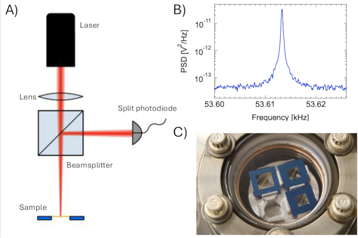
Figure 3: Characterization setup. (A) A cartoon outlining the basic setup and operation of an optical lever. A collimated laser beam is focused onto the sample using a lens. A beamsplitter picks off the retroflected light, directing it to a split photodiode. (B) Example of a thermal PSD signal averaged 50 times with a resolution bandwidth of 0.1 Hz. (C) Resonators rest on a custom aluminum holder, with minimal physical contact, to minimize extrinsic mechanical loss. Please click here to view a larger version of this figure.
Access restricted. Please log in or start a trial to view this content.
Results
We demonstrate the protocol by fabricating a wafer consisting of several 100 nm thick diagonal ribbon resonators34 and characterizing their first few vibrational modes. In this work, the ribbon is 7 mm long and 400 µm wide with 662 µm diameter fillets. We note that while the OL used in this work is naturally suited to torsional modes, it can also detect transverse flexural modes by positioning the beam at a location of non-zero angular deflection. As an illustration, we use the OL to measure both ...
Access restricted. Please log in or start a trial to view this content.
Discussion
One thing that is evident from the data in Figure 5 is that, while the Q of the torsional mode matches the simulated value, the flexural mode Q is lower than predicted. This does not fault the quality of the simulation but rather is a result of neglecting extrinsic loss mechanisms such as substrate mode coupling46 and clamping loss. The dissipation dilution model used in the protocol accounts for all intrinsic loss mechanisms and, therefore, sets an upper bound on the...
Access restricted. Please log in or start a trial to view this content.
Disclosures
The authors declare no competing interests.
Acknowledgements
The authors would like to thank Roland Himmelhuber and the Optical Sciences Micro/Nano Fabrication Cleanroom for use of their facilities and helpful discussions. This work was supported by the National Science Foundation (NSF) through Awards No. 2239735 and No. 2330310. A.R.A. acknowledges support from a CNRS-UArizona iGlobes fellowship, and A.D.H. acknowledges support from a Friends of Tucson Optics Endowed Scholarship. Finally, the reactive ion etcher used for this study was funded by an NSF MRI grant, ECCS-1725571. The protocol was initially developed by A.R.A. and was later modified by A.D.H., C.A.C., and O.A.F. to optimize device fabrication. A.D.H. and D.J.W. co-wrote the manuscript with assistance from all co-authors.
Access restricted. Please log in or start a trial to view this content.
Materials
| Name | Company | Catalog Number | Comments |
|---|---|---|---|
| 100nm double sided Si3N4 on 4'' 200µm Si wafer | WaferPro | Standard Si3N4 wafers used to fabricate membrane resonators | |
| 13KHz Sonificator Quantrex 70 | L&R Ultrasonics | Used in conjunction with acetone to strip contaminants and hardened resist from chip surfaces. | |
| 150 mm glass petri dish, 20 mm deep | Corning Incorporated | 08-747F | For HMDS priming |
| 150 mm plastic petri dish, 15 mm deep | Supertek | S01268 | For wafer transport |
| 2 μm syringe filter | Millipore Sigma | SLAP02550 | For filtering resist particulate |
| 50ml PYREX Griffin Borosilicate Glass Beaker | Corning Incorporated, Life Sciences | General liquid bath containers | |
| Acetone 99.5% ACS grade | Sigma Aldrich | 179124 | General purpose solvent used specifically to strip S1813 resist |
| CarboFib Tweezers | TDI International | TDI 2ACFR-SA | General purpose, chemical-resistant tweezers for safe manipulation of chips in various baths |
| Compressed nitrogen gas cylinder | Locally provided | Drying and cleaning | |
| DI Water | Locally provided | For cleaning chips/wafers by diluting corrosives | |
| Disposable Capillary pipets 7.0-7.4mm | VWR Scientific | For HMDS priming | |
| Emlimny USB Digital Microscope | Emlimney | For the long-distance monitoring of wet etch progress | |
| Hexamethyldisilazane (HMDS) | Sigma Aldrich | 440191 | Wafer primer |
| HiCube HiPace 80 turbopump | Pfeiffer Vacuum | Turbomolecular pump used to pump down sample vacuum chambers | |
| Hydrofluoric Acid 48% | Sigma Aldrich | 695068 | Acid washing and film thinner, diluted to 10% when used |
| ICP-RIE DSE, Versaline DSE III | Plasmatherm | For Si3N4 etching | |
| Isopropanol 99.5% ACS grade | Sigma Aldrich | 190764 | Used to transition released membranes from liquid to air and for cleaning released films |
| Kapton Tape - 1 Mil, 1⁄2" x 36 yds | ULINE | S-7595 | Used for securing wafers and chips to carrier wafers in the plasma etch step |
| LatticeAx 225 | LatticeGear | Cleaving tool | |
| Laurell WS 650 Spin Coater | Laurell Technologies Corporation | Spin coating machine for depositing uniform resist layers on wafers | |
| Mask Less Aligner, MLA150 | Heidelberg Instruments | Photolithography machine  =100nm =100nm | |
| Methanol 99.8% ACS grade | Sigma Aldrich | 179337 | Used to transition released membranes from liquid to air and for cleaning released films |
| MF-319 developer | Kayaku | Developing exposed resist patterns | |
| Microposit S1800 G2 Series Photoresists | Dow Chemical Company | For photolithography patterning. This work specifically uses S1813 resist. | |
| MiniVac Controller | Varian | 9290191 | Vacuum chamber ion pump controller |
| MS-H280-Pro Hot plate | ONiLAB | General heating device | |
| National Instruments NI PXI-1033 | National Instruments | Data acquisition system chassis | |
| Ni PXI-4461 | National Instruments | Analog to digital converter for data acquisition | |
| Potassium Hydroxide KOH Solution 45% | Sigma Aldrich | 417661 | Anisotropic silicon wet etchant |
| Sample Holder | Custom Made | Custom made for holding samples upright in different chemical baths | |
| TLB-6700 Velocity External Cavity Diode Laser | New Focus | 995 | Optical lever laser source |
| Tunable Laser Controller | New Focus | TLB-6700 | Laser controller |
| Vaclon Plus 55 starcell ion pump | Varian | 9191340 | Passice vacuum pump |
| Vacuum chamber | Vacuum chamber for isolating resonators | ||
| Visible quadrant cell photoreceiver | New Focus | 23538-WX | Split photodiode for optical lever readout |
References
- Aspelmeyer, M., Kippenberg, T. J., Marquardt, F. Cavity optomechanics. Rev Mod Phys. 86 (4), 1391-1452 (2014).
- Zwickl, B. M., et al. High quality mechanical and optical properties of commercial silicon nitride membranes. Appl Phys. Lett. 92 (10), 103125(2008).
- Thompson, J. D., et al. Strong dispersive coupling of a high-finesse cavity to a micromechanical membrane. Nature. 452 (7183), 72-75 (2008).
- Wilson, D. J., Regal, C. A., Papp, S. B., Kimble, H. J. Cavity optomechanics with stoichiometric SiN films. Phys Rev Lett. 103 (20), 207204(2009).
- Fedorov, S. A., et al. Generalized dissipation dilution in strained mechanical resonators. Phys Rev B. 99 (5), 054107(2019).
- Engelsen, N. J., Beccari, A., Kippenberg, T. J. Ultrahigh-quality-factor micro- and nanomechanical resonators using dissipation dilution. Nat Nanotechnol. 19 (6), 725-737 (2024).
- Reinhardt, C., Müller, T., Bourassa, A., Sankey, J. C. Ultralow-noise SiN trampoline resonators for sensing and optomechanics. Phys Rev X. 6 (2), 021001(2016).
- Norte, R. A., Moura, J. P., Gröblacher, S. Mechanical resonators for quantum optomechanics experiments at room temperature. Phys Rev Lett. 116 (14), 147202(2016).
- Tsaturyan, Y., Barg, A., Polzik, E. S., Schliesser, A. Ultracoherent nanomechanical resonators via soft clamping and dissipation dilution. Nat Nanotechnol. 12 (8), 776-783 (2017).
- Ghadimi, A. H., et al. Elastic strain engineering for ultralow mechanical dissipation. Science. 360 (6390), 764-768 (2018).
- Fedorov, S. A., Beccari, A., Engelsen, N. J., Kippenberg, T. J. Fractal-like mechanical resonators with a soft-clamped fundamental mode. Phys Rev Lett. 124 (2), 025502(2020).
- Bereyhi, M. J., et al. Perimeter modes of nanomechanical resonators exhibit quality factors exceeding 109 at room temperature. Phys Rev X. 12 (2), 021036(2022).
- Peterson, R. W., et al. Laser cooling of a micromechanical membrane to the quantum backaction limit. Phys Rev Lett. 116 (6), 063601(2016).
- Rossi, M., Mason, D., Chen, J., Tsaturyan, Y., Schliesser, A. Measurement-based quantum control of mechanical motion. Nature. 563 (7729), 53-58 (2018).
- Purdy, T. P., Yu, P. L., Peterson, R. W., Kampel, N. S., Regal, C. A. Strong optomechanical squeezing of light. Phys Rev X. 3 (3), 031012(2013).
- Chen, J., Rossi, M., Mason, D., Schliesser, A. Entanglement of propagating optical modes via a mechanical interface. Nat Commun. 11, 943(2020).
- Kampel, N. S., et al. Improving broadband displacement detection with quantum correlations. Phys Rev X. 7 (2), 021008(2017).
- Mason, D., Chen, J., Rossi, M., Tsaturyan, Y., Schliesser, A. Continuous force and displacement measurement below the standard quantum limit. Nat Phys. 15 (8), 745-749 (2019).
- Hälg, D., et al. Membrane-based scanning force microscopy. Phys Rev Appl. 15 (2), L021001(2021).
- Chowdhury, M. D., Agrawal, A. R., Wilson, D. J. Membrane-based optomechanical accelerometry. Phys Rev Appl. 19 (2), 024011(2023).
- West, R. G., Kanellopulos, K., Schmid, S. Photothermal microscopy and spectroscopy with nanomechanical resonators. J Phys Chem C. 127 (45), 21915-21929 (2023).
- Kristensen, M. B., Kralj, N., Langman, E. C., Schliesser, A. Long-lived and efficient optomechanical memory for light. Phys Rev Lett. 132 (10), 100802(2024).
- Andrews, R. W., et al. Bidirectional and efficient conversion between microwave and optical light. Nat Phys. 10 (4), 321-326 (2014).
- Manley, J., Chowdhury, M. D., Grin, D., Singh, S., Wilson, D. J. Searching for vector dark matter with an optomechanical accelerometer. Phys Rev Lett. 126 (6), 061301(2021).
- Wilson, D. J. Cavity optomechanics with high-stress silicon nitride films. , California Institute of Technology. (2012).
- Norte, R. A. Nanofabrication for on-chip optical levitation, atom-trapping, and superconducting quantum circuits. , California Institute of Technology. (2015).
- Reinhardt, C. Ultralow-noise silicon nitride trampoline resonators for sensing and optomechanics. , McGill University. (2017).
- Ghadimi, A. H. Ultra-coherent nano-mechanical resonators for quantum optomechanics at room temperature. , EPFL. (2018).
- Tsaturyan, Y. Ultracoherent soft-clamped mechanical resonators for quantum cavity optomechanics. , University of Copenhagen, Niels Bohr Institute, Danish Center for Quantum Optics. (2019).
- Sadeghi, P. Study of high-Q nanomechanical silicon nitride resonators. , Technische Universität Wien. (2021).
- Bereyhi, M. Ultra low quantum decoherence nano-optomechanical systems. , EPFL. (2022).
- Agrawal, A. R. Ultra-High-Q Membrane Optomechanics with a Twist. , University of Arizona, Wyant College of Optical Sciences. (2024).
- Barg, A., et al. Measuring and imaging nanomechanical motion with laser light. Appl Phys B. 123, 1-8 (2017).
- Pratt, J. R., et al. Nanoscale torsional dissipation dilution for quantum experiments and precision measurement. Phys Rev X. 13 (1), 011018(2023).
- Pluchar, C. M., Agrawal, A. R., Wilson, D. J. Quantum-limited optical lever measurement of a torsion oscillator. Optica. 12 (3), 418-423 (2025).
- Shin, D. C., Hayward, T. M., Fife, D., Menon, R., Sudhir, V. Active laser cooling of a centimeter-scale torsional oscillator. Optica. 12 (4), 473-478 (2025).
- Manley, J., et al. Microscale torsion resonators for short-range gravity experiments. Phys Rev D. 110 (12), 122005(2024).
- Condos, C. A., et al. Ultralow loss torsion micropendula for chipscale gravimetry. arXiv. , (2024).
- Villanueva, L. G., Schmid, S. Evidence of surface loss as ubiquitous limiting damping mechanism in SiN micro- and nanomechanical resonators. Phys Rev Lett. 113 (22), 227201(2014).
- Yang, C., Pham, J. Characteristic study of silicon nitride films deposited by LPCVD and PECVD. Silicon. 10 (6), 2561-2567 (2018).
- Microposit S1800 G2 Series Photoresists. Technical Datasheet. Technical Datasheet. , Dow Chemical Co. (2024).
- Microposit MS-319 Developer. Technical Datasheet. , Shipley Co. (1997).
- Seidel, H., Csepregi, L., Heuberger, A., Baumgärtel, H. Anisotropic etching of crystalline silicon in alkaline solutions: I. Orientation dependence and behavior of passivation layers. J Electrochem Soc. 137 (11), 3612-3626 (1990).
- Zubel, I., Kramkowska, M. Etch rates and morphology of silicon (hkl) surfaces etched in KOH and KOH saturated with isopropanol solutions. Sens Actuators A Phys. 115 (2-3), 549-556 (2004).
- Metzger, C., Favero, I., Ortlieb, A., Karrai, K. Optical self cooling of a deformable Fabry-Perot cavity in the classical limit. Phys Rev B. 78 (3), 035309(2008).
- de Jong, M. H., et al. Mechanical dissipation by substrate-mode coupling in SiN resonators. Appl Phys Lett. 121 (3), 032201(2022).
- Metzger, C., Favero, I., Ortlieb, A., Karrai, K. Optical self cooling of a deformable Fabry-Perot cavity in the classical limit. Phys Rev B. 78 (3), 035309(2008).
- Moura, J. P., Norte, R. A., Guo, J., Schäfermeier, C., Gröblacher, S. Centimeter-scale suspended photonic crystal mirrors. Opt Express. 26 (2), 1895-1909 (2018).
- Norder, L., et al. Pentagonal photonic crystal mirrors: scalable lightsails with enhanced acceleration via neural topology optimization. Nat Commun. 16 (1), 2753(2025).
- Høj, D., et al. Ultra-coherent nanomechanical resonators based on inverse design. Nat Commun. 12 (1), 5766(2021).
- Shin, D., et al. Spiderweb nanomechanical resonators via Bayesian optimization: inspired by nature and guided by machine learning. Adv Mater. 34 (3), 2106248(2022).
- Gärtner, C., Moura, J. P., Haaxman, W., Norte, R. A., Gröblacher, S. Integrated optomechanical arrays of two high reflectivity SiN membranes. Nano Lett. 18 (11), 7171-7175 (2018).
- Guo, J., Norte, R., Gröblacher, S. Feedback cooling of a room temperature mechanical oscillator close to its motional ground state. Phys Rev Lett. 123 (22), 223602(2019).
- Engelsen, N. J., et al. Optomechanical integration of ultralow dissipation nanomechanical resonators. , Optica Publishing Group. (2022).
- Schilling, R., et al. Near-field integration of a SiN nanobeam and a SiO2 microcavity for Heisenberg-limited displacement sensing. Phys Rev Appl. 5 (5), 054019(2016).
- Wilson, D. J., et al. Measurement-based control of a mechanical oscillator at its thermal decoherence rate. Nature. 524 (7565), 325-329 (2015).
Access restricted. Please log in or start a trial to view this content.
Reprints and Permissions
