This article presents the Frequency Domain Thermoreflectance (FDTR) technique for local nondestructive thermal characterization and imaging.
A subscription to JoVE is required to view this content. Sign in or start your free trial.
Method Article
The Frequency Domain Thermoreflectance Technique for Thermal Property Measurements
In This Article
Summary
Abstract
The frequency domain thermoreflectance (FDTR) technique is a nondestructive method for thermal characterization and imaging with microscale spatial resolution. The technique relies on a pump laser to generate a modulated temperature change in a sample and a probe laser to monitor the sample's local thermal response. The sample's thermal properties are determined by fitting a thermal model to the sample's thermoreflectance response. This article presents detailed protocols for implementing the technique and conducting local measurements of a substrate's local thermal conductivity. Special attention is devoted to discussing how the measurement is influenced by the laser source parameters, error sources in an FDTR measurement, and quantifying the measurement uncertainty. Finally, we discuss a thermal conductivity imaging experiment conducted near a single vertical interface between two surface-activated bonded single-crystal silicon substrates. The thermal conductivity at the interface is suppressed by 3% compared to the bulk value in the adjoining single crystals. The ability to probe interface thermal properties with the FDTR technique may facilitate local studies of heat flow around individual grain boundaries, particularly in thermoelectric materials, where they can be tuned to optimize the performance of thermoelectric devices.
Introduction
Thermal metrology and characterization tools are critical to the design and optimization of advanced materials used in, for example, thermoelectric generators and refrigeration applications1,2. Materials with low thermal conductivity and high electrical conductivity are generally preferred in these applications to maintain a large temperature gradient between hot and cold junctions and for efficient thermal-to-electrical energy conversion. Realizing these disparate properties in bulk crystalline materials is challenging. However, microstructure engineering through the introduction of point and interfacial defects (such as grain boundaries) is a promising direction to design high-performance thermoelectric materials1. A majority of the grain boundary (GB)-controlled thermal conductivity studies have mainly focused on the grain size as the fundamental structural property of importance2,3,4,5, as they lack the spatial resolution to probe a GB's local thermal environment.Thermal metrology at the micro- and nano-scale can provide local information on how heat flows near individual GBs. For example, recent microscale thermal imaging measurements by Isotta et al.6,7 revealed that the bulk thermal conductivity (κ) is locally suppressed near individual GBs in polycrystalline tin telluride (SnTe) and silicon. The observed κ suppression was correlated with different GB properties, including misorientation angle, roughness of the GB plane, nanotwinning density, and porosity. These types of measurements can facilitate tuning the bulk κ by providing local information on the microstructure-κ relationship. As interest in the local effects of defects on κ continues to grow, both computational8 and experimental9,10 approaches that provide insight into these contributions will become increasingly relevant.
Optical thermoreflectance methods11,12,13,14,15 are widely used for nondestructive thermal metrology of bulk solids, thin film superlattices, and interfaces. The methods use ultrafast or intensity-modulated lasers to locally heat a sample and probe their thermal response with high frequency or temporal resolution16, making them ideal for characterizing thermophysical properties. Thermoreflectance techniques, including time-domain thermoreflectance (TDTR)13,16 and frequency-domain thermoreflectance (FDTR)17,18, are the most common high-resolution thermal metrology methods. FDTR uses a focused intensity-modulated pump laser to generate a local periodic heat source in the sample. The resulting sample temperature change is transduced into a modulation frequency-dependent thermoreflectance signal that is recorded with a lock-in amplifier. To facilitate the measurement, a thin transducer layer with a large thermoreflectance coefficient19 at the probe laser wavelength is deposited on the sample. The TDTR technique, on the other hand, utilizes ultrafast pump and probe lasers, and the transient thermoreflectance signal of the transducer layer is monitored at different time delays between the pump and probe lasers, with picosecond time resolution.
Thermoreflectance techniques offer microscale lateral spatial resolution for probing thermophysical properties, and the measurements can be configured to characterize both isotropic and anisotropic κ of materials. Recently, Sood et al.10 used the TDTR technique to map local κ inhomogeneities in boron-doped polycrystalline diamond that were correlated with electron-backscatter diffraction imaging. In their measurements, regions in the sample with small grains had a lower κ compared to the bulk value. However, their measurements did not show whether the κ suppression was due to the small grain sizes or resistive GBs. Following this work, Isotta et al. showed that the local κ suppression around individual GBs, observed in microscale FDTR maps of SnTe, a mid-temperature thermoelectric material, is directly correlated to the GB misorientation angle6, so far only predicted theoretically 20,21,22,23 or rarely measured in fabricated GBs 24. Compared to the TDTR approach used by Sood et al., FDTR is less expensive and allows for the measurement of multiple properties, such as the substrate κ and constant-pressure heat capacity (C), and the film-substrate interface thermal conductance, in a single measurement that spans a broad frequency range25. Two-dimensional thermoreflectance phase maps obtained at multiple pump laser modulation frequencies with the highest sensitivity to the sample's thermal properties are converted to a κ image.
The thermoreflectance phase represents the phase shift between the periodic temperature oscillations at the surface of a transducer layer and the modulated heat source produced by the absorbed pump laser. In a standard FDTR approach, the pump and probe lasers are focused to the same point on the sample surface, and the thermoreflectance phase at that point is measured with a lock-in amplifier at different pump laser modulation frequencies. A layered heat conduction model is fitted to the measured data to determine the sample's thermal properties (i.e., κ, C, and the transducer-sample interface conductance)14. Variations of the standard FDTR approach allow for improved sensitivity of the measured thermoreflectance phase to the sample's anisotropic κ. These include the use of (i) spatially offset pump and probe lasers26, (ii) elliptical27 or line28 shaped pump laser-generated heat sources, and (iii) FDTR measurements with variable pump laser spot sizes29. Beyond thermal characterization of bulk properties, the FDTR technique can be used to characterize interface thermal properties30,31,32,33,34,35, since the thermal penetration depth of the heat source, defined as 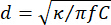 depends on the pump laser modulation frequency (f). The interface causes a thermal resistance due to the transmission and reflection of heat carriers (i.e., electrons and phonons)36. The resistance is characterized in FDTR experiments in terms of an interface thermal conductance. FDTR measurements of the interface thermal conductance of self-assembled monolayers33,35, metal-substrate interfaces37,38,and thin interface layers39 have been reported in the literature. Finally, FDTR measurements with thin magnetic transducer films were recently shown to allow for the characterization of anisotropic κ of two-dimensional materials40.
This article provides a detailed description of the procedures involved in a FDTR measurement that utilizes coaxially focused pump and probe lasers on the transducer surface. Representative measurements of local κ of a bulk silicon substrate are provided, and the measurement uncertainties are quantified. Finally, we provide a simple example that illustrates the FDTR imaging of the local κ near a single vertical interface between two (100) single-crystal silicon substrates bonded by surface activated bonding (SAB).
Access restricted. Please log in or start a trial to view this content.
Protocol
1. FDTR system setup
NOTE: A schematic diagram of the experimental setup is shown in Figure 1, and the associated commercially available components are listed in the Table of Materials. The following steps describe the installation of the pump and probe lasers, as well as the signal acquisition system.
- Begin by installing a low-power (1 mW) electroabsorptive intensity modulated diode laser (EML) with a fundamental wavelength of 1550 nm. Install the EML on a butterfly laser diode mount that is integrated with a laser diode current and temperature controller (LDC). Ensure good thermal contact between the EML and butterfly mount by using a thermally conductive paste (silver paste, for example), such that the thermoelectric cooler (TEC) in the EML can effectively maintain the diode laser temperature. Set the appropriate laser diode current in the LDC to control the output power of the EML. Turn on the TEC controller in the LDC and allow up to 10 min for the EML temperature to stabilize at the appropriate value before turning on the LDC diode current supply to the EML.
NOTE: This is the pump laser. The 1550 nm wavelength is absorbed strongly by the gold transducer. - To modulate the diode laser intensity, drive the EML with a voltage-biased sinusoidal radio frequency (RF) signal, with frequencies between 100 kHz and 80 MHz. Split the output voltage from the RF signal generator and send half of the signal to the reference port of a lock-in amplifier. Send the other half of the signal to a bias tee along with a separate bias voltage, and connect the output port of the bias tee to the EML.
NOTE: The use of a bias tee may be optional depending on the specifications of the diode laser; the primary goal of this setup is to modulate the output intensity of the EML. - To amplify the output of the EML, feed the fiber optical output from the EML to a 5 W fiberized erbium-doped fiber amplifier (EDFA). The output of the EDFA is the pump laser for the FDTR setup. Control the pump laser power from the EDFA to achieve the desired intensity at the sample surface.
- Collimate the output light from the EDFA fiber using an appropriate lens. To prevent back-reflections from various free-space optics in the FDTR setup into the EDFA, direct the transmitted light from the collimator into a Faraday optical isolator.
- Direct the output beam from the isolator to the sample surface through a 4-f optical imaging system, comprised of a Gimbal scanning mirror, two relay lenses, and a microscope objective. Since the pump laser wavelength is in the infrared region of the electromagnetic spectrum, and as such, the laser is not visible, use a fluorescent card to align the pump laser through the 4-f imaging system and collinear with the probe laser along the optical axis of the microbench.
NOTE: The 4-f imaging system images the center of the scanning mirror to the back aperture of the objective. This allows for scanning the focused pump laser transmitted through the microscope objective on the sample surface, by changing the entry angle of the light into the back aperture of the objective without translating the input beam on the microscope aperture. - Next, mount the probe laser, which is a frequency-doubled neodymium-doped yttrium aluminum garnet (Nd-YAG) continuous wave diode laser, on a passively cooled mount. The maximum probe power and wavelength are 50 mW and 532 nm, respectively. Similar to the pump laser, direct the probe diode laser output through a Faraday optical isolator. Also, use a two-lens system to adjust the collimated beam size of the laser exiting the isolator.
- Place a half-wave plate in the beam path of the probe laser, followed by a polarizing beam splitter (PBS); this configuration serves as a variable attenuator, which allows the user to control the optical power delivered to the sample. Direct the output of the variable attenuator through a quarter-wave plate before the light reaches the microscope objective. Rotate the fast axis of this quarter-wave plate by 45 degrees relative to the polarization direction of the probe laser, which effectively rotates the light's polarization by 90 degrees on two passes through the optic.
NOTE: This ensures that the reflected probe light from the sample surface is redirected to a high-speed photodetector and not back to the diode laser. - Deliver the probe laser to the center of the microscope objective coaxially with the pump laser. Align the pump and probe lasers along the optical axis of a micro-bench setup to ensure that the two beams remain coaxial going through the objective.
NOTE: Proper alignment is critical to ensure that the pump and probe lasers remain along the optical axis of the microbench and collinear between the focal planes of the pump and probe lasers.
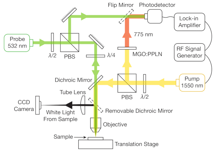
Figure 1: Schematic of the FDTR experimental setup.Please click here to view a larger version of this figure.
- To read the thermoreflectance signal delivered to the photodetector by the probe laser, feed the photodetector output to a lock-in amplifier. Ensure that the frequency response of the photodetector and lock-in amplifier allows for measurement of modulated signals at the pump laser modulation frequency.
- Record the pump laser power at the sample location. Place a power meter beneath the microscope objective and read the power level of the pump laser while the probe laser is blocked.
- To image the sample surface, direct the reflected light from the sample through a tube lens to a CCD camera, where the image of the sample surface is formed. Place a removable dichroic (cold) mirror between the microscope and the tube lens to direct the reflected light from the sample surface to the CCD camera.
NOTE: The cold mirror must be removed when conducting measurements - it is only used when observing the sample surface with the CCD camera. The following steps require an understanding of the signal analysis process. The phase of the modulated thermoreflectance, which is the sample surface-temperature dependent probe laser intensity, is the critical signal of interest in an FDTR measurement. The lock-in amplifier records the amplitude and phase of the thermoreflectance signal. However, other unwanted signal sources are mixed with the thermoreflectance phase. Specifically, the phase signal ((ϕsample) includes a combination of the sample's thermoreflectance phase (ϕTR), the phase shift associated with the optical path distance (OPD) traveled by the probe laser from the sample surface to the photodetector (ϕOPD), and additional phase noise contributions arising from the detection electronics (ϕnoise). To eliminate the OPD and noise contributions to the detected phase, one must implement a secondary beam path as a reference which, when detected, contains both ϕOPD and ϕnoise but not ϕTR. In this way, the thermoreflectance phase can be extracted from the probe signal (ϕsample) by subtracting the reference phase: ϕTR = ϕsample - ϕref. This concept is illustrated in Figure 2A, where both ϕsample and ϕref are measured relative to the RF signal provided by the RF signal generator to the lock-in amplifier. An example of this phase subtraction step with real phase data is provided in Figure 2B. When building the reference beam path, one must incorporate three critical steps: (1) match the optical path distance to the distance traveled by the probe laser from the sample surface to the photodetector, (2) detect the reference beam using the same photodetector as the sample signal, and (3) modulate the reference beam intensity using the same RF signal that modulates the pump laser. We remark that the photodetector is not responsive to the pump laser wavelength and the reflected pump beam does not make it to the visible photodetector. As such, the reflected pump light from the sample surface does not affect the thermoreflectance phase.
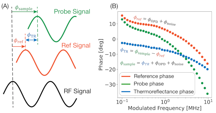
Figure 2: The thermoreflectance phase calculated by subtracting the reference signal phase from the probe signal phase. These phase shifts are depicted conceptually in (A), and an example with real point measurement data is shown in (B).Please click here to view a larger version of this figure.
- Split off a portion of the pump beam to generate the reference beam, thus fulfilling requirement (3). Please refer to the above NOTE. Do this by installing a half-waveplate and PBS as a variable attenuator (following the same procedure described in step 1.6) in the beam path, where the light that the PBS reflects is used as the reference beam.
- Since the pump laser (1550 nm) cannot be detected by the visible-light detector that detects the probe laser (532 nm), next pass the reference beam through a periodically poled lithium niobate (PPLN) second harmonic generation (SHG) crystal to produce a 775 nm beam. This fulfills requirement (2).
- Build the optical path from the PPLN crystal output (the point of 775 nm wave generation) to the photodetector to have the same length as the optical path distance traversed by the probe laser between the sample surface and the photodetector. Install an optical delay line in the optical path of the probe beam to precisely control the OPD of the reflected probe (532 nm) laser relative to the reference (775 nm) laser. Use a calibration sample, such as a gold thin film on a silicon substrate, with known properties, and move the delay line to match the measured thermoreflectance phase over the frequency range of interest to thermal model calculations.
- Ensure that the PPLN crystal temperature is set to optimize the generated power output by adjusting the setting on the crystal's PID controller until the photodetector signal amplitude is maximized.
2. Sample preparation
NOTE: To conduct a successful FDTR experiment, the sample's surface must be polished to a mirror-like finish to reduce diffuse reflections and any height variations that may cause the laser defocusing or changes to the specularity of the reflected probe beam, while scanning across the surface. After this point, the metal transducer layer must be deposited and characterized.
- Polish the sample using suspensions of gradually smaller particle sizes until a mirror-like finish is achieved. For example, use a series of diamond suspensions with particle sizes ranging from 5 μm to 250 nm. Finish with a suspension of colloidal silica, polishing until a mirror-like finish is achieved.
NOTE: The specific duration of each polishing step and particle size will depend on the sample. - As a final cleaning step, ion-mill the surface for 10 min.
- Measure the root-mean-square roughness of the surface using atomic force microscopy (AFM); the rms roughness should be below 20 nm.
- After polishing, deposit a metal transducer layer on the sample surface. For a 532 nm probe laser, apply a gold thin film as the transducer layer due to its large thermoreflectance coefficient19. For the smoothest transducer surface, use an electron beam (e-beam) evaporator to coat a uniform gold layer on the sample with a layer thickness greater than 40 nm. For atomic force microscopy (AFM) measurements of the transducer thickness, tape a sliver of thin glass onto the sample surface to serve as a shadow mask before placing the sample into the e-beam evaporator. Then, complete the gold deposition.
NOTE: The transducer must be thicker than the optical skin-depth of gold (≈20 nm for 532 nm light), but ideally thicker than twice the optical skin-depth to give a sufficiently strong reflected signal. - Measure the thickness of the gold layer using the picosecond ultrasonic method41 (Figure 3A), AFM, or any other technique with sufficient resolution. If using AFM, then scan the AFM probe over the sharp gold edge generated by the shadow mask; this step height is the gold thickness.
- If the gold's thermal conductivity is not known, conduct a van der Pauw measurement42 on a gold film deposited on an insulating substrate, such as glass. Alternatively, conduct an FDTR measurement of the gold layer deposited on a standard substrate of known thermal conductivity.
NOTE: The thermal conductivity of gold is known to vary slightly as a function of film thickness43.
3. Measurement setup
- Turn the power switch of the 532 nm diode laser to the on position to activate the power supply. Wait until the enable light turns on, at which point the laser crystal's temperature stabilizes, and turn the laser switch to initiate the emission of the 532 nm laser. An input probe laser power of 20-30 mW is sufficient for detecting the thermoreflectance signal. Use a power meter to ensure the laser power falls within that range before proceeding.
- Turn on the pump laser diode controller, and enable thermoelectric cooling by setting the appropriate resistance value according to the diode laser specifications (e.g., 10 kΩ). Once the temperature has stabilized, turn on the laser current.
- Turn on the EDFA and set the output power to a desired value (e.g., 1 W).
NOTE: This value should be selected based on the thermal diffusivity and melting point of the sample material. Keep in mind that the power delivered to the sample is less than the power set at the fiber amplifier (see step 1.10 to measure the power at the sample location). The amount of absorbed power can be estimated based on the pump wavelength and the transducer absorbance. - Set the RF frequency, RF amplitude, and bias voltage at the signal generator(s) to modulate the pump laser intensity.
- Turn on the lock-in amplifier and photodetector. Ensure that the reference port is connected to the RF signal generator output and the signal input port is connected to the photodetector.
- Turn on the temperature controller for the PPLN crystal and enable the PID control.
- Mount the sample on the multi-axis precision stage that has a micrometer knob to adjust the stage height (Z-position). Adhere the sample to the stage using thin double-sided tape to prevent the sample from sliding during the measurement.
- Focus the lasers on the sample surface. Begin by mounting the cold mirror above the objective and observing the sample surface through the CCD camera (see step 1.10). Adjust the Z-knob on the stage until the sample surface comes into focus on the live camera feed. Continue to focus until the laser spot is at its minimum size. Once complete, remove the cold mirror.
NOTE: The purpose of this step is to position the sample surface at the desired focal plane. For example, the probe focal plane is found by focusing the probe laser to the smallest spot size on the sample surface. - Next, ensure that the pump and probe lasers are focused on the same point on the sample. Using the requisite LabVIEW virtual instrument (VI), adjust the tilt angles of the Gimbal steering mirror (see step 1.5) until the pump laser is aligned along the optical axis of the probe laser. Look for a maximum thermoreflectance amplitude to know when the lasers are coincident on the sample surface.
4. Spot size measurement
NOTE: Thermoreflectance measurements of thermal properties are known to demonstrate extreme sensitivity to the measured spot size17. Below is a procedure to conduct a spot size measurement of either the pump or probe laser. General steps which apply to both lasers are provided in 4.1 - 4.6, and then special considerations for the individual pump and probe lasers are provided in steps 4.7 - 4.10.
- Acquire a "knife's edge" sample, consisting of gold patterns deposited on a glass.
NOTE: Standard samples can be purchased, or fabricated via photo- or electron beam lithography to ensure a sufficiently sharp interface. - Mount the sample on the multi-axis translation stage (see step 3.7).
- Position the sample such that the laser spot is close to the desired gold edge, with the edge aligned perpendicular to the desired scan direction (either x or y). Move the sample manually or with a separate large-area translation stage, and then fine-tune the position using the knobs on the stage. Do not use these knobs for large area adjustments, as it is important for the translation stage axes to be centered during the scanning measurement.
NOTE: If the stage position is off-center during the measurement, there can arise a coupling between multiple axes that skews the sample position and potentially moves the sample out of the focal plane. - Complete the FDTR system initialization, focusing, and laser alignment procedures, as detailed in the Measurement setup section of the protocol (steps 3.1 to 3.10).
- Turn on the translation stage controller, zero each motion-control actuator, and enter the controller's identification number into the LabVIEW VI.
- In the VI, enter the desired scan length in the primary scan direction (denoted "A") and the number of desired line scans in the "B" direction. Enter the step size in each direction.
NOTE: A typical line scan might span a 20-100 μm length with a 0.2-1 μm step size, depending on the size of the laser spot. - Scan the knife's edge interface and record the reflected light intensity signal. Process the data using the "SpotSizeFit.py" code to calculate the laser spot radius. The code is provided in the supporting material.
NOTE: Either the reflected or transmitted light can be detected, whichever is most convenient for a given setup. - Repeat steps 4.3-4.7, scanning across a sharp gold edge in the direction perpendicular to the previous scan. Calculate the average spot radius and standard deviation between the perpendicular scan directions.
NOTE: The laser spot should have an eccentricity close to 1. Also, given the wavelengths of each laser and the modulation scheme described in steps 1.1 to 1.15, some additional considerations are specific to the measurements of each laser: (1) The pump laser (1550 nm) requires an infrared (IR) detector, as it cannot be detected using the visible light detector. (2) The RF signal generator does not directly modulate the probe laser, and thus requires a separate modulation, which can be achieved by mechanical chopping. However, this introduces a third consideration: (3) Mechanical choppers do not operate at radio frequencies, and so the chopped probe signal cannot be captured by the same lock-in amplifier as the RF-modulated signals. (For example, the SR844 lock-in amplifier has a low-frequency cutoff at 20 kHz.) These three considerations are addressed in the following steps. - Install an IR photodetector and direct a portion of the pump beam reflecting from the sample to this detector. For example, some of the reflected beam will emerge from the PBS installed in step 1.9, and this beam can be directed to the IR photodetector.
- Install a mechanical chopper in the probe beam path, mounted on a vibration-damping foam.
- Before beginning a pump spot size measurement, first connect the RF signal to the SR844 lock-in amplifier's reference port, and the IR photodetector to the SR844 lock-in amplifier's input port.
- Before beginning a probe spot size measurement, first connect the mechanical chopper's controller output to the SR830 lock-in amplifier's reference port, and the visible light photodetector to the SR830 lock-in amplifier's input port.
- Run each spot size measurement (pump or probe) using the requisite "read" VI for the given lock-in amplifier.
5. Point measurements
NOTE: Point measurements are used to measure the local thermal properties at a single point on the sample surface. Typically, the substrate material's thermal conductivity and the interface thermal conductance between the gold transducer and the substrate are measured. These properties are considered an average measurement over an area spanning the effective spot size of the pump and probe lasers13,17.
- Mount the sample on the multi-axis translation stage (see step 3.7).
- View the sample through the CCD camera and adjust its placement to ensure the probe laser is reflected at a clear spot free of dirt and other impurities.
- Select the pump power level and complete the focus and alignment procedure detailed in steps 3.1 to 3.10.
- Decide on the frequency range for the point measurement. Ensure that the thermal diffusion model is sensitive and appropriate for the measured properties in this frequency range.
- Select the appropriate sensitivity level on the lock-in amplifier for the measurement frequency range. Program the point measurement LabVIEW VI with the lock-in sensitivity level, frequency range, and total number of frequencies to be measured. If needed, program multiple stages with different sensitivity levels to maximize the signal-to-noise ratio (SNR).
- Run the point measurement and save the data to a .txt file. Record the phase data from the lock-in amplifier three times, for (1) the probe laser signal, (2) the reference laser signal, and (3) the noise. Always block the beam that is not being measured, and block both probe and reference beams to record the noise data.
- To account for instrument or environmental noise, repeat steps 5.2-5.5 and average the fitted results.
6. Image measurements
NOTE: Thermal property images are two-dimensional maps of the measured thermal properties over an area, created by scanning the lasers over the sample surface and collecting an array of point measurements.
- Begin by mounting the sample on the multi-axis translation stage (see step 3.7) and position the laser spot over the measurement area by monitoring the CCD camera. Check that the region is free of dirt and irregularities in roughness.
NOTE: Avoid moving the translation axes of the stepper motor stage to their extremes to avoid coupling with the Z-axis. See step 4.3. - Program the measurement area into the image measurement LabVIEW VI. Run a quick scan over the measurement area (e.g., three steps in both x and y directions) while monitoring the CCD camera live feed, and make note of the precise measurement area.
- Select the pump power level and complete the focus and alignment procedure described in steps 3.7-3.10 in Protocol 3.
- Select at least five frequencies at which to scan the sample. Ensure that the thermal model is sensitive to the measured properties in this frequency range.
- Block the probe laser and record the in-phase (i.e., X) and quadrature (i.e., Y) readings from the lock-in amplifier display for the reference laser. Then block both the probe and reference lasers to record the X and Y noise readings. When complete, unblock the probe laser.
- Select the number of steps (i.e., the number of point measurements) in each scan direction (x and y) in the LabVIEW VI. Run the map measurement.
- Repeat step 6.5 when the measurement has finished. Calculate the average X and Y from before and after the measurement, for both the reference signal and the noise signal.
NOTE: Reference and noise measurements could be collected at each measurement location in the scan, but this would significantly increase the time required for each image measurement. By averaging these quantities from two measurements (one before and one after the spatial scan), the total measurement time is significantly reduced. By following the procedural steps described in the Protocol section, users can build an FDTR system, prepare samples for thermal characterization, and conduct point and image measurements of local κ. In the following section, we demonstrate measurements of local κ on a single-crystal silicon substrate that use these protocols and comment on the sources of uncertainty and limitations to the FDTR implementation.
Access restricted. Please log in or start a trial to view this content.
Results
Point measurements
The goal of the point measurement presented here is to determine the room-temperature thermal conductivity (κ) of (100) single-crystal silicon based on the measured thermoreflectance phase of the gold transducer film on the sample. A two-layer heat conduction model is fitted to the measured phase data to determine the best-fit substrate κ and the transducer-silicon interface thermal conductance (G). The measured transducer thickness, thermal conduct...
Access restricted. Please log in or start a trial to view this content.
Discussion
The FDTR technique presented here is used to characterize the local substrate κ of a single-crystal silicon substrate and to map the κ distribution around an interface between two plasma-sintered silicon substrates. One critical aspect of the measurement is the use of the modeling fitting to determine the unknown thermal properties of the substrate and the transducer-substrate interface. The accuracy of the measurement depends on the proper selection of the spot size and modulation frequencies of the pump laser...
Access restricted. Please log in or start a trial to view this content.
Disclosures
The authors disclose no conflicts of interest.
Acknowledgements
Some of the authors were supported by partial funding from the Northwestern University Center for Engineering Sustainability and Resilience through a seed-funded project entitled "Toward Engineering Metamaterials for Sustainable Energy Solutions: Local Thermal Properties of Grain Boundaries in Polycrystalline Materials".
Access restricted. Please log in or start a trial to view this content.
Materials
| Name | Company | Catalog Number | Comments |
|---|---|---|---|
| 3-Axis NanoMax Stage, Stepper Motor Drives | Thorlabs | MAX383 | Sample translation stage |
| 532 nm Continuous Wave Laser | SpectraPhysics | SPFL 532-20 | Probe laser |
| Achromatic Doublet, f=150mm, 2" | Thorlabs | AC508-150-C-ML | Relay lenses in the 4-f optical imaging system used to image the center of the Gimbal scanner to the back aperture of the microscope objective |
| Beamsplitter Cube | Thorlabs | BS019 | Optics |
| Broadband Power/Energy Meter | Melles Griot | 13PEM001 | To measure laser powers |
| Closed-Loop Picomotor Controller | New Focus | 8743-CL | For scanning the pump beam on the sample surface |
| Color CMOS Camera | Thorlabs | CS165CU1 | For imaging the sample surface |
| Current-Limited Power Supply | New Focus | 901 | To power the high-speed photodetector |
| Fiber Amplifier | IPG Photonics | LDR-3U | Pump laser |
| Free-Space Isolator, 1550 nm | Thorlabs | IO-5-1550-HP | For preventing back reflections of the pump laser into the fiber amplifier |
| Free-Space Isolator, 532 nm | Thorlabs | IO-3-532-LP | For preventing back reflections of the probe laser into the diode laser |
| Function / Arbitrary Waveform Generator | Agilent | 33220A | For modulating the pump laser intensity |
| Gimbal Optic Mount | Newport | 605-2 | For scanning the pump beam on the sample surface |
| Gold Mirrors, 1" | Thorlabs | PF10-03-M01 | High reflectivity mirrors for the pump laser |
| Half Waveplate (1550) | Thorlabs | WPH05M-1550 | Polarization optics |
| Half Waveplate (532 nm) | Thorlabs | Polarization optics | |
| IR 1 GHz Low Noise Photoreceiver | New Focus | 1611 | For monitoring the modulated intensity of the pump laser |
| Laser Diode Controller | ILX Lightwave | LDC-3742B | For controlling the seed pump laser intensity |
| Lock-In Amplifier | Stanford Research Systems | SR844 | For high-frequency measurements |
| Lock-In Amplifier | Stanford Research Systems | SR830 | For low-frequency measurements |
| Mechanical Chopper Controller | Stanford Research Systems | SR540 | For modulating the probe beam intensity |
| MgO:PPLN Crystal | Covesion | Second harmonic generation crystal for frequency doubling the 1550 nm pump laser to the 775 nm reference light source | |
| Polarizing Beamsplitter Cube | Thorlabs | PBS254 | Polarization optics |
| RF Signal Generator | Agilent | N9310A | For modulating the pump laser intensity |
| Stepper Motor Controller | Thorlabs | BSC200 | Controller for the sample translation stage |
| Temperature Controller | Covesion | OC1 | For controlling the MgO:PPLN Crystal temperature |
| Visible 1 GHz Low Noise Photoreceiver | New Focus | 1601 | For monitoring the thermoreflectance signal |
References
- Rahman, J. U., et al. Grain boundary engineering enhances the thermoelectric properties of YTe. Adv Energy Mater. 15, 2404243(2025).
- Villoro, R. B., et al. Grain boundary phases in NbFeSb half-Heusler alloys: a new avenue to tune transport properties of thermoelectric materials. Adv Energy Mater. 13, 2204321(2023).
- Meng, X. F., et al. Grain boundary engineering for achieving high thermoelectric performance in n-type skutterudites. Adv Energy Mater. 7, 1602582(2017).
- Villoro, R. B., et al. Fe segregation as a tool to enhance electrical conductivity of grain boundaries in Ti(Co,Fe)Sb half-Heusler thermoelectrics. Acta Mater. 249, 118816(2023).
- Biswas, K., et al. High-performance bulk thermoelectrics with all-scale hierarchical architectures. Nature. 489, 414-418 (2012).
- Isotta, E., et al. Microscale imaging of thermal conductivity suppression at grain boundaries. Adv Mater. 35, 2302777(2023).
- Isotta, E., et al. Heat transport at silicon grain boundaries. Adv Funct Mater. 34, 2405413(2024).
- Yeandel, S. R., Molinari, M., Parker, S. C. The impact of tilt grain boundaries on the thermal transport in perovskite SrTiO-layered nanostructures: a computational study. Nanoscale. 10, 15010-15022 (2018).
- Alikin, D., et al. Nanoscale imaging and measurements of grain boundary thermal resistance in ceramics with scanning thermal wave microscopy. ACS Appl Mater Inter. 16, 42917-42930 (2024).
- Sood, A., et al. Direct visualization of thermal conductivity suppression due to enhanced phonon scattering near individual grain boundaries. Nano Lett. 18, 3466-3472 (2018).
- Cahill, D. G., Goodson, K. E., Majumdar, A. Thermometry and thermal transport in micro/nanoscale solid-state devices and structures. J Heat Trans ASME. 124, 223-241 (2002).
- Olson, D. H., Braun, J. L., Hopkins, P. E. Spatially resolved thermoreflectance techniques for thermal conductivity measurements from the nanoscale to the mesoscale. J Appl Phys. 126, 150901(2019).
- Jiang, P. Q., Qian, X., Yang, R. Tutorial: time-domain thermoreflectance (TDTR) for thermal property characterization of bulk and thin-film materials. J Appl Phys. 124, 161103(2018).
- Sandell, S., et al. Thermoreflectance techniques and Raman thermometry for thermal property characterization of nanostructures. J Appl Phys. 128, 131101(2020).
- Chen, T., Jiang, P. Q. Decoupling thermal properties in multilayered systems for advanced thermoreflectance experiments. Phys Rev Appl. 23, 044004(2025).
- Giri, A., et al. Ultrafast and nanoscale energy transduction mechanisms and coupled thermal transport across interfaces. ACS Nano. 17, 14253-14282 (2023).
- Schmidt, A. J., Cheaito, R., Chiesa, M. A frequency-domain thermoreflectance method for the characterization of thermal properties. Rev Sci Instrum. 80, 094901(2009).
- Saurav, S., Mazumder, S. On the determination of thermal conductivity from frequency-domain thermoreflectance experiments. J Heat Trans ASME. 144, 013501(2022).
- Wilson, R. B., et al. Thermoreflectance of metal transducers for optical pump-probe studies of thermal properties. Opt Express. 20, 28829-28838 (2012).
- Dong, H. C., Wen, B., Melnik, R. Relative importance of grain boundaries and size effects in thermal conductivity of nanocrystalline materials. Sci Rep UK. 4, 7037(2014).
- Nan, C. W., Birringer, R. Determining the Kapitza resistance and the thermal conductivity of polycrystals: a simple model. Phys Rev B. 57, 8264-8268 (1998).
- Schelling, P. K., Phillpot, S. R., Keblinski, P. Kapitza conductance and phonon scattering at grain boundaries by simulation. J Appl Phys. 95, 6082-6091 (2004).
- Smith, D. S., et al. Grain boundary thermal resistance and finite grain size effects for heat conduction through porous polycrystalline alumina. Int J Heat Mass Tran. 121, 1273-1280 (2018).
- Xu, D., et al. Thermal boundary resistance correlated with strain energy in individual Si film-wafer twist boundaries. Mater Today Phys. 6, 53-59 (2018).
- Ziade, E. Wide-bandwidth frequency-domain thermoreflectance: volumetric heat capacity, anisotropic thermal conductivity, and thickness measurements. Rev Sci Instrum. 91, 124901(2020).
- Rodin, D., Yee, S. K. Simultaneous measurement of in-plane and through-plane thermal conductivity using beam-offset frequency-domain thermoreflectance. Rev Sci Instrum. 88, 014902(2017).
- Li, M., Kang, J. S., Hu, Y. J. Anisotropic thermal conductivity measurement using a new asymmetric-beam time-domain thermoreflectance (AB-TDTR) method. Rev Sci Instrum. 89, 084901(2018).
- Perez, L. A., et al. Anisotropic thermoreflectance thermometry: a contactless frequency-domain thermoreflectance approach to study anisotropic thermal transport. Rev Sci Instrum. 93, 034902(2022).
- Jiang, P. Q., Qian, X., Yang, R. G. Time-domain thermoreflectance (TDTR) measurements of anisotropic thermal conductivity using a variable spot-size approach. Rev Sci Instrum. 88, 074901(2017).
- Liu, J., et al. Ultralow thermal conductivity of atomic/molecular layer-deposited hybrid organic-inorganic zincone thin films. Nano Lett. 13, 5594-5599 (2013).
- Ota, A., et al. Enhancing thermal boundary conductance of graphite-metal interface by triazine-based molecular bonding. ACS Appl Mater Inter. 11, 37295-37301 (2019).
- Giri, A., et al. Heat-transport mechanisms in molecular building blocks of inorganic/organic hybrid superlattices. Phys Rev B. 93, 115310(2016).
- Losego, M. D., et al. Effects of chemical bonding on heat transport across interfaces. Nat Mater. 11, 502-506 (2012).
- Majumdar, S., et al. Vibrational mismatch of metal leads controls thermal conductance of self-assembled monolayer junctions. Nano Lett. 15, 2985-2991 (2015).
- Lu, B., et al. Cross-plane thermal conductance of phosphonate-based self-assembled monolayers and self-assembled nanodielectrics. ACS Appl Mater Inter. 12, 34901-34909 (2020).
- Chen, J., et al. Interfacial thermal resistance: past, present, and future. Rev Mod Phys. 94, 025002(2022).
- Yuan, C., et al. A review of thermoreflectance techniques for characterizing wide bandgap semiconductors' thermal properties and devices' temperatures. J Appl Phys. 132, 220701(2022).
- Monachon, C., et al. Thermal boundary conductance: a materials science perspective. Annu Rev Mater Res. 46, 433-463 (2016).
- Scott, E. A., et al. Thermal conductivity and thermal boundary resistance of atomic layer deposited high-dielectric aluminum oxide, hafnium oxide, and titanium oxide thin films on silicon. APL Mater. 6, 058302(2018).
- Rahman, M., et al. Simultaneous measurement of anisotropic thermal conductivity and thermal boundary conductance of two-dimensional materials. J Appl Phys. 126, 205103(2019).
- Maris, H. Picosecond ultrasonics. Sci Am. 278, 86-89 (1998).
- Hemenger, P. M. Measurement of high-resistivity semiconductors using Vanderpauw method. Rev Sci Instrum. 44, 698-700 (1973).
- Schmidt, A. J., et al. Characterization of thin metal films via frequency-domain thermoreflectance. J Appl Phys. 107, 024908(2010).
- Schmidt, A. J., et al. A frequency-domain thermoreflectance method for the characterization of thermal properties. Rev Sci Instrum. 80, 094901(2009).
- Tang, L., Dames, C. Anisotropic thermal conductivity tensor measurements using beam-offset frequency-domain thermoreflectance (BO-FDTR) for materials lacking in-plane symmetry. Int J Heat Mass Tran. 164, 120600(2021).
- Stevens, R. J., Smith, A. N., Norris, P. M. Measurement of thermal boundary conductance of a series of metal-dielectric interfaces by the transient thermoreflectance technique. J Heat Trans ASME. 127, 315-322 (2005).
- Yang, J., Ziade, E., Schmidt, A. J. Uncertainty analysis of thermoreflectance measurements. Rev Sci Instrum. 87, 014901(2016).
- Wilson, R. B., Cahill, D. G. Anisotropic failure of Fourier theory in time-domain thermoreflectance experiments. Nat Commun. 5, 5075(2014).
- Isotta, E., et al. A thermal boundary resistance model via mean free path suppression functions and a Gibbs excess approach. Int J Heat Mass Tran. 252, 127417(2025).
- Sakata, M., et al. Thermal conductance of silicon interfaces directly bonded by room-temperature surface activation. Appl Phys Lett. 23, 106(2015).
- Xiang, Z. Y., Jiang, P. Q., Yang, R. G. Time-domain thermoreflectance (TDTR) data analysis using phonon hydrodynamic model. J Appl Phys. 132, 205104(2022).
- Beardo, A., et al. Phonon hydrodynamics in frequency-domain thermoreflectance experiments. Phys Rev B. 101, 075303(2020).
- Goodson, K. E., Asheghi, M. Near-field optical thermometry. Microscale Therm Eng. 1, 225-235 (1997).
- Qian, X., et al. Accurate measurement of in-plane thermal conductivity of layered materials without metal film transducer using frequency-domain thermoreflectance. Rev Sci Instrum. 91, 064903(2020).
- Feser, J. P., Liu, J., Cahill, D. G. Pump-probe measurements of the thermal conductivity tensor for materials lacking in-plane symmetry. Rev Sci Instrum. 85, 104903(2014).
Access restricted. Please log in or start a trial to view this content.
Reprints and Permissions
