We present a reproducible strain-modulation piezoreflectance spectroscopy protocol that enables measurement of ΔR/R with lock-in detection for van der Waals crystals transferred onto piezoceramics, and results with characterization of direct optical transitions through ΔR/R spectra utilizing third-derivative fitting with the Aspnes formula.
A subscription to JoVE is required to view this content. Sign in or start your free trial.
Method Article
Piezoreflectance Spectroscopy of Optical Transitions in van der Waals Layered Crystals
In This Article
Summary
Abstract
The goal of this protocol is to enable precise identification of direct optical transitions in van der Waals semiconductors by piezoreflectance spectroscopy. The method applies a small periodic strain modulation to a sample mounted on a piezoelectric transducer and detects the reflectance change with a lock-in amplifier, yielding derivative-like spectra in which a background signal is eliminated, and band-edge features become prominent. The workflow details assembly of a single-path, broadband optical setup (halogen source, monochromator, microscope optics, silicon photodiode), integration of a low-noise preamplifier and lock-in electronics, and safe high-voltage connection to the piezoceramic. The stepwise instructions cover exfoliation and transfer of flakes, application of ultrathin adhesive, silver-paste electrical contacts with room-temperature curing, and acquisition of the AC component (ΔR) and DC component (R) – reflectance referenced by chopper. Data processing includes baseline correction, computation of ΔR/R, and fitting with standard third-derivative line shapes to extract transition energies, broadenings, phases, and relative strengths. Representative settings and troubleshooting guidance optimize signal-to-noise ratio while preserving spectral accuracy. Compared with reflectance contrast and photoreflectance, this approach improves results for strain-responsive transitions and remains effective when intrinsic electric-field modulation is weak. The protocol supports micrometer-scale mapping and compatibility from thin layers to bulk, and it is encouraged to complement with photoluminescence or Raman measurements, providing a robust, generalizable route to optical characterization of layered semiconductors.
Introduction
Piezoreflectance spectroscopy (PzR) is a strain‑modulation variant of modulation spectroscopy that exploits well‑established light-matter interactions to extract with high precision excitonic and band-to-band transitions energies1. In PzR, the sample is mounted on a piezoelectric transducer; an applied alternating voltage generates a small periodic strain (δa/a) that perturbs the crystal lattice and modulates the electronic band structure, primarily the band gap. This induces synchronous changes in the complex dielectric function and hence in the reflectance, ΔR, which are detected with phase‑sensitive (lock‑in) methods to yield derivative‑like line shapes with the slowly varying background strongly suppressed. The objective is to enable quantitative optical characterization of van der Waals (vdW) crystals and semiconductor microstructures - including superlattices, quantum wells, and heterojunctions - by revealing weak band‑edge features that are often invisible in conventional reflectance contrast (RC) and by providing a controlled handle on strain-exciton coupling relevant to advanced electronic and optoelectronic applications2,3,4,5,6. The protocol is compatible with micrometer‑scale flakes and can be co‑registered with photoluminescence or Raman measurements for multimodal analysis under tunable strain. In addition, we are investigating an adhesive‑free configuration in which vdW crystals are exfoliated directly onto piezoceramics to measure micropiezoreflectance (µPzR) in micron-sized vdW flakes7.
Compared to reflectance contrast, usually applied to vdW crystals and heterostructures8,9, piezoreflectance offers several practical and analytical advantages. Because the lock-in detected PzR signal is intrinsically normalized to ΔR/R, the spectral line shape is preserved even when absolute throughput drifts1, provided the photon flux is sufficient for a good signal-to-noise ratio. The derivative nature of modulation spectra suppresses slowly varying backgrounds and sharpens optical transitions related to a critical point in the total optical density of states, which improves energy resolution and enables reliable extraction of even weak interband excitonic and band-to-band transitions11,12. PzR measurements selectively probe only those transitions whose parameters (transition energy E, intensity I, or broadening Γ) respond to the applied strain; consequently, spectral regions that are strain-insensitive yield no signal, while truly responsive transitions stand out with high contrast1,13,14. On the other hand, RC relies on subtracting two independently measured reflectance spectra (sample and reference usually coming from substrate), so any small mismatch or drift translates into a large, nonzero baseline across the entire spectral range; weak transitions can therefore be obscured by this background, a limitation explicitly demonstrated in materials where RC fails to resolve interband features that remain prominent in PzR (e.g., FePS₃ and NiPS₃), while strong transitions in MoS₂ remain visible by either method7.
As a stress-modulated counterpart to conventional reflectance, PzR defines a distinct branch of modulation spectroscopy in which periodic uniaxial or coplanar stress isolates derivative-like features directly linked to deformation potentials and symmetry selection rules1,15,16,17,18,19,20,21,22,23,24. Situated within six decades of modulation spectroscopy, piezomodulated reflectance has evolved from its 1960s first application in measurements of group-IV/III–V semiconductors into a versatile probe of deformation potentials, carrier character, and excitonic structure across bulk crystals, heterostructures, and vdW materials1,15,16,18,19,25,26,27. PzR emerged in the early 1960s with landmark demonstrations of piezoreflectance in Ge15 and Si28, as well as piezo-electroreflectance across Ge, GaAs, and Si. Foundational theory/experiment in the early 1970s consolidated the formalism and provided comprehensive reviews1,25. A subsequent renaissance established PzR as a direct probe of deformation potentials in the elastic limit and as a vibronic-state-sensitive technique17, which catalyzed applications to strained heterostructures in the 1990s – resolving electron/hole character and spatial localization in epilayers, quantum wells, and superlattices under controlled uniaxial or coplanar stress geometries18. In the 2000s and beyond, the scope extended to semiconductor nanostructures and van der Waals (vdW) materials - capturing confined-state transitions in surface quantum dots19 and probing electronic band structures in TMDs and alloys26,27. A unifying thread across this literature is the application of a well-controlled, periodically modulated stress: via piezoelectric transducers on single crystals, on evaporated metal films21,22, or by low-frequency bending of ionic and metallic crystals (e.g., KI, KBr, Cu)23, complemented by an apparatus enabling combined static and dynamic uniaxial stress24. Building on this corpus, our method targets open opportunities for vdW crystals and heterostructures – probing excitonic transitions that can be weak or invisible in reflectance contrast, enabling stress coupling, and integrating PzR with PL measurements or Raman spectroscopy for multimodal, strain-resolved characterization19,26,27. Therefore, readers can position PzR alongside and in combination with established optical probes when judging suitability for their systems.
Access restricted. Please log in or start a trial to view this content.
Protocol
1. Assembly of the system for the piezoreflectance (ΔR/R) measurements with the lock-in technique
- Build the optical path to perform piezoreflectance measurements in dark configuration using a broadband halogen light source, monochromator, exit slit with adjustable aperture, beam steering optics, sample stage with XYZ microcontrollers, micro-objective lens, and detector (e.g., silicon PIN photodiode detector). Route a preview of the beam to a CCD camera for alignment (Figure 1).
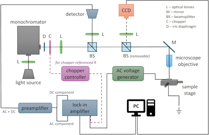
Figure 1: Schematic diagram of the experimental setup. Pink section only for chopper-referenced reflectance measurements with better signal-to-noise ratio. Please click here to view a larger version of this figure.
- Integrate the electronic chain by adding a low-noise current preamplifier between the photodiode and the lock-in amplifier. Route the AC component and the DC component of the detected signal to the lock-in amplifier.
- Connect a function/AC voltage generator to the piezoceramic element through insulated leads. Route the chopper reference output to the lock-in for reflectance measurements.
- Develop a control and acquisition application (e.g., LabVIEW) that communicates with the monochromator and the lock-in amplifier, reads the detector signal, and writes the results to a text file. Configure instrument drivers and communication ports on the host computer. See Figure 2 for an application block diagram example.
- Connect the lock-in output to a computer for data logging. After the optical alignment has been completed, the experiment can be paused with the system powered down.
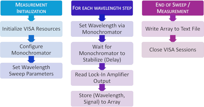
Figure 2: Software workflow for monochromator lock-in control and data acquisition. Block diagram of the control program (e.g., LabVIEW). Please click here to view a larger version of this figure.
NOTE: The control/acquisition application is hardware dependent. Because valid setups vary in instrument models and wiring, a specific LabVIEW code example is not portable and is therefore not provided. For a representative screenshot, see Supplementary Figure 1.
2. Preparation of the sample
NOTE: See Figure 3 for necessary equipment.
- Thin the bulk material to be characterized (e.g., a van der Waals crystal such as MoSe₂, MoS₂, WSe₂, WS₂) by repeated cleavage using adhesive tape (Figure 4A) until the preferred thickness is reached.
- Transfer the thinned fragments from the tape to a PDMS stamp by laminating PDMS onto the tape (Figure 4B) and peeling the PDMS back after ~5 min. so that flakes remain on the PDMS (Figure 4C) for subsequent transfer to the piezoceramic.
- Clean the piezoceramic surface by rinsing with acetone in a certified chemical fume hood. Dry the surface with clean, dry air or nitrogen.
CAUTION: Acetone is highly flammable and volatile; avoid ignition sources, avoid inhalation and skin/eye contact, and collect waste in approved containers inside a fume hood. Wear appropriate PPE (lab coat, safety glasses, and chemical-resistant gloves). - Apply a very thin layer of an adhesive medium to the piezoceramic (Figure 4D) (e.g., colorless nail polish as a thin adhesive, or a superglue layer for thicker films). Handle volatile adhesives in a chemical fume hood and allow a minimal amount to remain before transfer. Proceed promptly to the next step of the protocol to prevent the thin layer of adhesive from drying.
CAUTION: Many adhesives contain flammable solvents; handle inside a certified chemical fume hood and keep away from ignition sources. - Place the PDMS carrying the flake onto the wet adhesive on the piezoceramic, press gently to ensure contact (Figure 4E), wait ~30 s and remove (peel) the PDMS so that the material remains on the piezoceramic (Figure 4F). Verify adhesion by visual inspection (by eye); if needed or preferred, confirm under an optical microscope.
NOTE: Avoid lateral sliding of the PDMS stamp during contact to prevent tearing/dragging of flakes; peel the PDMS back smoothly.
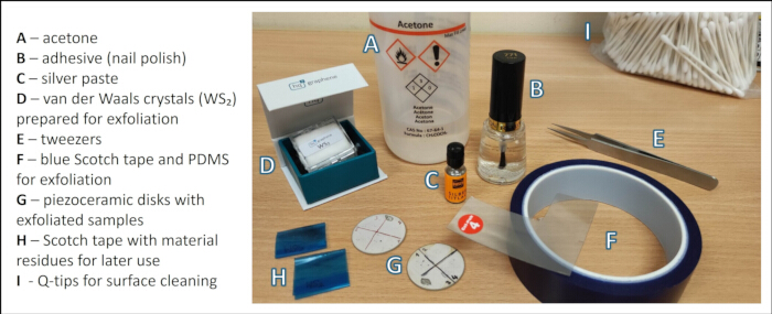
Figure 3: Materials for exfoliation and transfer to the piezoceramic. Please click here to view a larger version of this figure.
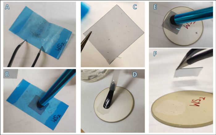
Figure 4. Step-by-step preparation and transfer of exfoliated vdW flakes onto a piezoceramic actuator. (A) Thickness reduction of the bulk crystal by repeated cleavage using adhesive tape. (B) Lamination of a PDMS stamp onto the tape to pick up thinned fragments. (C) Peeling the PDMS stamp using tweezers; exfoliated flakes are visible on the PDMS by eye (depending on thickness). (D) Application of a thin adhesive layer onto the piezoceramic surface to promote flake adhesion and strain transfer. (E) Placement of the PDMS stamp carrying flakes onto the wet adhesive layer for transfer. (F) Final piezoceramic actuator with flakes adhered to after PDMS removal, ready for optical alignment and piezoreflectance measurements. Please click here to view a larger version of this figure.
3. Sample mounting and connection
- Create separate electrodes to enable the application of an AC voltage across the piezoceramic.
- Place the piezoceramic with the transferred sample on the sample stage and secure it mechanically with silver paste, ensuring electric contact with the bottom electrodes of the piezoceramic.
- Form the top electrical contact using silver paste and copper wire. Allow the silver paste to fully dry (~10 h at room temperature) before applying any voltage to prevent contact damage.
CAUTION: Silver paste is highly toxic to aquatic organisms, causing long-term adverse effects. May cause drowsiness or dizziness. Flammable liquid and vapor.
- After applying the silver paste, cure at room temperature for approximately 10 h before proceeding. The prepared sample can be safely stored as long as the contacts are intact and conduct electricity.
- Insert the mounted sample into the optical setup. Connect the electrodes with insulated wires (Figure 5) to the AC voltage generator and to the ground. Keep all exposed conductors insulated and protected, away from the optical path.
CAUTION: High voltage may be present (e.g., up to 1500 V AC); use insulated leads, verify proper grounding, and do not touch live contacts. Enclose connections or use interlocks where available.
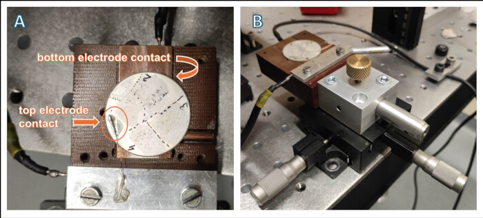
Figure 5: Piezoceramic disk actuator and sample-stage mounting for optical alignment. (A) Top view of the piezoceramic disk (Ø30 mm) with samples glued on its surface; leads are connected to the top (visible) and bottom (hidden under the piezoceramic disk) electrodes. (B) Actuator mounted on a manual X–Y translation stage with micrometer drives, enabling micrometric-precision positioning for optical alignment. Please click here to view a larger version of this figure.
4. Measurement of lock-in AC component proportional to ΔR and the DC component proportional to R
- Turn on the halogen light source and set it to maximum output. Ensure that the optical chopper is not obstructing the monochromator entrance slit.
- Power on the monochromator, preamplifier, lock-in amplifier, CCD camera, and control computer with the developed control and acquisition application. Wait at least 10 min until the system stabilizes. Among other things, stabilization of the signal depends on the heating due to turning on the halogen lamp.
- Set the monochromator to zero wavelength so that the entire lamp spectrum passes through. Select the diffraction grating/groove density appropriate for the measurement.
- Set the preferred width of the monochromator’s entrance/exit slit to achieve the desired spectral resolution.
NOTE: The narrower the slit, the better the spectral resolution of the measurement; however, less light reaches the sample, and the detected signal becomes weaker. The parameters should be adjusted experimentally to achieve the optimal effect. - Route the beam to the CCD camera and align the spot in the selected region of the sample using the XYZ microcontrollers. Adjust the iris diaphragm aperture to set the spot diameter on the sample.
- Switch the signal path from the CCD preview to the silicon PIN photodiode detector.
- Configure the preamplifier: set the bias voltage, filter type/cutoff, input offset, gain mode, and sensitivity to achieve a stable signal without saturation. Document the chosen values. For sample settings, see Supplementary Figure 2.
- Configure the lock-in amplifier to display X (in-phase). Set the reference frequency (e.g., 280 Hz) as intended for the AC voltage generator frequency and select the internal reference source. Then choose an appropriate time constant (typically ≥ 1 s; up to ~30 s for weak signals) and sensitivity. For sample settings, see Supplementary Figure 3A.
NOTE: Optimize the time constant and sensitivity empirically based on material response and available light, starting from values previously successful for similar samples. The time interval (delay) between measurement points should be longer than the time constant set during the measurement. - Enable the AC voltage generator and set the desired amplitude (e.g., 100 V). Verify that the signal reaches the piezoceramic without overdriving the device. For sample settings, see Supplementary Figure 4B. The frequency of the generated voltage is referenced from the lock-in amplifier. Verify the output is disabled before changing leads; enable output only after securing all electrical connections.
- Launch the acquisition application and select the measurement channel corresponding to the X lock-in output. Enter hardware-consistent parameters (time constant and sampling rate) and specify the output text file path for saving the data.
- Define the spectral range (wavelength or photon energy) and the monochromator step size according to instrument limits.
NOTE: Ideally, a sufficiently wide range is desired so that the spectrum baseline reaches zero outside the range of expected optical transitions. Remember that the spectral resolution of the measurements depends on the monochromator’s slit width. - Start the scan and allow it to continue uninterrupted until the end of the programmed range. Estimate the total duration as (number of steps) x (time constant) and plan accordingly. Do not interrupt the scan once it has started; continuous acquisition is required for consistent lock-in filtering.
- After completion, turn off the AC voltage generator without disturbing the position of the sample. Proceed with the reflectance (R) measurement.
5. Measurement of additional DC reflectance component (R) using chopper-referenced lock-in mode
- Confirm that the AC voltage generator remains off.
- Do not alter the beam position on the sample. If focus is uncertain, send the beam to the CCD preview, refocus and re-center the spot, and then return the signal path to the photodiode.
- Start the optical chopper with its controller and set its frequency equal to the modulation frequency used previously (e.g., 280 Hz). Verify that the chopper reference output is connected to the lock-in reference input. For sample settings, see Supplementary Figure 4A.
- Keep the preamplifier settings unchanged. In the lock-in amplifier, select the R (referenced reflectance) display, choose the chopper controller as the external reference source, and set input parameters identical to Section 4. Adjust the time constant (e.g., 0.1 s to 0.3 s typical) and the sensitivity to maintain a stable signal. For sample settings, see Supplementary Figure 3B.
NOTE: Expect shorter time constants and a larger signal value for R compared to ΔR. - In the acquisition application, select the lock-in R channel and mirror the lock-in time-constant setting. Set a new path for the output text file. Name files to encode the sample, the location on the sample, and the acquisition parameters so that the data sets of Section 4 (ΔR) and Section 5 (R) can be matched as pairs.
- Set the same spectral range and monochromator step size as used in Section 4 for the same spot on the sample. Start the scan and run it to completion.
- After completion, turn off the chopper. If no further measurements are planned the same day, turn off the light source, monochromator, and other instruments.
6. Analysis of the piezoreflectance spectrum (ΔR/R)
- Open the two text files collected in Section 4 and Section 5 in data-analysis software capable of plotting and data manipulation (e.g., OriginLab).
- Label the datasets for clarity (e.g., PzR for ΔR from Section 4 and R for reflectance from Section 5). Plot the PzR signal versus the photon energy or wavelength on appropriate axes; prefer the photon energy (eV) on the x-axis.
- If the PzR baseline deviates from zero outside expected transitions, perform a straight-line or baseline subtraction to zero the off-resonant regions. Document the operation parameters used.
- Compute ΔR/R by dividing the baseline-corrected PzR data by the R data point-by-point. Save the resulting ΔR/R as a new dataset.
- Plot ΔR/R versus photon energy to visualize resonances at optical transitions. Inspect the spectrum for features consistent with known transitions of the material.
- Fit ΔR/R using the Aspnes line-shape formalism12 (Equation 1) to extract transition energies and broadenings. Report the fit parameters and uncertainties.

Where y0 – baseline level (the flat line of the spectrum near the resonance), a, b – optional linear/quadratic baseline terms to absorb slow drift/curvature (use only if needed), θ – resonance phase, Eg – transition energy (peak position), Γ – linewidth/transition broadening, C – resonance amplitude, m – critical-point exponent, j – transition index.
NOTE: For discrete excitonic features, use m = 2; for interband critical points, use m = 2.5 or m = 3. In our practice, at low temperature we usually set m = 2; for T > 100 K, we set m = 2.5. This parameter also depends on the studied material.- Select the resonance window. Mark a fitting range that cleanly brackets the feature and contains short off-resonant segments on both sides.
- Enter strong initial guesses of the fit parameters. In the fit dialog, pre-fill the parameters you can read off, e.g., Eg – from the x-axis extremum; y0 – from the local baseline on the y-axis; C – from the peak-to-peak amplitude; m – per the rule above; a, b – set as zero, unlock only if needed for correcting fit line shape. Lock all parameters except for y0.
- Iteratively unlock the fitting parameters (one at a time):
Unlock C → fit
Unlock θ → fit
Unlock Γ → fit
Unlock Eg → fit
This will result in the final fine alignment. Only if residual slope/curvature remains, unlock a then b; otherwise, keep a = b = 0.
NOTE: Bounds that stabilize convergence: Γ ∈ [5, 300] meV; θ ∈ [−π, π]; C > 0; Eg within ± 50 meV of the visual extremum; y0 within ± 2× the off-resonant root mean square (RMS); keep ∣a∣ and ∣b∣ small (baseline only). - Accept the fit when: residuals are structureless around zero inside the window; parameters change by <1% upon a small change of the window; and refitting from perturbed seeds returns the same solution.
- Calculate the modulus for each direct transition using Equation 2.
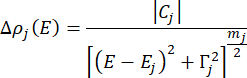
NOTE: The index j labels each individual critical point/transition included in the model (e.g., j = 1 for the A exciton, j = 2 for the B exciton, j = 3 for a higher-energy interband feature, etc.). Each j has its own fitted parameters (Ej, Γj, mj, Cj, θj); only the modulus |Cj∣ enters Equation 2, so Δρj is phase-independent.- Compute Δρj(E) for each fitted transition with parameters (Ej, Γj, mj, Cj) taken from the Aspnes (TDFF) fit (Section 6.6). Plot Δρj(E) (and, if needed, the total Δρ(E) = ∑jΔρj(E)) to compare the transition strengths between samples or conditions.
Access restricted. Please log in or start a trial to view this content.
Results
Lock-in piezoreflectance (PzR) yields derivative-like signatures at direct optical transitions across a broad set of van der Waals (vdW) crystals and semiconductor microstructures. Figure 6 shows typical raw output from a single spot in WS₂ acquired with the workflow in Sections 4–6: strain-modulated AC reflectance ΔR, reference DC component proportional to reflectance R (Figure 6A), and the baseline-corrected ratio ΔR/R (Figure 6B). With a piezoceramic disk...
Access restricted. Please log in or start a trial to view this content.
Discussion
Here we present piezoreflectance (PzR) spectroscopy for van der Waals crystals, a protocol that uses periodic strain from a piezoceramic transducer to produce derivative-like reflectance spectra and isolate critical points with high contrast. Compared with reflectance contrast (RC), the method sharpens weak or overlapping resonances and extends to cases where RC provides ambiguous contrast, while retaining a single broadband optical path and compatibility from monolayers to bulk; the primary tradeoffs are the lack of abs...
Access restricted. Please log in or start a trial to view this content.
Disclosures
The authors have nothing to disclose.
Acknowledgements
This study was supported by a grant from the Polish National Science Center (PRELUDIUM BIS 4 ,
Project No. 2022/47/O/ST3/01965).
Access restricted. Please log in or start a trial to view this content.
Materials
| Name | Company | Catalog Number | Comments |
|---|---|---|---|
| Acetone (analytical grade) | Sigma-Aldrich / Merck | 650501 | |
| CCD Camera | e.g. Hamamatsu Photonics / Princeton Instruments / Thorlabs | N/A | |
| Computer with control and data acquisition software (e.g., LabVIEW) | National Instruments / Custom setup | N/A | |
| DSP Lock-In Amplifier | Stanford Research Systems (SRS) | SR810 | |
| EKE Halogen Lamp, 150 W 21 V (GX5.3 base) | OSRAM | 93638 | Used as the replacement bulb for the Thorlabs OSL1-EC Fiber Illuminator. |
| Gel-Film PDMS-based viscoelastic film, 4.0″×4.0″ sheet | Gel-Pak | WF-40×40-0060-X4 | |
| High Intensity Fiber Light Source (halogen lamp) - 150 W | Thorlabs | OSL1-EC | The model is listed as discontinued (superseded by OSL2) as of 07 Jan 2014. |
| High Voltage Rectangular Signal Generator | Custom-made in our laboratory | HVG-3 | |
| Low-Noise Current Preamplifier | Stanford Research Systems (SRS) | SR570 | |
| M Plan APO NIR 50× Objective Lens | Mitutoyo Corporation | 378-825-17 | Other objectives with suitable magnification and spectral transmission can also be used depending on the optical setup. |
| Monochromator / Imaging Spectrograph, focal length 320 mm - Zolix Omni-λ300i | Zolix Instruments Co., Ltd. | Omni-λ300i | |
| Optical Chopper Controller | Stanford Research Systems (SRS) | SR540 | |
| Optomechanical and optical components (lenses, mirrors, irises, optical chopper, beam splitters, optical fibers, and mounts) | Thorlabs / custom-made | Various | |
| Piezoelectric Ceramic Disk (Ø30 × 1 mm, PZT-5O, silver electrodes) | He-Shuai Ltd. | N/A | |
| PVC Surface Protection Low-Adhesion Cleanroom Tape (blue) | Cleanroom Supply | N/A | |
| Silicon PIN Photodiode | e.g. Hamamatsu Photonics / Thorlabs | N/A | Other types of photodetectors can be employed depending on the spectral range of interest. |
| Silver conductive varnish (“Leitlack”) | Busch GmbH & Co. KG | 5900 | |
| Transparent nail polish | Revlon, Inc. | N/A | Used as an adhesive layer for fixing vdW flakes. Any clear nail polish of similar composition can be used as an alternative. |
| Tungsten Disulfide (WS2), CAS 12138-09-9 | HQ Graphene | N/A | sample material |
References
- Gavini, A., Cardona, M. Modulated piezoreflectance in semiconductors. Phys Rev B. 1, 672(1970).
- Dumcenco, D. O., et al. Piezoreflectance and Raman Characterization of Mo1−xWxS2 Layered Mixed Crystals. Solid State Phenomena. 170, 55-59 (2011).
- Zheng, J. Y., Lin, D. Y., Huang, Y. S. Piezoreflectance study of band-edge excitons of res2:au. Jpn J Appl Phys. 48, 0523021-0523025 (2009).
- Wu, Y. J., et al. Piezoreflectance study of near band edge excitonic-transitions of mixed-layered crystal Mo(SxSe1-x)2 solid solutions. J Appl Phys. 115, 223508(2014).
- Sigiro, M., Huang, Y. S., Ho, C. H., Lin, Y. C., Suenaga, K. Influence of rhenium on the structural and optical properties of molybdenum disulfide. Jpn J Appl Phys. 54, 04DH05(2015).
- Kopaczek, J., et al. Direct optical transitions at K- and H-point of Brillouin zone in bulk MoS2, MoSe2, WS2, and WSe2. J Appl Phys. 119, 235705(2016).
- Kopaczek, J., et al. Strain Modulation in van der Waals Crystals Directly Exfoliated onto Piezoceramics─Application in Micropiezoreflectance Spectroscopy. ACS Appl Electron Mater. 6, 7857-7864 (2024).
- Ruppert, C., Aslan, O. B., Heinz, T. F. Optical Properties and Band Gap of Single-and Few-Layer MoTe2 Crystals. Nano Lett. 14, 6231-6236 (2014).
- Niu, Y., et al. Thickness-Dependent Differential Reflectance Spectra of Monolayer and Few-Layer MoS2, MoSe2, WS2 and WSe2. Nanomaterials. 8, 725(2018).
- CARDONA, M. Optical Properties and Electronic Density of States. J Res Natl Bur Stand A Phys Chem. 74A, 253(1970).
- Misiewicz, J., Sitarek, P., Sęk, G., Kudrawiec, R. Semiconductor heterostructures and device structures investigated by photoreflectance spectroscopy. Mater Sci. 21 (3), 263-318 (2003).
- Aspnes, D. E. Third-derivative modulation spectroscopy with low-field electroreflectance. Surf Sci. 37, 418-442 (1973).
- Misiewicz, J., Sęk, G., Sitarek, P. Photoreflectance spectroscopy applied to semiconductors and semiconductor heterostructures. Optica Appl. 29, 327-363 (1999).
- Aspnes, D. E. Analysis of modulation spectra of stratified media. JOSA. 63 (11), 1380-1390 (1973).
- Philipp, H. R., Dash, W. C., Ehrenreich, H. Piezoreflectance in Ge. Phys Rev. 127, 762-765 (1962).
- Pollak, F. H., Cardona, M. Piezo-Electroreflectance in Ge, GaAs, and Si. Phys Rev. 172, 816(1968).
- Merski, J., Eckhardt, C. J. Piezomodulation spectroscopy of molecular crystals. I. Methods and principles. J Chem Phys. 75, 3691-3704 (1981).
- Mathieu, H., Allègre, J., Gil, B. Piezomodulation spectroscopy: A powerful investigation tool of heterostructures. Phys Rev B. 43, 2218(1991).
- Yu, C. H., et al. Multiple confined-state transitions within surface quantum dots by a piezomodulation reflectance study. Phys Status Solidi (A) Appl Mater Sci. 204, 1171-1177 (2007).
- Engeler, W. E., Fritzsche, H., Garfinkel, M., Tiemann, J. J. High-Sensitivity Piezoreflectivity. Phys Rev Lett. 14, 1069(1965).
- Garfinkel, M., Tiemann, J. J., Engeler, W. E. Piezoreflectivity of the Noble Metals. Phys Rev. 148, 695(1966).
- Sell, D. D., Kane, E. O. Piezoreflectance of Germanium from 1.9 to 2.8 eV. Phys Rev. 185, 1103(1969).
- Gerhardt, U., Beaglehole, D., Sandrock, R. Piezo-Optical Constants, Deformation Potentials, and the Electronic Structure of Copper. Phys Rev Lett. 19, 309(1967).
- Balslev, I. Apparatus for Combined Static and Dynamic Uniaxial Stress. Rev Sci Inst. 38, 1528-1529 (1967).
- Sell, D. D. Review of piezomodulation spectroscopy. Surf Sci. 37, 896-913 (1973).
- Sebayang, K., Sigiro, M. Piezoreflectance study of Nb-doped MoS2 single crystals. IOP Conf Seri Mater Sci Eng. , Institute of Physics Publishing. (2017).
- Kopaczek, J., et al. Experimental and Theoretical Studies of the Electronic Band Structure of Bulk and Atomically Thin Mo1- xW xSe2Alloys. ACS Omega. 6, 19893-19900 (2021).
- Gerhardt, U. Piezoreflectance in Si. Phys Lett. 9, 117-118 (1964).
- Kopaczek, J., et al. Temperature Dependence of the Indirect Gap and the Direct Optical Transitions at the High-Symmetry Point of the Brillouin Zone and Band Nesting in MoS2, MoSe2, MoTe2, WS2, and WSe2Crystals. J Phys Chem C. 126, 5665-5674 (2022).
- Kudrawiec, R., Misiewicz, J. Photoreflectance and contactless electroreflectance measurements of semiconductor structures by using bright and dark configurations. Rev Sci Instrum. 80, 096103(2009).
- Piezoceramic Materials. , PI Ceramic GmbH. https://www.piceramic.com/en/expertise/piezo-technology/piezoelectric-materials (2026).
Access restricted. Please log in or start a trial to view this content.
Reprints and Permissions
