This protocol presents a high-throughput process for the fabrication and characterization of perovskite thin-film field effect transistors. We describe a customizable fabrication process using photolithography and present an automated characterization procedure combining a multiplexer with custom measurement boards and self-written software.
Method Article
Enabling High-Throughput Perovskite FET Research by a Customizable Automated FET Measurement Station
In This Article
Summary
Abstract
Perovskite-based thin-film field effect transistors (PeFETs) have yet to achieve the full theoretical potential of this promising class of materials. To bridge this gap, it is essential to develop and optimize novel perovskite compositions and fabrication techniques. Given the large variety of potential compounds as well as the manifold of influencing variables such as concentration, temperature, and choice of solvent, a high-throughput research approach is critical for efficient exploration and advancement. We present a flexible and customizable process that spans from substrate fabrication to device characterization. This process is enabled by and integrates photolithography for custom patterning, an automated measurement station for FET characterization, and automated data analysis. The automated measurement station is based on a multiplexer, which is connected to five measurement boards. The measurement boards are configured to measure one substrate with four devices each. Allowing the automated measurement of 20 devices with up to 5 different perovskite formulations. Using standardized testing procedures, the raw data is automatically analyzed to get the transfer and output characteristics of the PeFETs as well as key performance parameters like the threshold voltage, subthreshold swing, and the field effect mobility. The result is a systematically organized data pool with easily comparable data for different perovskite compositions or modifications in fabrication conditions.
Introduction
The field of metal halide perovskite (MHP) based optoelectronic devices has seen an astonishing progress over the last two decades. Especially the successful incorporation into photovoltaics and light-emitting diodes (LEDs) has led to an ever-increasing interest in this material class. The power conversion efficiency of MHP-based solar cells has rapidly increased from 13.9% in 2013 to 26.7% in 20241,2,3,4,5,6. MHP-based LEDs have exceeded an external quantum efficiency of 20% over a wide range of the visible spectrum, utilizing the ability of a fine-tunable band gap, also enabling dual color LEDs7,8,9. These impressive developments show the capabilities of MHPs for optoelectronic devices.
Nevertheless, the progress in the field of MHP-based thin-film field effect transistors (PeFETs) has not yet seen the same success in development. Despite the fact, that the theoretical properties of MHPs should make them a promising choice for FETs, with theoretical charge carrier mobilities of over 1000 cm2V-1s-1 and long-range balanced carrier transport10,11,12. However, the highest performance real-world devices have reached charge carrier mobilities of up to 55 cm2V-1s-1, which is already an impressive achievement, but it shows that there is still a lot of room for improvement13.
The increasing performance of PeFETs over the past few years was achieved by optimizing the device architecture, interface properties, and MHP composition13,14,15,16. Furthermore, the addition of a variety of additives like SnF2, SbF3, or pseudohalides has shown promising results17,18,19,20. The combination of the large number of possible perovskite precursors with the increasing number of interesting additives leads to a very high number of possible perovskite compositions. Taking the variety of experimental variables, like concentration, solvent, and temperature, into consideration, a high-throughput method is essential in the search for high-performance PeFETs.
We present a scalable and customizable fabrication process for transistor substrates that is based on photolithography. Most of the used PeFET architectures rely on at least one of the contact layers on a shadow mask system17,18,19,20,21. While being simple to use and very time efficient, shadow masks have relatively soft edges and wear out over time. Furthermore, the pattern is predefined and cannot be adapted to changing requirements. Photolithography, in contrast, has very sharply defined patterns and edges because the photoresist is applied directly to the surface of the substrate. With maskless photolithography, the pattern can be changed for every exposure if necessary, enabling batch-to-batch or even substrate-to-substrate adjustments. Because the exposure of single substrates is tedious and time-consuming, a 5 cm x 5 cm glass substrate is processed as one unit up to the point at which all the electrodes are finished and is then diced into 25 1 cm x 1 cm substrates, drastically reducing the fabrication time from 16 h to 4 h. It is also possible to use a larger glass substrate, which will increase the number of substrates per batch and scale up the process.
To take advantage of the increase in fabrication speed, it is also essential to have a characterization process that can reliably work with a large number of devices. We present a measurement setup, that combines a multiplexer with self-made measurement boards, which can be controlled directly from the control software of the parameter analyzer (Figure 1). This setup enables the automatic measurement of 5 substrates with 4 devices each. After the measurement, the resulting data is automatically evaluated by a self-written script (Supplementary File 1), which calculates key performance parameters of PeFETs and saves them to a data pool, making it easy to compare the results and see long-term trends.
Combining the faster fabrication process with the automated characterization procedure enables a reliable, scalable, and high-throughput process that is also flexible and customizable, making it a strong tool in the search for new MHP compositions.

Figure 1: Experimental schematic of the presented high-throughput PeFETs research process. (1) The substrate fabrication on a single large substrate. (2) The processing of the single substrate by applying the perovskite. (3) The automated measurement and data analysis. Please click here to view a larger version of this figure.
Protocol
The details of the reagents and the equipment used in this study are listed in the Table of Materials.
1. Photolithography
- Substrate cleaning
- Take a 50 mm by 50 mm glass substrate and sonicate it for 10 min in Isopropanol (IPA), followed by drying with a nitrogen gun. Repeat with acetone.
- After drying, place the substrate in a low-pressure oxygen plasma (5 min, 20 sccm, 0.35 mbar, 150 W).
NOTE: This procedure is the standard cleaning procedure and is meant to be repeated whenever the following text says clean substrates.
- Gate lithography
- Place the cleaned substrate on a spin coater and pipette 600 µL photoresist onto the middle of the substrate. Start the spin coater (60 s, 4000 rpm, 2000 acc, 3.5 µm).
- Transfer the substrate onto a preheated hot plate for pre-exposure baking (60s, 110 °C). After cooling down, transfer the substrate to the maskless photolithography machine for exposure (15 mW, 75%, 1 x 1).
- Place the fully exposed substrate on a preheated hot plate for post-exposure baking (70 s, 110 °C).
- Develop the photoresist in the developer for 90 s, rinse with water, and dry with a nitrogen gun.
- Gate Cu evaporation
- Transfer the substrate to a low-pressure oxygen plasma (5 min, 20 sccm, 0.35 mbar, 150 W).
- Place the substrate in an evaporation chamber. Firstly, evaporate 5 nm Cr, followed by 50 nm Cu. Take the substrate out of the evaporation chamber, submerge it in the remover and sonicate for 30 min at 50 °C.
- Atomic layer deposition (ALD) of Al2O3
- Clean the substrate. Transfer the substrate into the ALD machine. Run the Al2O3 recipe for 800 cycles, resulting in a 100 nm layer of Al2O3.
NOTE: One cycle consists of a 35-ms trimethylaluminium followed by a 250-ms H2O pulse. The chamber temperature for the first 25 cycles is 100 °C, and for the following 775 cycles, 200 °C.
- Clean the substrate. Transfer the substrate into the ALD machine. Run the Al2O3 recipe for 800 cycles, resulting in a 100 nm layer of Al2O3.
- Source/drain lithography
- Clean the substrate. Apply photoresist to the substrate as described in step 1.2.
- Align the substrate with the markers from the first lithography layer in the photolithography machine before exposure. Expose, post-exposure bake, and develop following step 1.2.
- Source/drain Au evaporation
- Transfer the substrate to a low-pressure oxygen plasma (5 min, 20 sccm, 0.35 mbar, 150 W). Place the substrate into an evaporation chamber. Firstly, evaporate 5 nm Cr, followed by 50 nm Au.
- Remove the substrate from the evaporation chamber, submerge it in photoresist stripper, and sonicate for 30 min at 50 °C.
- Dicing the substrate
- Clean the substrate. Apply photoresist using the spin coater (60 s, 4000 rpm, 2000 acc, 3.5 µm). Place the substrate on a hot plate (5 min, 110 °C).
- Transfer the substrate to the wafer saw and dice it into 10 mm x 10 mm substrates. Remove the photoresist by sonicating for 30 min at 50 °C in the remover (Figure 2).
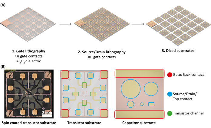
Figure 2: Schematic representation of the 5 cm x 5 cm substrate fabrication process. This includes subsequent photo lithography steps, followed by dicing to 1 cm x 1 cm substrates (A). Images of the final transistor substrates containing 4 devices with and without a perovskite layer and of a capacitor substrate (B). One capacitor substrate per batch is fabricated to measure the dielectric constant of the Al2O3 layer. Please click here to view a larger version of this figure.
2. Spin coating the perovskite layer
NOTE: From here on, all the following steps are carried out in a glovebox due to the air sensitivity of the perovskite layer.
- Solution preparation
- Prepare the precursor solution 1 day ahead of spin coating.
- Weigh in 150 mg SnI2 and dissolve in 1398 µL DMF. Weigh in 125 mg CsI and dissolve in 1203 µL of the SnI2 solution. Weigh in 15 mg PbI2 and dissolve in 1017 µL of the CsSnI3 solution, resulting in a 0.4 M solution of Cs(Sn0.9Pb0.1)I3 with an excess of Cs in relation to Sn + Pb of 1.25:1. Weigh in 6 mg of SnF2 and dissolve in 1000 µL DMF.
- Shake the prepared solutions at 60 °C overnight.
- Spin coating
- Add 765 µL of the prepared SnF2 solution to the 1017 µL Cs(Sn0.9Pb0.1)I3 solution right before spin coating. Place the substrate in the spin coater.
- Pipette 20 µL of the prepared precursor solution in the middle of the substrate. Start the spin coater (150 s, 4000 rpm, 1000 acc, 40 nm). Anneal the spin-coated substrates for 5 min at 120 °C.
- Separating the devices
- On each substrate are four devices, which need to be separated to prevent cross-interaction. Take a cotton stick, dip it in DMF and take a substrate of the hot plate.
- Draw with the cotton stick on the still-hot substrate around the single devices and separate the perovskite layer. Remove the perovskite layer from all the contact pads in the same way.
3. Characterization
- Hardware setup
- Place the substrate upside down in the measurement board and make sure the contact pads of the right devices align with the corresponding pins on the measurement board (Figure 3).
- Connect the measurement board with the multiplexer. Connect the multiplexer to the SMU of the parameter analyzer via two coaxial cables, one for the gate contact and one for the source/drain contacts, which connect the source to the SMU and the drain to ground.
- Software setup
- Ensure all cables are connected in the right way. Turn on the parameter analyzer and start the control software as an administrator.
- Configure the measurement by defining how many measurement boards are connected to the multiplexer and loaded with a substrate. Define the names/identifiers for the substrates and the number of devices that are supposed to be characterized.
- Configure the drain for all measurements as a common ground. For transfer measurements, configure a voltage linear sweep at the gate ranging from 25 V to -30 V, with a voltage step of -0.1 V. Configure the source as constant bias with 1 V, 10 V, and 30 V, respectively.
- For the output measurements, configure voltage steps at the gate ranging from -30 V to 10 V, with a step size of 10 V.
- Configure a voltage linear sweep at the source ranging from 0 V to -30 V, with a step size of 0.5 V. Before starting the measurement, set the source and gate current range to limited auto with a limit of 1 nA.
- Measurement
- Hit Run on the software interface, and the measurement will start. The multiplexer switches through the predefined devices, and the parameter analyzer carries out the configured tests.
NOTE: When the measurement finishes, the data can be reviewed directly in the control software of the parameter analyzer and can be exported as xlsx-files.
- Hit Run on the software interface, and the measurement will start. The multiplexer switches through the predefined devices, and the parameter analyzer carries out the configured tests.
- Data export
- Export the measurement data as xlsx-files. The file name must contain the batch number as well as the substrate numbers and the source-drain bias for the transfer measurements.
NOTE: For example, if the substrates 1 to 5 of the first batch were measured, the output data file is named "Batch1_S1_S2_S3_S4_S5_Output.xlsx". This means that substrate 1 was placed in the first measurement board, substrate 2 in the second measurement board, and so on. The corresponding transfer data-file is named "Batch1_S1_S2_S3_S4_S5_Transfer_10V.xlsx", if the transfer was measured at a source-drain bias of 10 V. There is also a log-file in the file explorer, that contains information about which data corresponds to which device.
- Export the measurement data as xlsx-files. The file name must contain the batch number as well as the substrate numbers and the source-drain bias for the transfer measurements.

Figure 3: 3D model of the measurement board setup. (A) Visualization of placing a substrate in the measurement board. (B) Pin array on the measurement board with and without a loaded substrate. Please click here to view a larger version of this figure.
4. Data analysis
- Automated data analysis
- Transfer the xlsx data file and the log file to the desired computer and place the files in the "Data" folder. Run the Python script Auto_Data_analysis.py (Supplementary File 1).
NOTE: The script asks for the identifiers of the substrates and if multiple transfer measurements were taken at different source/drain voltages. If multiple transfer measurements were taken, the script asks for the values of the source/drain voltages. After all the necessary information is entered, the script runs through the data and creates a folder named "Plots". Enter the "Plots" folder, which contains two folders, "Short" and "Working". The "Short" folder contains the plots of devices that did not function properly, and the "Working" folder contains the plots of the working devices. Enter the "Working" folder, inside are PNG files that are named after the corresponding devices and show an overview of all the output and transfer plots, as well as the measurement configuration and calculated performance parameters.
- Transfer the xlsx data file and the log file to the desired computer and place the files in the "Data" folder. Run the Python script Auto_Data_analysis.py (Supplementary File 1).
- Data pool
- Ensure that the Python script also creates one text file for every batch and one combined text file for all devices, which contains metadata like experimental variables and performance parameters, and can be used to analyze the data with any separate data analysis software.
Results
To validate the fabrication method for the bottom gate and bottom contact substrates and ensure that the whole stack of the architecture functions properly after the subsequent lithography steps and dicing of the large glass substrate, all devices go through quality control. After dicing and before the perovskite layer is applied, all substrates of the batch are placed in the measurement setup. Between the source and drain contacts, 10 V is applied, and the gate is swept from -40 V to 30 V. The test range is chosen according to the range of interest for the PeFETs for which the substrates will be used. The maximum current that is measured at the gate contact is recorded and evaluated. Any device with a maximum gate current smaller than 1 x 10⁻⁷ A is considered good under these test conditions. Figure 4 shows an example of such quality control. Only 6 out of the 96 devices fail the quality control, with 2 of the 6 being completely short. The high yield of functioning devices shows that the device architecture is stable enough to withstand the stress of the dicing and ensures time savings compared to a process during which single substrates are processed.

Figure 4: Exemplary result of a quality control at the end of the substrate fabrication process. The matrix shows the maximum measured gate current in amperes during the quality control for 24 substrates of one batch, with 4 devices each. The green devices pass the quality control. In this example, 6 of the 96 devices failed the quality control. Please click here to view a larger version of this figure.
PeFETs based on a Cs(Sn0.9Pb0.1)I3 perovskite were fabricated and measured using the automated measurement setup. In the used setup, 5 measurement boards, with the capability to connect 4 PeFETs each, were connected to a multiplexer, which was connected to a parameter analyzer. Enabling the automated measurement of up to 20 PeFETs. The devices had a channel length of 150 µm and a channel width of 1 mm. Both the gate and source-drain contacts were fabricated using maskless photolithography, which allowed for precise control over the size of the gate electrode. By minimizing the gate contact area, the overlap between the perovskite layer and the gate is reduced. This lowers the likelihood of defects in the dielectric region between the perovskite and the gate, which could otherwise lead to short circuits. All measurements were carried out in a N2-filled glovebox. Using the data analysis script, a quick overview of the device key parameters is generated. Figure 5 displays a screenshot of the automatically generated plots of the transfer and output characteristics as described below. In this example, three different source/drain voltages were measured for the transfer characteristic (A, B, C), to obtain at least one measurement in the linear regime and one measurement in the saturation regime. The script analyzes the output characteristic first and extrapolates the linear and saturation regimes from a linear fit to the output curves (1). The linear regime is marked by the red background and the saturation regime by the blue background. Because there are multiple methods to determine the threshold voltage, which can lead to significantly different results for FETs with non-ideal properties, the script determines the threshold voltage in three different ways. The first threshold voltage is calculated from the output characteristic (1) by determining the border between the linear and saturation regime. The second threshold voltage is extrapolated by plotting the square root of the source/drain current versus the gate voltage (4) and linear fitting the saturation regime. The intersection of the linear fit with the x-axis determines the threshold voltage. Analogously, the threshold voltage in the saturation regime is determined by linear fitting the plot of the source/drain current versus the gate voltage (3) and determining the x-axis intersection. The charge carrier mobilities for the saturation and linear regime are calculated from the slopes of the corresponding linear fits. The last plot that is shown is the transfer characteristic on a logarithmic scale (2). In this plot, the point of the maximum slope is determined to calculate the subthreshold swing. The plots (1) and (3) also show the corresponding gate current on a second y-axis with an adapted range, which makes it easy to quickly see the non-ideal behavior of the gate current.
As shown in Figure 5, all the calculated performance parameters as well as the measurement settings, are collected in a table for each source/drain voltage. Furthermore, all the linear fits are shown in the plots, allowing for a quick check if the fits are sensible. For example, in the transfer plot on a logarithmic scale for -1 V (A2), the script clearly did not determine the real point of maximum slope and therefore is underestimating the subthreshold swing of the device. To find the point of maximum slope, the script first determines and cuts off the noisy part of the plot. Because the real point of maximum slope in this case is very close to the noisy part of the plot, the script falsely cuts it off, showing that further refinement of the script is necessary. Nevertheless, the script gives a fast and easy overview of the device performance and enables the comparison between different devices.
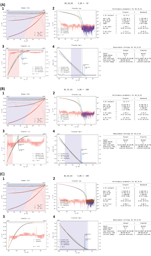
Figure 5: Automatically generated visual overview of the performance data of a PeFET. The Data for three different source/drain voltages during the transfer measurement is shown (A: -1 V, B: -10 V, C: -30 V). For every source/drain voltage, the output plot (1), transfer plot on a logarithmic scale (2), transfer plot on a linear scale (3), and the square root of the transfer plot on a linear scale (4) are shown. Plots (1) and (3) additionally display the corresponding gate current on a secondary y-axis with an appropriate range. This allows for a straightforward identification of non-ideal behavior in the gate current. The tables next to the plots are the extrapolated and calculated performance parameters and the measurement settings. Please click here to view a larger version of this figure.
Besides the visual overview that is shown in Figure 5, the performance parameters are additionally stored in a table form in a text file. The experimental data is also stored in such a file. This can be used to compare the data in any available data analysis software, which makes it easy to see performance trends over time or find connections between experimental variables and performance parameters.
Supplementary File 1: Python script forAuto_Data_analysis.py. Please click here to download this File.
Discussion
The presented high-throughput process for the fabrication and characterization of PeFETs provides a scalable and flexible approach to exploring novel perovskite compositions. By integrating photolithography for precise substrate fabrication with an automated measurement and data analysis, the method significantly enhances experimental efficiency13,14. One of the key advantages of this approach is the ability to rapidly generate and compare systematically structured datasets, which is crucial in the search for optimized PeFET performance15,16.
A critical step in this method is the photolithography-based fabrication of transistor substrates. Compared to traditional shadow mask methods, photolithography offers superior pattern definition and flexibility in device layout21. This advantage is particularly relevant in basic research, where minor modifications to device architecture may be required between batches or even within a single experimental iteration. Even though shadow mask methods are, in general, simpler and time efficient in relation to photolithography, these limitations can be overcome by starting with a large substrate, which gets diced in the end, reducing the number of lithography runs needed and reducing the fabrication time by 75% for 24 substrates. The quality control of the substrate after dicing validated the stability of the substrates to withstand the added stress13.
The integration of a multiplexer with custom measurement boards simplifies and accelerates the characterization process, enabling the evaluation of up to 20 devices with up to 5 different perovskite compositions in a single run13,17.
Finally, the automated data analysis ensures efficient processing and interpretation of experimental results. By systematically extracting key performance parameters such as charge carrier mobility, threshold voltage, and subthreshold swing, the method enables rapid comparison of different perovskite formulations and processing conditions. One challenge, however, lies in the sensitivity of the analysis script to non-ideal device behaviors. Despite these limitations, the presented methodology provides a powerful and flexible tool for gathering a wide range of performance metrics quickly, facilitating systematic optimization of materials and processing conditions with high efficiency19,20.
Disclosures
The authors have nothing to disclose.
Acknowledgements
This work was carried out in the framework of the Joint Lab GEN_FAB and with the support of the Helmholtz Innovation Lab HySPRINT.
Materials
| Name | Company | Catalog Number | Comments |
|---|---|---|---|
| µPG 101 | Heidelberg Instruments | photolithographer | |
| Acetone | Roth | 5025.2 | |
| AZ 2026 MIF | MicroChemicals | 1002026 | developer |
| AZ nLOF 2027 | MicroChemicals | 1A002070 | photoresist |
| CsI | TCI | C2205 | |
| DMF | Roth | T921.1 | |
| Femto plasma | Diener | low pressure plasma | |
| GEMStarXT | Arradiance | ALD | |
| Isopropanol | Roth | CN09.1 | |
| Keithley 4200A-SCS | Tektronix | parameter analyzer | |
| LabSpin6 | SUSS MicroTec | spin coater | |
| PbI2 | TCI | L0279 | |
| SnF2 | Thermo Scientific Chemicals | AC308600050 | |
| SnI2 | TCI | T3449 | |
| TechniStrip NI555 | MicroChemicals | TNI555M5 | lift off |
| Trimethylaluminium | Strem | 93-1360 |
References
- Pellet, N., et al. Mixed-organic-cation perovskite photovoltaics for enhanced solar-light harvesting. Angew Chem Int Ed. 53 (12), 3151-3157 (2014).
- Liu, C., et al. Bimolecularly passivated interface enables efficient and stable inverted perovskite solar cells. Science. 382 (6672), 810-815 (2023).
- Green, M. A., et al. Solar cell efficiency table (Version 63). Prog. Photovolt: Res. Appl. 32 (1), 3-13 (2024).
- Yoshikawa, K., et al. Silicon heterojunction solar cell with interdigitated back contacts for a photoconversion efficiency over 26%. Nat Energy. 2, 17032(2017).
- Best research-cell efficiencies. , NREL. accessed 01 https://www.nrel.gov/pv/cell-efficiency.html (2025).
- Xie, Z., et al. High-efficiency perovskite solar cells enabled by guanylation reaction for removing MACl residual and in situ forming 2D perovskite. Angew Chem Int Ed. 64 (7), e202419070(2025).
- Lin, K., et al. Perovskite light-emitting diodes with external quantum efficiency exceeding 20 percent. Nature. 562, 245-248 (2018).
- Zhang, K., Zhu, N., Zhang, M., Wang, L., Xing, J. Opportunities and challenges in perovskite LED commercialization. J. Mater. Chem. C. 9 (11), 3795-3799 (2021).
- Schröder, V. R. F., et al. large area, inkjet-printed metal halide perovskite light emitting diodes. Mater. Horiz. 11, 1989-1996 (2024).
- Kagan, C. R., Mitzi, D. B., Dimitrakopoulos, C. D. Organic-inorganic hybrid materials as semiconducting channels in thin-film field-effect transistors. Science. 286 (5441), 945-947 (1999).
- Yu, J. C., Park, J. H., Lee, S. Y., Song, M. H. Effect of perovskite film morphology on device performance of perovskite light-emitting diodes. Nanoscale. 11, 1505-1514 (2019).
- Chen, Q., et al. Under the spotlight: The organic-inorganic hybrid halide perovskite for optoelectronic applications. Nano Today. 10 (3), 355-396 (2015).
- Liu, A., et al. High-performance inorganic metal halide perovskite transistors. Nat Electron. 5, 78-83 (2022).
- Matsushima, T., et al. Solution-processed organic-inorganic perovskite field-effect transistors with high hole mobilities. Adv. Mater. 28 (46), 10275-10281 (2016).
- Senanayak, S. P., et al. Understanding charge transport in lead iodide perovskite thin-film field-effect transistors. Sci. Adv. 3 (1), e1601935(2017).
- Yusoff, A. R. bM., et al. Ambipolar triple cation perovskite field-effect transistors and inverters. Adv. Mater. 29 (8), 1602940(2017).
- Liu, A., et al. Antimony fluoride (SbF3): A potent hole suppressor for tin(II)-halide perovskite devices. InfoMat. 5 (1), e12386(2023).
- Cho, J. -H., et al. Anion-vacancy-defect passivation of a 2D-layered tin-based perovskite thin-film transistor with sulfur doping. Adv Electron Mater. 9 (3), 2201014(2023).
- Go, J. -Y., et al. A large bandgap organic salt dopant for Sn-based perovskite thin-film transistor. Adv Funct Mater. 33 (44), 2303759(2023).
- Park, G., et al. High-performance tin perovskite transistors through formate pseudohalide engineering. Mater Sci Eng R. 159, 100806(2024).
- Zhu, H., et al. Fabrication of high-performance tin halide perovskite thin-film transistors via chemical solution-based composition engineering. Nat Protoc. , 1-15 (2025).
Reprints and Permissions
This article has been published
Video Coming Soon