A unique method for preparing operando transmission electron microscopy (TEM) samples on micro-electromechanical systems (MEMS) chips is presented. Electrical contacts are deposited using a focused ion beam, with resistance minimized via on-chip heating, and evaluated across varying sample dimensions, enabling electrical conductivity measurements at different temperatures during in situ TEM observations.
Method Article
Sample Preparation and Resistivity Measurements for Operando Transmission Electron Microscopy During Heating and Electrical Biasing
Opens in a new tab
In This Article
Summary
Loading...
$$\rightleftharpoonup{xx}$$
$$\longleftharp{xx}$$,
$$\longrightharp{xx}$$,
Abstract
Loading...
$$\rightleftharpoonup{xx}$$
$$\longleftharp{xx}$$,
$$\longrightharp{xx}$$,
Characterizing microstructures of materials is essential for understanding the relationships with their properties. However, the microstructure can experience changes during operation at elevated temperatures and electrical biasing. Such conditions are standard for thermoelectric devices, which generate electricity from a temperature differential. To characterize these microstructural changes in situ in a transmission electron microscope (TEM), commercialized MEMS-based technology has been utilized. Operando conditions of thermoelectric devices, such as heat loads and electrical biasing, can be replicated by the chips during in situ TEM observation. Here, we show our approach to prepare TEM samples on in situ MEMS chips, suited for heating and biasing, using focused ion beam (FIB). The sample is first lifted out from a bulk material and then connected to the positive and negative electrodes of the chip. The contacts are established by ion beam deposition of a Pt-C composite. Finally, the TEM sample is thinned directly on the chip using FIB. To measure the electrical properties of the TEM sample, a voltage is applied between two electrodes. The current through the sample is measured to derive the total resistance at each temperature. Afterward, the resistivity of the sample and the contact resistance are determined from the measured resistances at different sample dimensions during different stages of FIB thinning. The results demonstrate that heating up to 200 °C causes a reduction in the contact resistance after each FIB thinning. After annealing of the contact, the electrical resistivity can be measured reliably with the presented approach from high temperature down to room temperature, free from the influence of contact resistance.
Introduction
Loading...
$$\rightleftharpoonup{xx}$$
$$\longleftharp{xx}$$,
$$\longrightharp{xx}$$,
Since the microstructure of most materials plays a critical role in their performance and the stability of the material's properties, it is essential to understand the mechanisms by which the microstructure can be altered and their impact on the properties. The microstructural changes, triggered by heating or electrical biasing of the sample, can be studied through ex situ characterization1. In this approach, the material's properties are first measured under applied heat and bias, and the microstructure is analyzed afterward.
To capture the dynamic microstructural changes at elevated temperatures, the observation needs to be carried out in situ. In situ measurements generally refer to studying a sample while it is exposed to a controlled stimulus or environment, representing specific stages of material synthesis or device operation. This enables direct observation of the microstructure while the sample is heated to operating temperatures. This approach allows the correlation of microstructural evolution with the influence of temperature or biasing2,3. Furthermore, the kinetics of microstructure changes, as well as the stability of certain microstructures4, can be captured while the heating process is ongoing5 via in situ experiments.
In addition to in situ measurements, operando measurements provide insights into how a sample responds and evolves under actual operating conditions6. While the terms in situ and operando experiments are often used interchangeably, operando measurements typically integrate in situ microscopic observation with measurements on device performance or materials properties, e.g., the electrical conductivity. In situ and operando microscopy has been widely applied to study materials in various energy applications, including thermoelectrics (TE)7,8, batteries9,10, photovoltaics11, and catalysts12,13.
For in situ and operando transmission electron microscopy (TEM) and scanning TEM (STEM) characterization, a variety of micro-electromechanical system (MEMS) chips are available. Several commercial companies, including DENSsolutions14,15, Protochips16,17, and Hummingbird18, offer MEMS chips to perform various tasks, such as heating19,20, cooling21, electrical biasing20, and exposing the sample to gases14,22 or liquids14,22.
When preparing (S)TEM samples, it is crucial that electron transparency is ensured for all produced samples. FIB allows for site-selective extraction by milling a lamella from the bulk material. The lamella is welded to a conventional TEM grid or MEMS chip (for in situ studies), where it can be further thinned down till electron transparency. Several FIB-based methods for in situ MEMS chip sample preparation have been described in literature17,23,24,25,26. Many methods used a conventional FIB procedure to lift out a cross-section from the bulk sample and attached the lamella to a conventional TEM grid. Afterward, the lamella was transferred to the MEMS-chip and laid flat onto it25 or the lamella is transferred to the MEMS chip after the thinning, where it is then contacted with platinum (Pt) for electrical connection to the chip26,27. Minenkov et al. demonstrated a FIB transfer of a mechanically-polished plan-view sample to the MEMS chip28.
However, all these methods involve the transfer of a thinned lamella onto the MEMS chip and face common challenges. One issue is that the thinned lamella can be fragile and experience mechanical damage during transfer. Moreover, the surface of the lamella is directly exposed to ion beam damage during the transfer process, while further cleaning steps might no longer be possible when the sample is contacted to the MEMS chip. Such exposure to Ga ion implantation can alter the microstructure29 and cause artifacts in the operando measurements of the material properties.
To address such challenges, a FIB preparation method is presented by Zintler et al.30 using pre-thinning to 300–400 nm thickness, followed by direct thinning on the chip. Srot et al.17 and Almeida et al.31 presented a direct transfer of cross sections of the bulk sample to the in situ MEMS chip and direct thinning on the chip, without the pre-thinning steps. These methods prevent the aforementioned problems, especially the contamination of the samples.
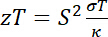
In TE material's, the performance and stability of the properties are essential. Thus, it is important to understand the mechanisms by which the microstructure can be altered and their impact on the properties. In this work, Zn4Sb3 TE material was used to show the feasibility of this method. TE materials utilize a temperature gradient between a hot side and a cold side to directly convert heat into electrical energy32,33. The efficiency of this energy conversion is governed by the dimensionless figure of merit (zT),
 (1)
(1)
where S is the Seebeck coefficient, the electrical conductivity, T the temperature, and k the thermal conductivity.
Among these parameters, the transport properties and can be effectively tuned through microstructural engineering of TE materials, including dislocations4, stacking faults34, grain boundaries35,36,37,38, and precipitates39,40. Electron microscopy is widely used to characterize the microstructure of TE materials. At the microscale, techniques based on scanning electron microscopy (SEM)41,42 are commonly utilized to analyze the grain structure and large secondary phases in the materials43. For resolving nanoscale phases and investigating the atomic structure of defects and interfaces, characterization by TEM and STEM is required39,44,45,46.
TE materials are typically operated from ambient temperature up to several hundred degrees Celsius, and therefore, their transport properties are evaluated over the temperature range in which the material is intended to operate. Additionally, TE materials are subjected to thermal cycling, which may lead to property degradation, including a lower electrical conductivity47. Thermal shocks at the hot side of the device were also reported to cause an increase in electrical resistivity by long-term operation experiments over repeated heat cycles48.
In this work, an optimized FIB-based sample preparation protocol for in situ (S)TEM, in plan-view geometry on MEMS chips for electrical measurements, is presented. By performing all the thinning on the MEMS chip, this method avoids the risk of mechanical failure or artifacts from ion beam-induced damage. Moreover, a protocol to perform electrical measurements under operando heating conditions is also presented to study the temperature-dependent transport behavior. To derive the intrinsic electrical resistivity of the sample in a two-probe setup, electrical measurements were conducted at three stages of FIB thinning, where the sample dimensions (primarily the thickness) were varied. This method provides a framework for correlating structural, compositional, and electrical properties at the nanoscale by in situ and operando measurements.
Protocol
Loading...
$$\rightleftharpoonup{xx}$$
$$\longleftharp{xx}$$,
$$\longrightharp{xx}$$,
1. Extraction and transfer of the TEM sample to the MEMS chip
- In the first step, load the MEMS chip together with the bulk sample, from which the TEM sample will be extracted, into the FIB. Use tweezers with rounded non-conductive tips (e.g., carbon) when handling the MEMS chip to prevent charging. In addition, another straight tweezer with carbon (non-conductive) tips could be helpful for the following steps (Figure 1A,B).
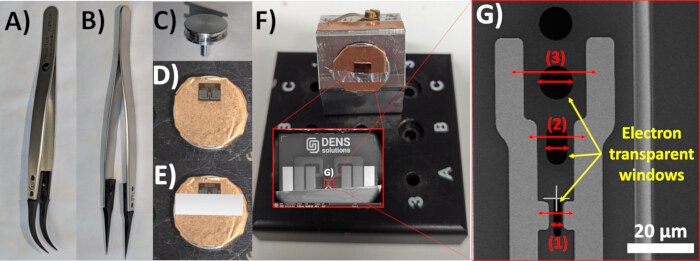
Figure 1: Tools and MEMS chip overview. (A) and (B) Tweezers with carbon/non-conductive tips, (C) standard SEM stub, (D) SEM stub with the Cu-tape and a MEMS chip, and (E) additional Aluminum foil. Also shown are (F) the front side of the pretilt FIB holder with the SEM stub and (G) electron windows on the MEMS chip. The dimensions of the electron transparent windows in (G) are 2 µm (1), 6 µm (2), and 10 µm (3). The TEM sample sizes need to be 10 µm (1), 18 µm (2), and 26 µm (3). Please click here to view a larger version of this figure.
- Use a standard SEM stub (Figure 1C) on which the MEMS chip will be placed.
- Attach some double-sided adhesive Cu-tape on the flat surface of the SEM stub.
- Now, take the MEMS chip out of the chip box using the tweezers with the rounded tip and place it onto the T-pin with the Cu-tape on it. Align the chip so that the writing of the company logo is on the top part of the T-pin (Figure 1D).
CAUTION: The next step should be done carefully. - Cut a small piece of Aluminum foil that can be folded in the middle for better contact onto the MEMS chip. The size should be enough to cover the MEMS chip and part of the Cu-tape, as the Al-foil is going to be stuck on it at each side and below the chip (Figure 1E).
- Position the Al‑foil carefully over the MEMS chip and as close as possible to the suspended SiN membrane. Do not cover this suspended membrane (Figure 1F), as this can lead to the breakage of the membrane of the chip. The TEM sample will be attached to the chip above one of the pre-fabricated holes in the membrane between the biasing electrodes (Figure 1G).
- Vent the FIB microscope for sample insertion.
- Similar to the MEMS chip, put the bulk sample onto another SEM stub or other sample holder. Then position the surfaces of the bulk sample and the MEMS chip horizontally to the stage (plan-view geometry).
- Now insert the stage back in, close the door, and pump the chamber to reestablish the vacuum.
- Start the FIB operation. For this, initialize the electron and ion source.
- First, check the MEMS chip with the secondary electron (SE) image to make sure that the chip has not been damaged. Especially the contacts on the chip and the SiN membrane, as it is very thin (1 µm), should be verified.
- After this, move the stage to image the bulk sample and define the area or region of interest (ROI).
- Adjust the sample to eucentric height, so that the ROI stays in the center for both the electron and ion beam images.
- Next, tilt the stage to 52° (corresponding to 0° with respect to the angle of the ion beam).
NOTE: When the ion beam is used for imaging, the current should always be set to a value smaller than 30 pA, depending on the material (for beam-sensitive samples, even 10 pA or below), to protect the surface, and a voltage of 30 kV is used. For each time a milling pattern is done, the ion beam is paused, and only snapshots with very short times are used to adjust the position or focus at these higher currents before starting the pattern for either milling or deposition. If the sample surface needs to be protected from the ion beam, a thin protection layer of C- or Pt-deposition can now be used, but is not required for this method. The milling can be performed at this point, which means that the TEM sample is cut out of the bulk sample and transferred to the MEMS chip. The dimensions were typically 5 µm x 12 µm (Figure 2A). A larger area than the ROI should be considered, since a small fraction of the sides of the sample might get milled away due to the used currents for rough milling.
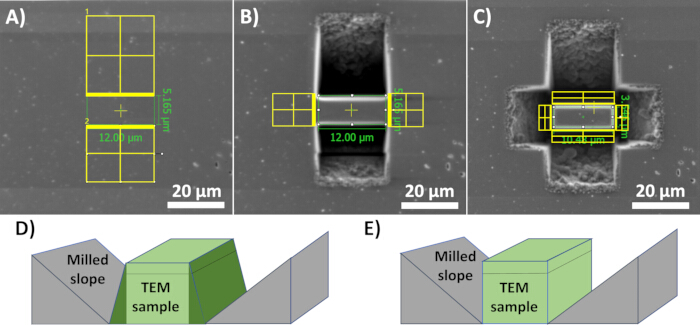
Figure 2: Bulk lamella milling. Dimensions of the plan-view TEM sample in the SEM image. (A) The patterns for the "top" and "bottom" rough milling, and (B) the “right” and “left“ side milling patterns. (D) The tilted sides after (C) the rough milling are flattened out by another milling on all four sides, and (E) are afterward flat. Please click here to view a larger version of this figure.
- First, mill away the “top” part using dimensions of about 13 µm in the x-direction and 14 µm in the y-direction with a depth (z-value) of 10 µm (Figure 2A). Use a “Regular cross section” pattern and a current of 5–15 nA.
- Follow-up by the “bottom” milling (Figure 2A). Again, use a “Regular Cross Section” pattern and a current between 5–15 nA. The dimensions for this milling step are 13 µm in the x-direction and 10 µm in the y-direction. The depth is 10 µm. At this step of the process, the walls of the sample will be slightly tilted (Figure 2D).
- Afterward, mill the sides by milling the “left” and “right” side with the dimensions 6 µm in x-direction and 10 µm in y-direction (Figure 2B). Apply a current of 5–15 nA using the “Regular Cross Section” pattern with a depth of 10 µm.
- After this, perform a rough milling with a reduced current of 1 nA and straightening of all four TEM sample walls (Figure 2E). For this, use a “Cleaning Cross Section” pattern for all four sides (Figure 2C). Apply a current of 1 nA with a z value of 10 µm.
- Tilt the stage to 0° or -5° with respect to the electron beam. An angle of -5° is preferred, since it gives better access for the final milling and follow-up extraction of the sample with the needle as described in the following steps.
- Now extract the TEM sample with a sharp micromanipulator needle. For this, insert the micromanipulator. The used FIB microscope has two options for insertion of the needle, namely, “Insert” and ”Park Position”. Choose the second option since the crashing of the needle into the sample will be prevented that way after the eucentric height is adjusted.
- Carefully lower the needle to the TEM sample.
- Move the needle to the left top corner/edge of the TEM sample.
- Heat up the gas injection system (GIS). Insert the Pt-deposition gas injection system (GIS); the image might move slightly during this procedure, and you may need to adjust the position.
- Choose a “rectangle” pattern to cover part of the needle and the corner of the TEM sample (Figure 3A). The pattern needs to be changed to “deposition” instead of “Si-milling”. Use a current of 30–50 pA with a z height for the deposition pattern of 1 µm.
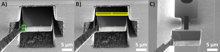
Figure 3: Sample extraction. The pattern for the Pt-deposition (A) after Pt GIS was inserted, and (B) the milling pattern to cut the sample free from the bulk. (C) The sample shadow is visible when close to the MEMS chip surface. Please click here to view a larger version of this figure.
- A “Rectangle” milling pattern and a current of 3 nA are used for cutting (Figure 3B). Choose x-dimension slightly bigger than the length of the TEM sample. Choose a z value of 5–10 µm, depending on the width of your sample. Start the deposition of Pt.
- Afterward, retract the Pt GIS.
- After the TEM sample is cut free, extract the sample with the micromanipulator, only moving it upwards (z-direction) away from the bulk sample. Then retract the needle when the extracted sample is far away from the bulk.
- Move the stage to the MEMS chip. Choose the window for the TEM sample and adjust the eucentric height again. This is done at 0° tilt (Figure 4A).
NOTE: If it is required at this point, the window could now be widened to have a larger window of observation in the TEM. Use a current of 1 nA for this optional step.
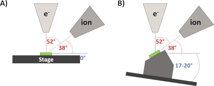
Figure 4: Stage tilts. Schematics of the stage angles (A) for the contacting between the MEMS chip and TEM sample with a stage angle of 0°, and (B) the angle of 17–20° for the thinning part with the 52° pretilt holder. Please click here to view a larger version of this figure.
- Insert the micromanipulator with “Park Position”.
- Carefully lower the micromanipulator with the TEM sample to the surface of the MEMS chip. Center the TEM sample above the window (black area).
CAUTION: Cautiously lower the TEM sample down to the chip. A shadow of the sample can be seen appearing over the MEMS chip shortly before the touchdown (Figure 3C). Stop before touching the chip with the sample. - Insert the Pt GIS system again.
- Further lower the sample until it touches the chip. Usually, a slight change in contrast in the image can be observed when contact has been established.
- Start a pattern for Pt deposition and weld the TEM sample by making two similarly sized patterns (Figure 5A). For this, utilize a “Rectangle” pattern with a current of 30–50 pA. Do the first gluing with a pattern of 4 µm in x, 1 µm in y, and 1 µm in z.
NOTE: Note down the rotation angle in the first step, then do +90° with each step for the welding. - After this, cut the needle from the TEM sample with a current of 0.3 nA and retract it. Avoid cutting through the biasing electrodes.
- Now rotate the sample by 90°. Do another pattern with dimensions of 2.5 µm in x, 1.5 µm in y, and 1 µm in z (Figure 5B). Use a current of 30–50 pA with a “Rectangle” pattern.
- Now do the third gluing with a rotation angle of 180° (+90°) relative to the noted 0°. Choose the same dimensions as in step 1 for gluing. The current is set again to 30–50 pA and uses a “Rectangle” pattern (Figure 5C).
- Again, rotate to the fourth side with a 270° rotation angle (another +90°). Use the same dimensions as in step 1.33 with a current of 30–50 pA and a “Rectangle” pattern (Figure 5D).
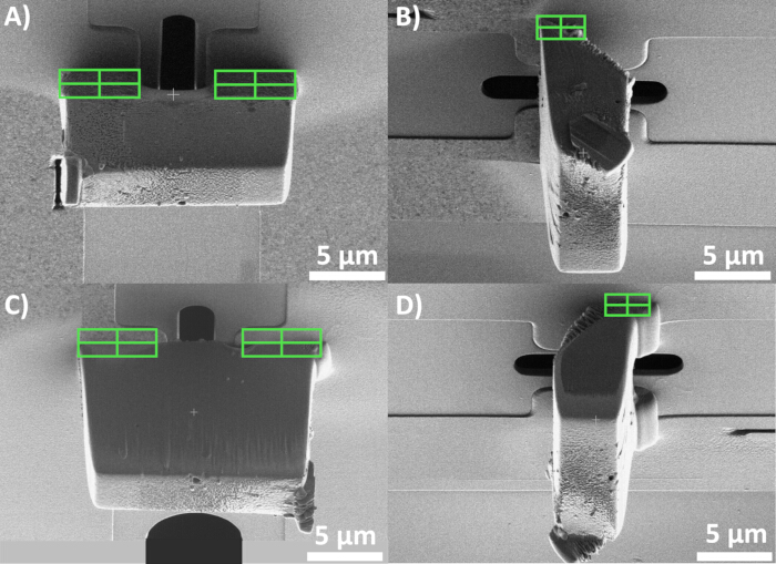
Figure 5: Welding of the sample to the MEMS chip. Welding of the TEM sample to the MEMS chip (A) from the front side, (B) rotated by 90°, (C) rotated an additional 90° to a total of 180°, and (D) final rotation to a total degree of 270°. Please click here to view a larger version of this figure.
- Extract the Pt GIS after the gluing is done and vent the vacuum chamber.
- Now, take the sample out of the FIB and put the SEM stub with the MEMS chip on top on a pretilt holder with an angle of 52° (Figure 1F). The pretilt holder is necessary for the following thinning steps.
NOTE: This step is done because of spatial limitations by tilting and moving the stage when both the tilted holder and the bulk sample are directly inserted to protect both the pole-pieces of the electron and ion column from touch alarm with the chip, tilted holder, or bulk sample. This achieves easier operation inside the device. Here, a pause is possible, as the next steps can be performed later or in another FIB session.
2. Thinning of the TEM sample on the MEMS chip
NOTE: For the thinning, the used currents were chosen according to the mechanical properties of the Zn4Sb3 material. The currents should, in general, be chosen according to the hardness of the material to be milled (hard material = higher currents, softer materials = lower currents).
- Insert the SEM stub with the MEMS chip on the pretilt FIB stub, which has a 52° angle. Close the FIB door and pump the chamber.
- The thinning is done now as the last part. For this, tilt the stage to 17–20° (Figure 4B). The vertical angle between the thinning direction and the ion beam would be at 14°, but an over-tilt allows for thinning on both the bottom and top sides of the TEM sample. Additionally, the over-tilt prevents charging during thinning.
NOTE: From now on, the sample is observed in side view (Figure 6) in the FIB image. - Now mill a large part of the TEM sample above the electron transparent window (Figure 6A) with a voltage of 30 kV and a current of 0.05–1 nA until a thickness of about 2 µm is reached (Figure 6B). Choose a z value for this cut that is a bit higher than the TEM sample width to ensure that the sample is cut through (Figure 6B).
- Now, perform iterative thinning steps with a “Cleaning Cross Section” pattern. First, use a current of 0.1 pA in this first step and tilt the stage by ± 1.5° for thinning of both sides (“‑“ accounts for thinning of the “bottom” part in the image and “+” for the “top” part) with respect to the ion beam direction (Figure 6C). Use a z value of 2 µm. Do this each time for about 20–30 s from each side.
NOTE: Measure the thickness after a couple of these iterations. - When reaching a thickness of less than 1 µm, lower the current to 30–50 pA. After this, vary the tilt angle by ± 1° with respect to the ion beam. Again, use the “cleaning cross section” pattern for this with a z value of 2 µm (Figure 6D).
- When reaching a thickness of about 500 nm, lower the current to 10–30 pA. Again, use a pattern with “cleaning cross section” and tilting by ± 1° (Figure 6E). Use a z of 2 µm and mill iteratively on each side until a thickness of about 200 nm is reached.
- For further thinning below 500 nm, lower the voltage to 5 kV and set the current to 48 pA. Use the “Cleaning Cross Section” pattern for this step as well. Now tilt by ± 2° and lower the z to 0.1 µm. Do this again iteratively until the desired thickness is reached.
- Measure the thickness every couple of iterations in the SE image again, as this is more accurate than in the ion beam image.
- As a last step, when the desired thickness is reached, clean the surface of the lamella with a voltage set to 2 kV and a current of 27 pA. Again, use a “Cleaning Cross Section” pattern and a tilt of ± 5° with a low z of 0.03 µm. Do the cleaning from each side for a few seconds.
- Measure the final dimension of the thickness, length, and width of the thinned region (lamella). The thickness and length are measured from the side view (Figure 6F) and the width from a top view.
NOTE: The dimensions can be changed in different milling steps. Different dimension steps are then used to evaluate the material's electrical resistivity, shown in the Representative Results section.
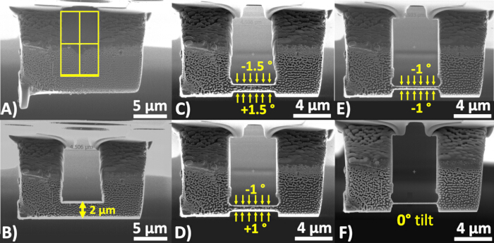
Figure 6: Lamella thinning. View of the FIB image on the TEM sample for (A) the “rough” thinning and (B) the leftover part after the rough milling with a thickness of about 2 µm. Thinning steps up to a thickness of (C) 1 µm, (D) 500 nm, (E) below 500 nm until 200 nm, and (F) final thickness that is measured. The arrows indicate the tilting and thinning from each side in iterative steps. Please click here to view a larger version of this figure.
3. In situ heating and biasing experiments inside the (S)TEM
- Insert the MEMS chip into the sample holder.
- After this, insert the holder into the (S)TEM device and connect it to the in situ setup.
- The setup includes a heating control unit for the temperature and a source meter to control the electrical biasing. The interconnect unit combines both devices to control the MEMS chip. Connect the heating unit and the source meter to a laptop with USB-C cables. Connect the in situ setup as shown in Figure 7.
- The source meter has an output of Force-LO (F-LO) and Force-HI (F-HI). Connect these to the interconnect unit input 1 and 6, respectively (black cables in Figure 7).
- Next, connect the heating control unit with the interconnect unit (red cable in Figure 7).
- Ground the interconnect unit, the heating control unit, and the source meter (yellow cables, Figure 7).
- Start the Source meter.
NOTE: Make sure that whenever the source meter is turned on or off, disconnect the cable from the interconnect unit to the sample holder to prevent discharge. - After finishing the setup, connect the cable going out from the interconnect unit to the holder in the (S)TEM (blue cable in Figure 7). It is best to already observe the sample when connecting the cable to check if some discharge takes place, which could destroy the sample. To prevent this, always turn on the source meter before connecting the cable from the interconnect unit to the sample holder.
NOTE: The holder itself is disconnected from the ground, or otherwise it would trigger a pole-touch error. - Start the computer. Use the instrument-specific control software on the laptop. Start the software and choose the input conditions (e.g., temperature, voltage, current).
- Now, calibrate the temperature. The temperature coefficient of resistance (tcr) number is printed on the packaging of the box with the MEMS chips. Insert this value in the software. Calibrate the temperature after inserting the number.
- Start the experiment, and two graphs of temperature and current/voltage over measurement time are shown.
- Set the temperature. For each temperature step, the voltage is swept within the chosen range automatically when choosing ramp biasing in the software. Alternatively, choose a constant biasing voltage.
- For an experiment to start, set the range for voltage sweeping (e.g., 1 mV) or choose a constant voltage.
- After the measurement, stop the experiment and save the data.
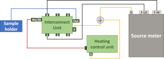
Figure 7: Biasing and heating setup. Schematic of the setup for in situ biasing and heating experiments, including the source meter, heating control unit, and an interconnect unit to combine the heating and biasing inputs with an output (“Out”) to the sample holder. The yellow color denotes the grounding connection of the devices, the red color the connection of the heating and interconnect unit, the blue is the connection to the sample holder, and the black connections are for the electrical measurements. The 4H/2B port refers to the in situ chip setup with 4 heating and 2 biasing contacts. Please click here to view a larger version of this figure.
Results
Loading...
$$\rightleftharpoonup{xx}$$
$$\longleftharp{xx}$$,
$$\longrightharp{xx}$$,
Following the protocol, samples are prepared from bulk polycrystalline thermoelectric Zn4Sb3 for the operando (S)TEM experiments. The total resistance (R) is measured with a source meter, as detailed above.
As shown in Figure 8, the voltage (V) is swept between ±1 mV (Figure 8A), and the resulting current (I) is recorded in Figure 8B. The current has a linear relationship with the applied voltage, showing the Ohmic behavior (Figure 8C). The electrical resistance R can thus be calculated from the slope of the I ‑ V curve using Ohm’s law:
 (2)
(2)
The slope of the I-V curve is determined as R = 257 Ω (Figure 8).
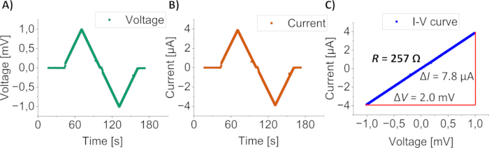
Figure 8: I-V curve. (A) The sweeping of the voltage, (B) the resulting current, and (C) the I-V curve at room temperature, with the resistance measured as the slope of the I-V curve. Please click here to view a larger version of this figure.
To measure electrical resistance as a function of temperature, MEMS-based heating was applied to the chip. The sample was heated in steps from room temperature (21 °C) to 50 °C, 100 °C, 150 °C, and 200 °C (for the second ramp up also to 250 °C and 300 °C) and cooled back in the same temperature steps (Figure 9A).
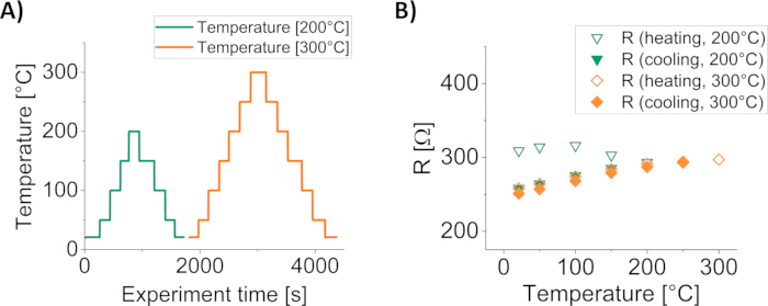
Figure 9: In situ heating and cooling in TEM. (A) The temperature applied during heating-cooling cycles up to 200 °C and 300 °C plotted over experiment time, and (B) the corresponding total resistance (R) measured at each temperature step, with R measured during heating represented by open symbols and cooling by closed symbols. Please click here to view a larger version of this figure.
As shown in Figure 9B, R values measured from the first heating cycle from 21 °C to 200 °C are higher than the R values measured in the cooling steps from 200 °C to 21 °C. Afterward, the sample was heated a second time from 21 °C to 300 °C (Figure 9A). For this second heating cycle, R is not changed when heating up or cooling down compared to the first cooling curve (Figure 9B), and hence the resistance measurement is reproducible.
To evaluate the intrinsic electrical resistivity of the sample, a resistance circuit is drawn for the setup, which includes the various contributions to the measured resistance R (Figure 10).
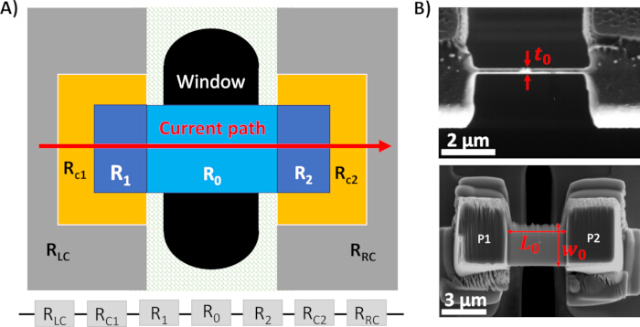
Figure 10: Resistance circuit of the sample and contacts. (A) The schematics of the setup, including all the contributions to the total resistance (R) with the resistance circuit and (B) the dimensions for the lamella in length (L0), width (w0), and thickness (t0), together with the two pillars (P1 and P2). Please click here to view a larger version of this figure.
When a current is applied through the sample, there will be a resistance due to the electrodes on the MEMS chip (RLC and RRC), the resistance of the Pt-C deposition material, which was used for the welding of the sample onto the chip (RC1 and RC2). The sample consists of three shapes: the lamella (R0) and the two pillars (R1 and R2). The total resistance can then be expressed as:
 (3)
(3)
with the dimensions of length (L0), width (w0), and thickness (t0) that were measured in the FIB, the intrinsic electrical resistivity (ρ), as well as the combined resistance Rc = RLC + RRC +RC1 + RC2 + R1 + R2.
If Rc is known, the electrical resistivity (ρ) can be calculated from the operando measurements of R by rearranging equation 3:
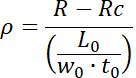 (4)
(4)
As Rc is not negligible and usually not known, another method is required to derive the ρ values for each temperature.
According to equation 4, the total resistance R changes with the sample dimensions (L, w, t). As shown in Figure 10B, during three different stages of lamella thinning in the FIB (step 2.9), the sample had different dimensions, primarily differing in their thickness, as shown in Table 1.
| Dimensions for 1.8 µm thickness: | Dimensions for 0.5 µm thickness: | Dimensions for 0.2 µm thickness: | |||||||||||
| w1 | L1 | t1 | w1 | L1 | t1 | w1 | L1 | t1 | |||||
| 4.25 | 5.70 | 3.81 | [µm] | 4.2 | 6.20 | 3.81 | [µm] | 4.2 | 6.35 | 3.81 | [µm] | ||
| w0 | L0 | t0 | w0 | L0 | t0 | w0 | L0 | t0 | |||||
| 3.65 | 4.27 | 1.77 | [µm] | 2.70 | 4.35 | 0.48 | [µm] | 1.70 | 4.35 | 0.22 | [µm] | ||
| w2 | L2 | t2 | w2 | L2 | t2 | w2 | L2 | t2 | |||||
| 4.10 | 5.75 | 3.33 | [µm] | 4.20 | 6.10 | 3.33 | [µm] | 4.20 | 6.25 | 3.33 | [µm] | ||
Table 1: Sample dimensions. Dimensions of the three sample geometries measured during the different stages of lamella thinning.
As the R measurements were repeated at the three different dimensions, the reproducible R values from the cooling steps from 200 °C to 21 °C were taken and plotted as a function of the dimensions  according to
 (5)
(5)
where R(T), ρ(T) and only represent the different temperatures at which the sample was measured during stepwise heating and cooling for each thickness. The plot is linear according to equation 5, where the slope of R corresponds to ρ(T), while the intercept at the vertical axis is the (Figure 11).
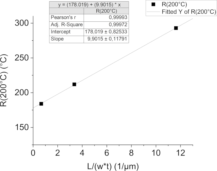
Figure 11: Linear fitting of resistance to sample dimensions. Example plot for the measured R at 200 °C in three milling steps with different lamella dimensions (Table 1). The slope of the fitted curve corresponds to ρ. Please click here to view a larger version of this figure.
The same plot and linear fitting are performed for each temperature during the cooling steps, where the measured R is reproducible. The slopes and intercepts of the fitted datapoints return ρ and the combined resistance Rc (equation 3), respectively. As plotted in Figure 12, both ρ and Rc can be determined as a function of temperature.
![Temperature-dependent resistivity and Rc(Ohm) chart; ρ(T), Rc plotted vs. temperature [°C].](/files/ftp_upload/68886/68886fig12.jpg "figure-results-10")
Figure 12: Sample electrical resistivity. Plots of the electrical resistivity ρ and combined resistance Rc as defined in equation 4. Please click here to view a larger version of this figure.
As the temperature increases, ρ also increases from 8.8 µΩ∙m at 21 °C to 9.9 µΩ∙m at 200 °C. This is expected for a degenerate semiconductor and fits the measurements on Zn4Sb349. Rc is observed to increase from about 150 Ω at 21 °C to 178 Ω at 200 °C, which is also expected for metals and degenerate semiconductors.
During the electrical measurements, the microstructure of the sample after the final thinning step (0.2 µm thickness) was observed using a TEM device operated in the STEM mode (Figure 13A). The microstructure was stable during the temperature range (21 °C to 300 °C) of the resistivity measurements. The average grain size of the Zn4Sb3 sample remains 300 nm after the heating-cooling cycles up to 300 °C (Figure 9A).
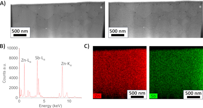
Figure 13: Microstructure and composition. (A) Annular bright field-STEM micrographs of the Zn4Sb3 sample before and after the heating-cooling cycles up to 300 °C, (B) integrated EDS spectrum of the lamella, and (C) elemental maps showing the homogeneous distribution of Zn and Sb. Please click here to view a larger version of this figure.
As shown in Figure 13B, the total energy dispersive X-ray spectroscopy (EDS) spectrum shows clear peaks of Zn and Sb. The elemental maps in Figure 13C show a homogeneous distribution of Zn and Sb. Elemental quantification yields 56.6 at.% Zn and 43.4 at.% Sb, fitting to the nominal composition of Zn4Sb3 (57.1 at.% Zn, 42.9 at.% Sb). Using this operando procedure, it is feasible to track the microstructural evolution of the sample under heating and electrical biasing, and it correlates to the measurements on materials properties ρ.
Discussion
Loading...
$$\rightleftharpoonup{xx}$$
$$\longleftharp{xx}$$,
$$\longrightharp{xx}$$,
Reduction in contact resistance during heating
The slopes of the heating and cooling curves show a variation in the measurements of R. The measurements of R for the different dimensions (primarily thickness) of the cooling curve showed all points closely fitting on one line according to equation 5 (Figure 14A). In contrast, the heating curve showed large variation between the different R values at the same temperature and thus the slope (Figure 14B). These different slopes (indicated by the blue and red lines in Figure 14B) would result in different values for ρ as well as Rc and would yield inconsistent measurements.
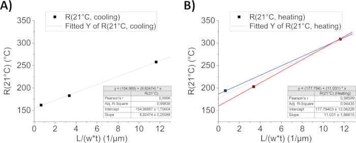
Figure 14: Uncertainty in electrical resistivity. The plotted R for the three different dimensions of the sample, showing R from (A) the cooling (200 °C to 21 °C) at 21 °C, and (B) the heating (21 °C to 200 °C), measured R at 21 °C, with the blue and red lines indicating the deviations. Please click here to view a larger version of this figure.
As shown in Figure 14B, the uncertainty for the linear fit of the heating curve is 7.4% for Rc and 17.3% in ρ. Whereas for the cooling curve (Figure 14A), the uncertainty is only 1.2% for Rc and 2.8% in ρ. Thus, for reliable measurements of ρ and Rc, only R values from the cooling curve should be used.
The difference between the R measurements between the heating and cooling curves can be attributed to the following reason. In a previous study on Pt-C contacts for in situ heating and biasing, Zhong et al.50 showed that the total resistance can be lowered by annealing above 100 °C, due to the reduction in resistance of the Pt-C composite. As schematically shown in Figure 15, the Pt-C contacts were deposited as Pt nanoparticles in an amorphous C matrix. During annealing, the contact turned to Pt networks with higher connectivity between Pt nanoparticles and hence reduced resistance. From the performed experiments, heating to 200 °C was sufficient to reach reproducible R values. No further resistance decrease was observed with heating up to 300 °C.
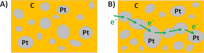
Figure 15: Possible mechanism of reducing contact resistance. Schematics of (A) the Platinum (Pt) nanoparticles that formed (B) partial conductive pathways surrounded by Carbon (C). Please click here to view a larger version of this figure.
Current leakage in electrical measurements
As shown in Figure 16, leakage paths can form between the electrodes due to the Pt deposition steps (step 1.31–1.36) during FIB preparation. In Figure 16A, the green shades indicate the approximate areas where residues from Pt-C welding can be observed (steps 1.31–1.36).
To account for such leakage paths due to residues from Pt-C deposition, a leakage resistance Rleak needs to be introduced in parallel to the sample (R1, R0, and R2) and welding (RC1 and RC2) resistance (Figure 16B). The resistance circuit for such a parallel leakage path is shown in Figure 16C.
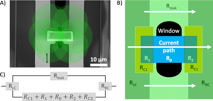
Figure 16: Leakage path resistance circuit. (A) Secondary electron image taken in FIB during preparation shows deposition of Pt-C after the first welding step (1.31), (B) the schematics of the leakage current and current through the sample, and (C) the resistance circuit for this setup. The transparent green color in (A) and (B) indicates the residue Pt-C layer from the welding (steps 1.31–1.36). Please click here to view a larger version of this figure.
To evaluate Rleak, a lamella was totally cut off to block the electrical path through the sample, leaving only the leakage path (Figure 16B). In this case, Rleak was determined as 4 kΩ. Note that this value would vary depending on the Pt-C welding procedure, and only serves as an order of magnitude estimate. In this case, the measured R values (200–300 Ω, Figure 9) are much smaller than Rleak, so that the effect of the leakage path remains small. However, for materials with higher resistivity, the resulting R values can exceed 1 kΩ, leading to a significant effect from the leakage path, or even a dominant effect from the leakage path for measured R values exceeding 10 kΩ. In order to reliably measure samples with higher resistance, additional steps are required to maximize Rleak. As noted in step 1.26 of the protocol, the vacuum window on the chip can be extended by FIB milling. This should be done with a 20–30 µm cut above and below the window above which the sample is positioned, as the residue was observed mainly within a radius of 10 µm. This increased window effectively blocks the leakage path through the Pt-C residue between the two electrodes, leading to Rleak > 100 MΩ. By extending the vacuum window, materials with much higher electrical resistance can be reliably measured.
It is also noteworthy that residues from Pt-C deposition are also present on the surface of the sample pillars, as shown in Figure 6A. The effect of such leakage paths is only shown in the combined resistance Rc term in equation 3, as the lamella has been thinned down to be free of Pt-C deposition.
In summary, a protocol for the sample preparation on in situ biasing and heating MEMS chips via FIB is shown. The method uses a one-step transfer of a plan-view sample to the MEMS chip, followed by direct thinning on the chip. This enables simple preparation of TEM samples and minimizes mechanical or ion beam damage. The electrical resistivity can be determined as a function of temperature. This enables operando microstructural characterizations with direct correlation to the electrical properties of the sample. Despite using 2-point probe electrical measurements, contributions from the intrinsic sample resistance and contact resistances can be separated by resistance measurements after different stages of FIB milling with various sample dimensions. Using this approach, intrinsic electrical properties of TEs and many materials in electrical and energy applications can be evaluated during operando microscopic characterizations.
Disclosures
Loading...
$$\rightleftharpoonup{xx}$$
$$\longleftharp{xx}$$,
$$\longrightharp{xx}$$,
The authors have nothing to disclose.
Acknowledgements
Loading...
$$\rightleftharpoonup{xx}$$
$$\longleftharp{xx}$$,
$$\longrightharp{xx}$$,
We acknowledge Dr. Vesna Srot for constructive feedback on the manuscript. D.A.M. acknowledges funding from the International Max Planck Research School for Sustainable Metallurgy (IMPRS SusMet). C.J. acknowledges the Global Joint Research Program funded by Pukyong National University (202506170001). C.S. and S.Z. acknowledge the German Research Foundation (DFG) for funding within the Collaborative Research Center SFB 1394 “Structural and Chemical Atomic Complexity—From Defect Phase Diagrams to Materials Properties” (Project ID 409476157, project group B01).
Materials
| Name | Company | Catalog Number | Comments |
|---|---|---|---|
| Gas Injection System (FIB) | Thermo Fisher Scientific | 1346158 | Catalog number used to order directly from Thermo Fisher Scientific |
| Heating control unit | DENSsolutions | 180200304 | with cables |
| Inter connect unit | DENSsolutions | 160800114 | with cables |
| Lightning system holder | DENSsolutions | - | |
| MEMS chips | DENSsolutions | 4 heating and 2 biasing contacts, also possible for 4 biasing and 2 heating contacts | |
| Software: Impulse | DENSsolutions | Version 1.2.0.0 | software on laptop provided by DENSsolutions |
Reprints and Permissions
Request permission to reuse the text or figures of this JoVE article
Request Permission