This work presents a simulation-based dynamic wireless power transfer (DWPT) system using a double-D (DD) coil structure in a dual-transmitter single-receiver (DTSR) topology and dual-loop proportional–integral (PI) control strategy, demonstrating regulated voltage and power delivery under coupling variation, misalignment effects, and a 150 mm air gap.
A subscription to JoVE is required to view this content. Sign in or start your free trial.
Research Article
Dual-Loop PI Control for a Dynamic Wireless Electric Vehicle Charging System with Dual-transmitters using 3D Modeling of DD Coils
In This Article
Summary
Abstract
Dynamic wireless power transfer (DWPT) is an emerging technology for supplying electric vehicles (EVs) with energy while in motion; however, its performance is significantly affected by coupling variation, coil misalignment, and load fluctuations. To address these challenges, this study presents a simulation-based protocol that integrates electromagnetic modeling, circuit-level co-simulation, and coordinated control evaluation for a dual-transmitter single-receiver (DTSR) DWPT system. The methodology begins with three-dimensional electromagnetic modeling of a double-D (DD) coil configuration using a finite-element solver to characterize self- and mutual-inductance variations under misalignment conditions. These parameters are then incorporated into a resonant circuit model to optimize power transfer performance. The complete DTSR system is subsequently implemented in a system-level simulation environment, where a dual-loop proportional–integral (PI) control strategy is applied to regulate output voltage and power under time-varying coupling conditions. The results demonstrate stable power delivery and effective regulation performance across dynamic operating scenarios, including a fixed air gap of 150 mm and varying misalignment conditions. The proposed framework enables systematic evaluation of system dynamics, control response, and power stability. This protocol provides a structured and reproducible workflow for analyzing and validating DTSR-based DWPT systems and supports the development of robust control strategies for dynamic EV charging applications.
Introduction
Electric vehicles (EVs) have emerged as a competitive alternative for transportation due to their advantages in environmental friendliness, isolation, and safety1,2. However, EVs face several constraints, most notably limited battery autonomy, which results in restricted driving range, high cost, and lengthy charging times3,4. Wireless power transfer (WPT) technology is considered a key enabler for overcoming these limitations by providing convenient and continuous energy supply. This charging technology can be categorized into two groups: static charging, where the vehicle is stationary over the charger, and dynamic wireless power transfer (DWPT), which enables power transmission while EVs are in motion5–8. DWPT has emerged as a promising approach for reducing battery dependency, improving mobility, and saving time9.
In EV-DWPT technology, the primary research areas include coil design and system topology. Various coil structures have been proposed, among which the double-D (DD) coil is widely adopted for EV-DWPT applications10. Coil sizing and optimization with respect to coupling coefficient, cost, and efficiency have been extensively studied11,12. In addition, modular EV-DWPT topologies with different configurations have been investigated to maintain high efficiency13–16. The efficiency of EV-DWPT systems is strongly influenced by the design of transmitter and receiver pads10,17,18, as coil geometry affects coupling coefficient, self-inductance, misalignment tolerance, electromagnetic field (EMF) exposure, and power transmission characteristics19. Design parameters include coil geometry, shielding, materials, axial and lateral misalignment, and dimensions. Although several pad geometries exist (circular, rectangular, DD, DDQ, etc.), DD pads are widely used due to their high mutual inductance (M) and industry adoption, as recommended by the Society of Automotive Engineers (SAE J2954)20. Recent studies have investigated the calculation of self- and mutual inductance under misalignment conditions using analytical, numerical, experimental, and simulation approaches21–25.
Most existing research focuses on conventional single-transmitter single-receiver (STSR) EV-DWPT systems, which face limitations in high-power applications and rapid charging capability16,26. To address these limitations, dual-transmitter single-receiver (DTSR) configurations have been proposed to increase power transfer capacity by providing multiple transmission paths. Optimized DTSR designs using DD coils with LCC compensation have been developed to enhance power transfer efficiency27, while theoretical modeling and impedance matching techniques have been investigated to further improve performance under dynamic conditions28. However, misalignment reduction in multi-transmitter systems remains a significant challenge, and various design strategies have been proposed to mitigate this issue29. Additionally, DTSR systems operating at a common resonance frequency with energy-saving techniques have been introduced and experimentally validated30.
Despite these advancements, optimal system performance in EV-DWPT cannot be achieved without effective control strategies. Control methods are generally classified into primary-side, secondary-side, and dual-side control approaches31. For instance, a DC–DC converter with a proportional–integral (PI) controller has been used on the secondary side to regulate output voltage under varying load and coupling conditions32. On the primary side, the phase-shift angle of the full-bridge inverter is commonly controlled to regulate power transfer while maintaining zero-voltage switching (ZVS) at resonance33,34,35. However, existing DTSR DWPT studies typically address electromagnetic design, resonant compensation, or control strategies separately. In contrast, this work integrates these components within a unified system-level framework to evaluate their combined impact under dynamic operating conditions.
The proposed procedure combines three-dimensional finite-element modeling and magnetic optimization of DD coils, circuit-level co-simulation for compensation network design and efficiency assessment, and coordinated control implementation using a dual-loop PI structure. The inner control loop regulates the secondary-side DC–DC buck converter to stabilize the load voltage under variable conditions, while the outer loop adjusts the phase shift of the primary-side full-bridge inverter to achieve adaptive power transfer in response to coupling variations.
The system adopts a series–series (SS) compensation network to minimize reactive power at resonance and improve overall efficiency, with the operating frequency fixed at 85 kHz to ensure consistent parameter evaluation36. Rather than proposing a new control algorithm, this study's contribution lies in the systematic integration of a conventional dual-loop PI controller into a complete electromagnetic–circuit–control co-simulation framework for DTSR DWPT systems, enabling coordinated voltage and current regulation.
The resulting framework demonstrates stable power delivery under representative dynamic charging conditions and extends the applicability of established dual-loop PI control strategies to DTSR EV charging systems. The proposed methodology is particularly suitable for resonant inductive EV charging systems with similar pad geometries and operating conditions, though adaptation may be required for non-resonant architectures or highly nonlinear, time-varying loads. A workflow diagram illustrating the simulation stages is provided in Figure 1.
Access restricted. Please log in or start a trial to view this content.
Protocol
The research tools employed are listed in the Table of Materials.
1. 3D finite-element modeling of DD coils
The electromagnetic modeling and optimization of transmitter and receiver DD coils were implemented using a 3D finite-element electromagnetic solver. The transmitter coil dimensions were optimized by sweeping length and width, while the receiver coil dimensions and the distance between the coils were kept fixed. The magnetic coupling between both sides was measured, and its mathematical representation is given by31:
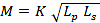 (1)
(1)
where  represents the coupling coefficient describing magnetic coupling between the coils,
  denotes the self-inductance of the transmitter coil, and
  represents the self-inductance of the receiver coil.
Based on the recorded maximum magnetic coupling, the transmitter length and width were selected. The receiver coil was designed with a smaller width than the transmitter to improve misalignment tolerance and mid-range coupling29. The optimized dimensions and specifications were presented in Figure 2 and Table 1.
During modeling, the coils were excited with sinusoidal current sources at 85 kHz, and magnetic resonance coupling was enabled via series compensation capacitors. Adaptive meshing was employed, with refinement concentrated in regions of high magnetic field intensity, particularly around the transmitter and receiver coils. The self-inductance, mutual inductance, and coupling coefficient were directly extracted from the field solutions using built-in parameter-extraction tools.
2. WPT circuit co-simulation
To evaluate the system power transfer efficiency (PTE) at the selected frequency, the extracted electromagnetic parameters were imported into a circuit simulation environment (see Table of Materials), and WPT circuit co-simulation was performed. A time-domain circuit solver was used to simulate the interaction between the power electronic converter and the coupled coil model under dynamic operating conditions. The compensation elements were tuned to satisfy the resonance condition defined by:
 .(2)
.(2)
where  represents the primary compensation component.
The air gap between the coils was fixed at 150 mm. The maximum PTE was estimated at approximately 0.0851 MHz as the operating frequency under the given spacing constraints. The maximum PTE was estimated at approximately 0.0851 MHz at an operating frequency under the given spacing constraints. The results indicated that magnetic resonance-based coupling achieved higher efficiency at mid-range distances compared to alternative wireless power transfer approaches, supporting its suitability for dynamic charging applications.
3. DWPT system implementation
The 3D coil model of the DTSR system implemented in the finite-element electromagnetic solver was presented in Figure 3. The receiver coil motion was defined along the Y-axis (lateral misalignment), while the X-axis displacement was assumed to be zero. The Z-axis represented the air gap between the coils, which was set to 150 mm. The mutual inductance  became a function of displacement, expressed as
  .
.
The receiver coil moved from (0, −80, 150) mm to (0, 1400, 150) mm in the xyz coordinate system, resulting in a total lateral displacement of 2700 mm along the Y-axis. The simulation was performed to evaluate the variation of with lateral misalignment. The numerical results presented in Figure 4 and Supplementary Table 1 indicated peak mutual inductance at positions 9 and 22, corresponding to alignment with transmitter 1 and transmitter 2, respectively.
The circuit diagram of the proposed DWPT system was shown in Figure 5. The system consisted of two grounded transmitters  and
and  , and one moving receiver . The transmitters were supplied by a DC source connected to a full-bridge inverter, which converted DC voltage into high-frequency AC required for magnetic resonance coupling. The output was fed into a compensation network to achieve resonance, improve efficiency, and enhance power transfer37. Common compensation topologies were discussed in previous studies38.
The proposed system adopted a series–series (SS) compensation network, which minimized impedance at resonance and reduced reactive power. Capacitors  and
and  formed the primary compensation network, while
  represented the secondary compensation component.
The DWPT system was simulated at the system level using the parameters given in Table 2. The induced voltage depended on the mutual inductance , which varied with coil displacement during motion. The system behavior under varying lateral displacement was analyzed by observing mutual inductance, voltage, and current in both transmitter and receiver coils. For simulation purposes, a vehicle speed of 27 m s⁻1 (~60 mph) was used.
The mutual inductance, transmitter voltage, and current are shown in Figure 6, where a zero-phase shift indicates operation at resonance. The receiver voltage and current were presented in Figure 7. The load voltage and current are shown in Figure 8, and the output power is shown in Figure 9. Variations in load characteristics were observed due to changes in mutual inductance and coupling coefficient, which were addressed through the control strategy described in the next section.
4. Control methodology
A dual-side control approach was employed due to its effectiveness in enhancing power transfer and system efficiency under varying coupling conditions39,40. A dual-loop proportional–integral (PI) control strategy was adopted to regulate both voltage and current.
The controller parameters were selected based on cascade control design principles rather than empirical tuning. The inner current loop, associated with the secondary-side DC–DC buck converter, was designed with a higher bandwidth to ensure fast response and disturbance rejection. The outer loop, controlling the primary-side phase-shift full-bridge (PSFB) inverter, operated at a lower bandwidth to maintain loop decoupling.
The PSFB control strategy involved continuous measurement of output voltage or current at the receiver, which was fed back to the inverter. The output power was controlled by adjusting the phase shift between the inverter legs, with a larger phase shift resulting in increased power transfer. The PI controller determined the required phase shift and generated pulse-width modulation (PWM) signals for switching control. The overall control structure was illustrated in Figure 10.
The control system was implemented in a discrete-time simulation environment with a fixed sampling period sufficient to capture the 85 kHz switching dynamics. Controller gains were tuned to achieve stable operation with minimal overshoot and acceptable settling time under variations in load and coupling conditions, while maintaining adequate stability margins.
Validation of the control design was achieved when the cascaded PI structure produced rapid, smooth voltage recovery under disturbances and when the inner current loop responded faster than the outer voltage loop. Deviations from these characteristics indicated potential inconsistencies in parameter extraction, compensation tuning, or controller configuration.
Access restricted. Please log in or start a trial to view this content.
Results
Coil optimization sweep
The dimensions of the primary and secondary DD coils were determined based on the parametric sweeping procedure described in the protocol. The measured magnetic coupling between both sides during primary coil dimension sweeping indicated that the maximum coupling coefficient was achieved at a transmitter length of 500 mm and a width of 370 mm, with values of 0.349204 and 0.337464, respectively, as shown in Figure 11. Based on these results, the op...
Access restricted. Please log in or start a trial to view this content.
Discussion
The main research gap addressed in this work concerned the limited dynamic stability and regulation accuracy of conventional single-loop or uncontrolled DWPT systems, particularly under load variations and coupling fluctuations caused by vehicle motion, as highlighted in previous studies on dynamic wireless charging systems7,8. The results demonstrated that the proposed dual-loop PI control architecture for the DTSR configuration directly addressed this limitatio...
Access restricted. Please log in or start a trial to view this content.
Disclosures
Aveen Uthman Hassan conceived the study, designed the methodology, performed the simulations, analyzed the results, and drafted the manuscript. Fadhil T. Aula contributed to technical supervision, result interpretation, and manuscript revision. All authors reviewed and approved the final manuscript.
Acknowledgements
Access restricted. Please log in or start a trial to view this content.
Materials
| Name | Company | Catalog Number | Comments |
|---|---|---|---|
| ANSYS Electronics Desktop (Maxwell 3D) | Ansys, Inc.Maxwell (version 2018) | N/A | Integrated electromagnetic platform hosting ANSYS Maxwell used for finite-element electromagnetic modeling of DWPT coils |
| ANSYS Electronics Desktop (Simplorer) | Ansys, Inc.Simplorer (version 2018) | N/A | Commercial circuit-level simulator used to implement resonant DWPT model |
| MATLAB/Simulink | MathWorks, Inc.(version R2023b) | N/A | Control design and simulation environment used for controller implementation and dynamic system simulation |
References
- Covic, G. A., Boys, J. T. Modern trends in inductive power transfer for transportation applications. IEEE J Emerg Sel Top Power Electron. , (2013).
- Kashem, M. A., Shamsuddoha, M., Nasir, T. Sustainable transportation solutions for intelligent mobility: a focus on renewable energy and technological advancements for electric vehicles (EVs) and flying cars. Future Transp. , (2024).
- Mou, X., Groling, O., Sun, H. Energy-efficient and adaptive design for wireless power transfer in electric vehicles. IEEE Trans Ind Electron. , (2017).
- Sagar, A., et al. Comprehensive review of the recent development of wireless power transfer technologies for electric vehicle charging systems. IEEE Access. , (2023).
- Falvo, M. C., Sbordone, D., Bayram, I. S., Devetsikiotis, M. EV charging stations and modes [conference presentation]. International Symposium on Power Electronics, Electrical Drives, Automation, Ischia, Italy, , (2014).
- Qiu, C., Chau, K. T., Liu, C., Chan, C. C. Overview of wireless power transfer for electric vehicle charging [conference presentation]. World Electric Vehicle Symposium and Exhibition (EVS27), Barcelona, Spain, , (2013).
- Panchal, C., Stegen, S., Lu, J. Review of static and dynamic wireless electric vehicle charging systems. Eng Sci Technol Int J. , (2018).
- Shanmugam, Y., et al. A systematic review of dynamic wireless charging system for electric transportation. IEEE Access. , (2022).
- Bi, Y., et al. A review of wireless power transfer for electric vehicles: Prospects to enhance sustainable mobility. Appl Energy. , (2016).
- Xiang, L., et al. Design of crossed DD coil for dynamic wireless charging of electric vehicles [conference presentation]. IEEE PELS Workshop on Emerging Technologies: Wireless Power Transfer, Chongqing, China, , (2017).
- Nagendra, G. R., Covic, G. A., Boys, J. T. Sizing of inductive power pads for dynamic charging of EVs on IPT highways. IEEE Trans Transp Electrific. , (2017).
- Tavakoli, R., Dede, E. M., Chou, C. P., et al. Cost-efficiency optimization of ground assemblies for dynamic wireless charging of electric vehicles. IEEE Trans Transp Electrific. , (2021).
- Chen, L., Nagendra, G. R., Boys, J. T., Covic, G. A. Double-coupled systems for IPT roadway applications. IEEE J Emerg Sel Top Power Electron. , (2014).
- Barsari, V. Z., Thrimawithana, D. J., Kim, S., Covic, G. A. Modular coupler with integrated planar transformer for wireless EV charging. IEEE Trans Power Electron. , (2023).
- Barsari, V. Z., Thrimawithana, D. J., Covic, G. A. An inductive coupler array for in-motion wireless charging of electric vehicles. IEEE Trans Power Electron. , (2021).
- Farajizadeh, F., et al. Expandable N-legged converter to drive closely spaced multitransmitter wireless power transfer systems for dynamic charging. IEEE Trans Power Electron. , (2019).
- Liu, Y., et al. Efficiency optimization for wireless dynamic charging system with overlapped DD coil arrays. IEEE Trans Power Electron. , (2017).
- Geng, Y., et al. Design and optimization of real-time strong coupling coil of dynamic wireless power transfer for electrical vehicle. IEEE Trans Veh Technol. , (2023).
- Patil, D., et al. Wireless power transfer for vehicular applications: Overview and challenges. IEEE Trans Transp Electrific. , (2017).
- Hassanin, W. S., Enany, M. A., Shaier, A. A., Ahmed, M. M. Performance analysis of rectangular and double-D transmitters with various receivers for electric vehicle static charging. Alexandria Eng J. , (2023).
- Alkasir, A., Abdollahi, S. E., Abdollahi, S., Wheeler, B. Analytical modeling of self- and mutual inductances of DD coils in wireless power transfer applications. J Electromagn Eng Sci. , (2022).
- Mirzaei, M. Calculations of self- and mutual inductances for racetrack coils using equivalent models. IEEE Trans Transp Electrific. , (2022).
- Mirzaei, A. O., et al. Mutual inductance calculations of non-identical n-sided planar coils with arbitrary geometry and spatial orientations. Eur Phys J Plus. , (2023).
- Prosen, N., Domajnko, J., Milanović, M. Wireless power transfer using double DD coils. Electronics. , (2021).
- Bayani, H., Sasada, I. Numerical analysis of a double-D pickup coil for flaw response under an axisymmetric excitation. J Magn Soc Jpn. , (2006).
- Hossain, A., et al. A new coil structure of dual transmitters and dual receivers with integrated decoupling coils for increasing power transfer and misalignment tolerance. IEEE Trans Ind Electron. , (2021).
- Wang, Y., et al. A dynamic wireless power transfer system with parallel transmitters [conference presentation]. IEEE Transportation Electrification Conference and Expo Asia-Pacific, Harbin, China, , (2017).
- Yan, Z., et al. Efficiency improvement of wireless power transfer based on multitransmitter system. IEEE Trans Power Electron. , (2020).
- Kodeeswaran, S., et al. Design of dual transmitter and single receiver coil to improve misalignment performance in inductive wireless power transfer system for electric vehicle charging applications. Results Eng. , (2024).
- Lu, C. Y., Qiu, K. Y., Cheng, T. P. Dual transmitter coils wireless power transfer system with improved energy saving technique [conference presentation]. IEEE International Conference on Consumer Electronics, Taichung, Taiwan, , (2024).
- Hassan, A. U., Aula, F. T. Analytical analysis of dynamic wireless power transfer system controllers for electric vehicles: A review. Appl Model Simul. , (2025).
- Ghosh, S., et al. Different controlling method of closed loop DC–DC buck converter: a review [conference presentation]. International Conference on Smart Systems and Inventive Technology, Tirunelveli, India, , (2018).
- Lee, J. Y., Chen, J. H., Lo, K. Y. An interleaved phase-shift full-bridge converter with dynamic dead time control for server power applications. Energies. , (2021).
- Lee, Y. J., Bak, Y., Lee, K. B. Control method for phase-shift full-bridge center-tapped converters using a hybrid fuzzy sliding mode controller. Electronics. , (2019).
- Zhao, Z., Sun, J. Dual-loop constant voltage regulation in wireless power transfer systems using phase-shift and duty cycle modulation. Electronics. , (2024).
- Haque, M. S., Mohammad, M., Pries, J. L., Choi, S. Comparison of 22 kHz and 85 kHz 50 kW wireless charging system using Si and SiC switches [conference presentation]. IEEE Workshop on Wide Bandgap Power Devices and Applications, Atlanta, GA, USA, , (2018).
- Hsieh, Y. C., et al. High-efficiency wireless power transfer system for electric vehicle applications. IEEE Trans Circuits Syst II. , (2016).
- Abou Houran, M., Yang, X., Chen, W. Magnetically coupled resonance WPT: Review of compensation topologies, resonator structures with misalignment, and EMI diagnostics. Electronics. , (2018).
- Sung, M., Min, G. H., Ha, J. I. Dual side control of wireless power transfer with mutual inductance estimation [conference presentation]. IEEE Energy Conversion Congress and Exposition, Detroit, MI, USA, , (2020).
- Diekhans, T., De Doncker, R. W. A dual-side controlled inductive power transfer system optimized for large coupling factor variations and partial load. IEEE Trans Power Electron. , (2015).
- Aydin, E., Yilmaz, M., Akar, F. Inductive power transfer for electric vehicle charging applications: A comprehensive review. Energies. , (2022).
- Okasili, I., Elkhateb, A., Littler, T. A review of wireless power transfer systems for electric vehicle battery charging with a focus on inductive coupling. Electronics. , (2022).
- Åström, K. J., Hägglund, T. PID controllers: Theory, design, and tuning. , 2nd ed, ISA. Research Triangle Park, NC. (2006).
Access restricted. Please log in or start a trial to view this content.