This study presents an AI-driven framework for autonomously designing high-performance nanoelectronic devices. It models devices across multiple scales and optimizes them using quantum-informed reward functions. The framework performs constrained topology optimization to generate non-intuitive device configurations while maintaining compliance with specified quantum and structural constraints.
A subscription to JoVE is required to view this content. Sign in or start your free trial.
Method Article
Graph Neural Networks for Autonomous Multi-Scale Design of Optoelectronic Nanoelectronic Devices
In This Article
Summary
Abstract
This study presents a computational framework for autonomous multi-scale design of optoelectronic nanoelectronic devices using graph-based machine learning. The dataset consists of approximately 120,000 atomic-scale graphs, 35,000 mesoscopic-scale graphs, and 12,000 device-level graphs generated from physics-based simulations, each annotated with structural descriptors and reference energy values. Devices are represented as hierarchical graphs spanning atomic, mesoscopic, and device levels, with nodes encoding material or functional units and edges encoding physical interactions. Three scale-specific Graph Neural Networks (GNNs) are implemented using a PyTorch and PyTorch Geometric pipeline, with four message-passing layers per scale and cross-scale attention-based feature fusion. Quantum behavior is incorporated through a GNN-parameterized effective Hamiltonian, trained to approximate reference tight-binding and DFT-inspired energy spectra using a physics-regularized loss function. Device topology evolution is formulated as a constrained reinforcement learning problem in which graph modifications are treated as actions and optimized using a policy-gradient method with entropy regularization. A composite reward function balances internal quantum efficiency, structural stability, and graph complexity under physical feasibility constraints. Multi-objective optimization is performed using an augmented Lagrangian formulation to identify Pareto-consistent device configurations. Model evaluation includes energy prediction accuracy (MAE/RMSE), constraint violation rate, topology feasibility, and scalability analysis on graphs up to 106 nodes. Selected designs are further validated using finite-element multiphysics simulations to verify optical and electrical consistency. This protocol provides a reproducible, multi-scale computational pipeline for physics-constrained autonomous nanoelectronic device design.
Introduction
The rapid proliferation of Internet-of-Things (IoT) systems, wearable and implantable devices, and artificial intelligence (AI) technologies has increased demand for tightly integrated electronic and photonic platforms1,2. Optoelectronic components, including photonic integrated circuits (PICs), photodetectors, and pulse lasers, play a central role in such systems3,4. At nanometer scales, however, device behavior is governed by quantum confinement, charge transport, and coupled optical–electrical interactions5. Traditional design approaches rely on first-principles simulations and empirical parameter tuning6. As the number of possible material combinations, geometrical layouts, and connectivity patterns grows, exhaustive simulation-based screening becomes computationally impractical.
Machine learning (ML) techniques have been introduced to accelerate modeling and inverse design tasks7. Early implementations used artificial neural networks and Gaussian processes as surrogate predictors8. More recent deep learning (DL) architectures improved representation learning for photonic and nanoelectronic systems9. Despite these advances, existing DL-based approaches often suffer from limited interpretability, strong data dependency, and restricted generalization across materials and structural scales10. Many frameworks also separate physics constraints from learning, treating them as external validation rather than integrated components of the optimization process11.
In parallel, continued scaling of semiconductor devices has approached physical limits in conventional architectures12. Short-channel effects and electrostatic instability become increasingly significant below 100 nm13, motivating exploration of alternative materials and device structures. Two-dimensional (2D) materials, particularly transition metal dichalcogenides (TMDs), offer tunable bandgaps and atomic-scale thickness compatible with CMOS processes14. Monolayer materials such as MoS₂ and WS₂ exhibit favorable carrier mobility and electrostatic control15. Junctionless architectures further demonstrate that device performance is strongly dependent on structural topology as well as material composition16,17.
Graph Neural Networks (GNNs) provide a natural computational framework for modeling relational systems such as molecular lattices, nanostructures, and circuit topologies18,19,20,21. By operating on graph-structured representations rather than grid-based inputs, GNNs update node embeddings through message passing among neighboring components. In simplified form, node updates can be expressed as

where ϕnode and ψedge are learnable functions and  denotes a permutation-invariant aggregation operator. Such models have been applied to property prediction and topology inference in nanoelectronic systems22,23,24. Multi-scale approaches attempt to bridge atomic-scale simulations and device-level performance25, yet most implementations operate at a single structural resolution or assume fixed topologies. In quantum mechanical formulations, electronic structure is governed by the eigenvalue problem

where  is the Hamiltonian operator and Ek are energy eigenvalues. Density Functional Theory (DFT) provides tractable approximations but scales approximately as O(N3) with electron number, limiting direct application to large-scale topology exploration. As device complexity increases, repeated DFT evaluations become computationally prohibitive. These limitations highlight the need for differentiable approximations that retain physical structure while enabling scalable optimization26,27,28.
To address this methodological gap, nanoelectronic devices are formulated in this work as hierarchical graphs G=(V,E) spanning atomic, mesoscopic, and device scales29,30,31,32,33 Scale-specific GNN encoders extract structural embeddings, and cross-scale information exchange is implemented through attention-based fusion. Instead of repeatedly solving full DFT equations during optimization, a GNN-parameterized effective Hamiltonian  is introduced to approximate reference energy behavior while preserving Hermitian structure and locality constraints34,35,36,37,38,39,40,41.
Topology modification is formulated as a reinforcement learning (RL) problem⁴². For a state st ≡ Gt , actions modify graph connectivity under physical feasibility constraints. A composite reward function is defined as
rt = α⋅IQE(Gt) + β⋅Stability(Gt) - γ⋅Complexity(Gt),
where the coefficients α,β,γ regulate trade-offs among performance, robustness, and structural simplicity. Multi-objective optimization is handled through constrained formulations of the form.

Scalability to large systems is achieved using spectral graph coarsening and hierarchical aggregation, enabling efficient learning and inference on graphs containing up to millions of nodes without compromising structural fidelity. Spectral graph coarsening reduces computational complexity by clustering nodes based on eigenstructure similarity, preserving key topological and spectral properties while significantly decreasing graph size. Hierarchical aggregation further organizes the reduced graph into multi-resolution representations, allowing the model to process local and global dependencies in a staged manner. This multi-level strategy lowers memory consumption, accelerates message passing operations, and maintains predictive accuracy, thereby ensuring that the framework remains computationally tractable for large-scale nanoelectronic and optoelectronic device modeling43,44,45,46,47,48,49,50,51.
The objective of this study is therefore to implement and evaluate a reproducible, multi-scale, physics-informed GNN framework for constrained nanoelectronic device design The overall workflow of the AI-driven multi-scale nanoelectronic design framework integrates dataset preparation, hierarchical graph construction, quantum-informed modeling, reinforcement learning–based topology evolution, and physics-based validation (Figure 1). The following sections describe the computational protocol, training configuration, and validation procedures.
Access restricted. Please log in or start a trial to view this content.
Protocol
1. Dataset Preparation and Multi-Scale Graph Construction
- Collect and Structure Input Data
- Collect atomic-scale simulation data (e.g., DFT or tight-binding outputs), mesoscopic structural data, and device-level geometries with associated performance metrics.
- Ensure each data record contains atomic coordinates (nm), material identifiers, energy values (eV), connectivity information, and device-level targets (e.g., internal quantum efficiency, optical absorption).
- Store all data in a structured format (.json or .hdf5). Verify consistent units across all records.
- Ensure no missing atomic coordinates or inconsistent energy units. Mixed units will corrupt normalization and training stability.
NOTE: Use a dataset containing at least 50,000 atomic-scale graphs and at least 10,000 device-level samples
- Clean, Normalize, and Split Data
- Remove incomplete entries. Normalize continuous features using z-score normalization.
- Encode categorical material types using one-hot encoding or learned embeddings.
- Split the dataset at the device level into 70% training data, 15% validation data, and 15% testing data.
- During training only, apply Gaussian positional noise at 1%–3% of the characteristic length scale and apply label noise up to 2%.
NOTE: Perform dataset split before graph construction to prevent topology leakage.
- Construct Atomic, Mesoscopic, and Device Graphs
- Define atomic-scale nodes as individual atoms. Define mesoscopic-scale nodes as clusters, layers, or interfaces. Define device-scale nodes as functional components such as electrodes and active regions.
- Define atomic-scale edges as interatomic bonds or cutoff-based interactions. Define mesoscopic-scale edges as effective coupling parameters. Define device-scale edges as electrical or optical connectivity relationships.
- Generate adjacency matrices.
- Store node and edge attributes separately for each scale.
- Build Hierarchical Multi-Scale Representation
- Construct atomic graph G(a). Apply spectral graph coarsening to produce mesoscopic graph G(m).
- Aggregate mesoscopic clusters into device graph G(d). Store cross-scale mapping indices.
- Apply Cross-Scale Consistency Constraints
- Compute band alignment loss:
Lband = ∑ ∣∣ E(m) - A(E(a)) ∣∣2 + ∑ ∣∣ E(d) - B(E(m)) ∣∣2 - Compute Laplacian smoothness regularization:
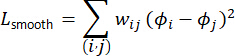
- Add both terms to the training objective.
- Compute band alignment loss:
2. Initialize Multi-Scale GNN Modules
- Define node embedding dimension = 128.
- Define edge embedding dimension = 64.
- Use four message-passing layers per scale.
- Use ReLU activation. Initialize weights using Xavier initialization.
- Implement Message Passing
- Implement edge update function as a multilayer perceptron (MLP).
- Implement node update function as a multilayer perceptron (MLP).
- Perform same-scale aggregation. Apply cross-scale attention-based fusion using Q/K/V projections.
NOTE: Ensure consistent embedding dimensionality across scales before fusion.
3. Quantum-Informed Modeling
- Define GNN-Parameterized Hamiltonian
- Replace explicit DFT Hamiltonian with:
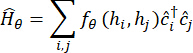
- Enforce Hermiticity:
fθ(hi,hj) = fθ(hj,hi)* - Truncate interactions beyond predefined graph distance.
- Replace explicit DFT Hamiltonian with:
- Define Physics-Constrained Loss
- Use:
![Static equilibrium equation, Lp=λ1||Hθψ−Erefψ||²+λ2Tr[(Hθ−Href)²], mathematical formula.](/files/ftp_upload/70059/70059eq8.jpg "figure-protocol-3")
- Tune λ parameters using validation set.
- Use:
- Enforce Physical Constraints
- Project Hamiltonian to Hermitian space each iteration.
- Penalize conservation law violations. Clip gradients to norm ≤ 5.
4. Reinforcement Learning for Topology Evolution
- Define State and Action Space
- Represent device graph as state Gt .
- Define actions:
- Add edge
- Remove edge
- Modify connectivity.
- Apply action masking for illegal edits.
- Define Reward Function
rt = αIQE + βStability - γComplexity
Tune α, β, γ via validation. - Train Policy Network
- Use policy gradient:
∇θJ = E[∑∇θlog πθ(at∣st)At] - Set the discount factor γ to 0.99. Set the entropy coefficient to 0.02 and anneal during training. Use the Adam optimizer with a learning rate of 1 × 10⁻4 and weight decay of 1 × 10⁻5.
- Use a batch size of 32. Train for 250–300 epochs and apply early stopping based on validation convergence.
- Use policy gradient:
5. Multi-Objective Optimization
- Formulate constrained objective. Apply the augmented Lagrangian.
- Generate Pareto frontier. Retain non-dominated solutions.
6. Transfer Learning
- Pre-train atomic GNN on energy prediction task. Save weights.
- Fine-tune on mesoscopic and device tasks with reduced learning rate (1×10⁻5). Evaluate MAE and R2.
7. COMSOL Multiphysics Validation
- Import AI-Designed Geometry
- Export device topology as CAD file.
- Import into COMSOL Multiphysics.
- Configure Simulation
- Use frequency-domain electromagnetic solver. Use semiconductor drift–diffusion solver.
- Use stationary thermal solver. Apply perfectly matched layers, ohmic contacts, and realistic excitation wavelengths.
- Extract Metrics
- Measure optical absorption efficiency, internal quantum efficiency, electric-field enhancement, and peak temperature rise.
- Average results across excitation conditions.
8. Scalability Testing
- Increase graph size up to 106 nodes. Measure runtime and memory usage.
- Enable spectral coarsening, sparse adjacency, mixed precision, and distributed GPU training.
9. Statistical Evaluation
- Run three independent training seeds.
- Report mean ± standard deviation, MAE, RMSE, and R2.
- Use identical splits and hyperparameters for baseline comparison.
10. Data and Code Archiving
- Save trained models. Archive datasets.
- Provide scripts for graph construction, training, and COMSOL validation.
Access restricted. Please log in or start a trial to view this content.
Results
The proposed multi-scale GNN-reinforcement learning framework was evaluated on 120,000 atomic graphs, 35,000 mesoscopic graphs, and 12,000 device-level graphs. Data were split at the device level into 70% training, 15% validation, and 15% testing sets. All reported values represent mean ± standard deviation across three independent runs using different random seeds. Baseline methods included SchNet, DimeNet++, physics-informed neural networks (PINNs), generative topology optimization, and a physics-only solver baseline. ...
Access restricted. Please log in or start a trial to view this content.
Discussion
This study presents a hierarchical, physics-informed graph-based framework for autonomous nanoelectronic and optoelectronic device design. The Results demonstrate that the method achieves competitive energy prediction accuracy, stable reinforcement-learning-driven topology evolution, constraint satisfaction, and physically validated improvements in device performance. The following discussion focuses on critical procedural elements, methodological considerations, limitations, contextual significance, and future extension...
Access restricted. Please log in or start a trial to view this content.
Disclosures
The author declares no conflicts of interest.
Acknowledgements
The authors have no acknowledgements.
Access restricted. Please log in or start a trial to view this content.
Materials
| Name | Company | Catalog Number | Comments |
|---|---|---|---|
| Computational & Modeling Software | |||
| JAX / Haiku | N/A | 0.3.0+ | |
| LAMMPS | N/A | - | |
| LUMERICAL / MEEP | N/A | - | |
| OpenAI Gym / Gymnasium | N/A | - | |
| Python | N/A | 3.8+ | |
| PyTorch / PyTorch Geometric | N/A | 1.9.0+ / 2.0+ | |
| Quantum ESPRESSO | N/A | 6.7+ | |
| Data & Datasets | |||
| DFT Simulation Database | N/A | Custom | |
| Generated Nanoelectronic Graphs | N/A | ~10,000 graphs | |
| Materials Project / OQMD | N/A | Public API | |
| Hardware & Infrastructure | |||
| Data Storage | N/A | NVMe SSDs | |
| High-Performance Computing (HPC) Cluster | N/A | CPU Nodes | |
| NVIDIA GPU Cluster | N/A | A100 / V100 / H100 | |
| Key Algorithms & Model Components | |||
| Adam / AdamW Optimizer | N/A | PyTorch Native | |
| Graph Attention Network (GAT) | N/A | Custom (PyTorch) | |
| Graph Variational Autoencoder (GVAE) | N/A | Custom (PyTorch) | |
| Message Passing Neural Network (MPNN) | N/A | Custom (PyTorch) | |
| Policy Gradient (e.g., PPO) | N/A | Custom (Stable-Baselines3) | |
| Machine Learning & Optimization Libraries | |||
| NetworkX | N/A | 2.6+ | |
| NumPy | N/A | 1.24+ | |
| Optuna | N/A | 2.0+ | |
| Scikit-learn | N/A | 1.0+ | |
| Stable-Baselines3 / Ray RLLib | N/A | - | |
| Physical & Mathematical Models | |||
| Augmented Lagrangian Method | N/A | Custom (Python) | |
| Composite Reward Function (rt) | N/A | Custom (Python) | |
| Parameterized Hamiltonian (Hθ) | N/A | Custom (PyTorch) | |
| Spectral Graph Coarsening | N/A | Custom (Scikit-learn) |
References
- Ekström Kelvinius, F., Armiento, R., Lindsten, F. ` Graph-based machine learning beyond stable materials and relaxed crystal structures. Physical Review Materials. 6 (3), 033801(2022).
- Merchant, A., et al. Scaling deep learning for materials discovery. Nature. 624 (7990), 80-85 (2023).
- Opanin Gyamfi, E., Qin, Z., Mantebea Danso, J., Adu-Gyamfi, D. Hierarchical Graph Neural Network: A Lightweight Image Matching Model with Enhanced Message Passing of Local and Global Information in Hierarchical Graph Neural Networks. Information. 15 (10), 602(2024).
- Hayes, C. F., et al. A practical guide to multi-objective reinforcement learning and planning. Autonomous Agents and Multi-Agent Systems. 36 (1), 26(2022).
- Luo, S., Li, T., Wang, X., Faizan, M., Zhang, L. High-throughput computational materials screening and discovery of optoelectronic semiconductors. Wiley Interdisciplinary Reviews: Computational Molecular Science. 11 (1), e1489(2021).
- Ilyas, N., et al. Nanostructured materials and architectures for advanced optoelectronic synaptic devices. Advanced Functional Materials. 32 (15), 2110976(2022).
- Pham, P. V., et al. 2D heterostructures for ubiquitous electronics and optoelectronics: principles, opportunities, and challenges. Chemical Reviews. 122 (6), 6514-6613 (2022).
- Krishnamoorthy, U., Balasubramani, S. Intelligent Nanomaterial Image Characterizations-A Comprehensive Review on AI Techniques that Power the Present and Drive the Future of Nanoscience. Advanced Theory and Simulations. 7 (12), 2400479(2024).
- Zhang, S., et al. The rise of AI optoelectronic sensors: From nanomaterial synthesis, device design to practical application. Materials Today Physics. 27, 100812(2022).
- Lay-Ekuakille, A., et al. Optoelectronic and nanosensors detection systems: A review. IEEE Sensors Journal. 21 (11), 12645-12653 (2021).
- Liu, W., et al. Ultra-compact multi-task processor based on in-memory optical computing. Light: Science & Applications. 14 (1), 134(2025).
- Wang, H., et al. Two-photon polymerization lithography for optics and photonics: fundamentals, materials, technologies, and applications. Advanced Functional Materials. 33 (39), 2214211(2023).
- Datye, I. M., Daus, A., Grady, R. W., Brenner, K., Vaziri, S., Pop, E. Strain-enhanced mobility of monolayer MoS2. Nano Letters. 22 (20), 8052-8059 (2022).
- Ma, J., et al. Prediction of high photoconversion efficiency and photocatalytic water splitting in vertically stacked TMD heterojunctions MX 2/WS 2 and MX 2/MoSe 2 (M= Cr, Mo, W; X= S, Se, Te). Journal of Materials Chemistry A. 13 (13), 9312-9322 (2025).
- Ren, K., et al. Sn) monolayers with ultrahigh carrier mobility: potential photocatalysts for water splitting. The Journal of Physical Chemistry C. 127 (43), 21006-21014 (2023).
- Shi, X., et al. Sumanene Monolayer of Pure Carbon: A Two-Dimensional Kagome-Analogy Lattice with Desirable Band Gap, Ultrahigh Carrier Mobility, and Strong Exciton Binding Energy. Small. 18 (40), 2203274(2022).
- Gao, S. Y., Zheng, Y. F., He, S. Q., Fang, H., Zhang, Y. Y. Sn9C15 monolayer with desirable bandgap, high carrier mobilities, and broadband light absorption for photovoltaic devices. The Journal of Chemical Physics. 162 (13), 134701(2025).
- Das, R. R., Chowdhury, A., Chakraborty, A. Parametric analysis on DC and analog/linearity response of multi-channel FinFET (Mch-FinFET) with spacer engineering. Analog Integrated Circuits and Signal Processing. 119 (1), 1-13 (2024).
- Indhur, V., et al. Dielectric Material and Thermal Optimization in Sidewall Spacer Design for Junctionless Nanosheet FETs at Sub-5 nm Technology Node: An Insight into Device and Circuit Performance. ECS Journal of Solid State Science and Technology. 13 (10), 103007(2024).
- Goar, V., Yadav, N. S. Foundations of machine learning. Intelligent Optimization Techniques for Business Analytics. , 25-48 (2024).
- Tapeh, A. T. G., Naser, M. Z. Artificial intelligence, machine learning, and deep learning in structural engineering: a scientometrics review of trends and best practices. Archives of Computational Methods in Engineering. 30 (1), 115-159 (2023).
- Javaid, M., Haleem, A., Singh, R. P., Suman, R., Rab, S. Significance of machine learning in healthcare: Features, pillars and applications. International Journal of Intelligent Networks. 3, 58-73 (2022).
- Wang, X., et al. Machine learning for risk and resilience assessment in structural engineering: Progress and future trends. Journal of Structural Engineering. 148 (8), 03122003(2022).
- A Detailed View on industrial Safety and Health Analytics using Machine Learning Hybrid Ensemble Techniques. Rathor, K., et al. 2022 International Conference on Edge Computing and Applications (ICECAA), , 1166-1169 (2022).
- Singla, A. Graph Neural Networks: Advances in Representation Learning for Structured Data Analysis). Shodh Sagar Journal of Artificial Intelligence and Machine Learning. 1 (2), 31-36 (2024).
- Ademovic Tahirovic, A., et al. Petri graph neural networks advance learning higher order multimodal complex interactions in graph structured data. Scientific Reports. 15 (1), 1-17 (2025).
- Paul, S. G., et al. A systematic review of graph neural network in healthcare-based applications: Recent advances, trends, and future directions. IEEE Access. 12, 15145-15170 (2024).
- Liu, L., Yang, F., Shang, L., Zeng, X. GNN-Cap: Chip-Scale Interconnect Capacitance Extraction Using Graph Neural Network. IEEE Transactions on Computer-Aided Design of Integrated Circuits and Systems. 43 (4), 1206-1217 (2023).
- Saxena, S., et al. GNN-assisted phase space integration with application to atomistics. Mechanics of Materials. 182, 104681(2023).
- Shen, Y., et al. The trend of 2D transistors toward integrated circuits: scaling down and new mechanisms. Advanced Materials. 34 (48), 2201916(2022).
- Lopes, P. A., Santos, B. C., de Almeida, A. T., Tavakoli, M. Reversible polymer-gel transition for ultra-stretchable chip-integrated circuits through self-soldering and self-coating and self-healing. Nature Communications. 12 (1), 4666(2021).
- Rapp, M., et al. MLCAD: A survey of research in machine learning for CAD keynote paper. IEEE Transactions on Computer-Aided Design of Integrated Circuits and Systems. 41 (10), 3162-3181 (2021).
- Sun, X., Tian, G., Yang, S., Yuan, P., Zhang, S. Asymptotically optimal circuit depth for quantum state preparation and general unitary synthesis. IEEE Transactions on Computer-Aided Design of Integrated Circuits and Systems. 42 (10), 3301-3314 (2023).
- Asif, N. A., et al. Graph neural network: A comprehensive review on non-euclidean space. IEEE Access. 9, 60588-60606 (2021).
- Singh, A. K., Palanisamy, R., Jain, A. K. Efficient nanoscale device modeling using artificial neural networks with TensorFlow and Keras libraries in Python. Signal Processing with Python: A practical approach. , 7-1 (2024).
- Fischetti, M., Gaddemane, G., Gopalan, S., Van de Put, M. L., Vandenberghe, W. The Future of Nanoelectronics Devices from a Theoretical Point of View: The Search for New Channel Materials. ECS Transactions. 111 (1), 81(2023).
- Wang, A., Chen, R., Yun, Y., Xu, J., Zhang, J. Review of Ferroelectric Materials and Devices toward Ultralow Voltage Operation. Advanced Functional Materials. 35 (7), 2412332(2025).
- Zhang, Y. F., et al. Emerging Multifunctionality in 2D Ferroelectrics: A Theoretical Review of the Interplay With Magnetics, Valleytronics, Mechanics, and Optics. Advanced Functional Materials. 34 (51), 2410240(2024).
- Raut, P., Nanda, U., Panda, D. K. Recent trends on junction-less field effect transistors in terms of device topology, modeling, and application. ECS Journal of Solid State Science and Technology. 12 (3), 031010(2023).
- D'agostino, S., et al. DenRAM: neuromorphic dendritic architecture with RRAM for efficient temporal processing with delays. Nature Communications. 15 (1), 3446(2024).
- Dalgaty, T., et al. Mosaic: in-memory computing and routing for small-world spike-based neuromorphic systems. Nature Communications. 15 (1), 142(2024).
- Huynh, N., et al. The use of generative adversarial network and graph convolution network for neuroimaging-based diagnostic classification. Brain Sciences. 14 (5), 456(2024).
- Abadal, S., et al. Computing graph neural networks: A survey from algorithms to accelerators. ACM Computing Surveys (CSUR). 54 (9), 1-38 (2021).
- Mondal, S., et al. A unified engine for accelerating GNN weighting/aggregation operations, with efficient load balancing and graph-specific caching. IEEE Transactions on Computer-Aided Design of Integrated Circuits and Systems. 42 (12), 4844-4857 (2022).
- Tang, E., et al. Graph-OPU: A Highly Flexible FPGA-Based Overlay Processor for Graph Neural Networks. ACM Transactions on Reconfigurable Technology and Systems. 17 (4), 1-33 (2024).
- Galván, E., Mooney, P. Neuroevolution in deep neural networks: Current trends and future challenges. IEEE Transactions on Artificial Intelligence. 2 (6), 476-493 (2021).
- Duan, K., et al. A comprehensive study on large-scale graph training: Benchmarking and rethinking. Advances in Neural Information Processing Systems. 35, 5376-5389 (2022).
- Gundla, K., Martha, S., Panigrahy, A. K. Toward Explainable AI in Satellite Imagery: A ResNet-50-Based Study on EuroSAT Classification. IEEE Access. 13, 165900-165908 (2025).
- Jain, A., Panigrahy, A. K., Saini, S., Kumar Bansal, A., Nayak Bhukya, M. Chef-Based Optimization Algorithm (CBOA)-Based Global Peak Power Tracking Scheme for PV System. IEEE Access. 13, 156246-156257 (2025).
- Ahmed, M. I., Kumar, A. N., Prasanna, B. L., Panigrahy, A. K. Dual spacer-engineered FinFETs with enhanced electrostatic control at nanoscale. Microsystem Technologies. 31 (12), 3747-3754 (2025).
- Panigrahy, A. K., et al. Development and comparative analysis of a GAA nanosheet FET across diverse space charge region materials for nanoscale applications. Micro and Nanostructures. 206, 208239(2025).
Access restricted. Please log in or start a trial to view this content.