This protocol defines the simulation, design, testing, and fabrication of a low-cost, coplanar waveguide-fed (CPW) Ultra-Wide-Band (UWB) antenna for radio-frequency energy harvesting (RFEH) across multiple communication bands.
A subscription to JoVE is required to view this content. Sign in or start your free trial.
Method Article
Coplanar Waveguide Fed Ultra-Wide-Band Monopole Antenna for Radio Frequency Energy Harvesting Applications
In This Article
Summary
Abstract
The RFEH based on wireless charging is a promising technology for powering low-energy Internet-of-Things (IoT) devices; however, its efficiency is still limited by antenna design and impedance matching. In this work, a printed antenna suitable for RFEH is developed with a CPW feed. The antenna is composed of a semicircular fractal curve, similar to a fig leaf tree radiating patch, with rectangular notches to be fabricated on an FR4 low-cost substrate. It has an operational bandwidth of 700 MHz to 3 GHz, covering key communication bands, including GSM, WLAN, ISM, and Wi-Fi applications. Numerical simulations were performed using computational electromagnetic modeling software. The experimental work demonstrated the suitability of this antenna for stable omnidirectional radiation patterns and successful RF-to-DC conversion efficiencies at the five target frequencies, including 850 MHz, 900 MHz, 1800 MHz, 1900 MHz, and 2400 MHz. The antenna shows potential for powering low-energy IoT devices in ambient RF conditions. The proposed work aims to compare the measured and simulated results. Lastly, the numerical and experimental results are compared and show remarkable agreement.
Introduction
Recent developments in wireless communication systems such as 5G, 6G, and IoT1,2,3,4 have resulted in an increasing demand for efficient RFEH solutions. Urban environments are filled with ambient RF signals from cellular base stations, Wi-Fi access points, and broadcast transmitters, which makes them a suitable parasitic power source for low-energy electronic devices5,6,7. In particular, UWB antennas, such as monopole configurations, are well-suited for RF energy harvesting applications, mainly due to their wide instantaneous bandwidth, simple planar geometry, and easy integration with rectifier circuits8. The feeding CPW structure offers further benefits, including better impedance matching, reduced parasitic radiation from the feed line, and easier fabrication without backside ground planes9.
Although several UWB antennas have been reported for general wireless communications, many are designed for signal fidelity or pulse preservation, rather than wideband RF-to-DC energy conversion in specific commercial frequency bands10,11. Other recent directions include compact high-gain designs12, rectenna-specific antennas with integrated matching networks13 and tunable structures14 for cognitive radio. However, these techniques typically rely on multilayer substrates, complex etching processes, or narrowband resonators, which limit their use in ambient multi-band harvesting scenarios. Compared to the prior art, the present work provides four practical improvements in direct comparison, namely: (1) A fully printable, single-layer FR4 design that reduces the fabrication cost and complexity relative to multilayer or high-frequency laminate solutions15,16; (2) An operational bandwidth from 700 MHz up to 25 GHz, covering the GSM (Global System for Mobile Communications), DCS, PCS, and Wi-Fi bands simultaneously, whereas many prior antennas cover fewer or discontinuous bands17,18; (3) Explicit experimental validation in a harvesting setup (RF-to-DC efficiency measurement across five discrete frequencies) rather than only S11 or gain characterization19,20; (4) A CPW-fed semicircular geometry with rectangular notches that achieves wideband matching without via holes or defected ground structures, easing reproducibility in low-resource settings21.
The technology of RF ambient harvesting is promising, but practical realizations suffer from well-documented constraints. The power density of ambient RF fields in urban environments is usually in the range of 0.1 µW/cm2 to 1 µW/cm2, corresponding to received power levels on the order of -30 dBm to -10 dBm for a compact antenna22,23. Therefore, we aim for an input RF power level of -20 dBm in this work for harvesting evaluation, within the scope of moderate-distance ambient scenarios. Here, “low-energy devices” based IoT sensors, wearables, and wireless nodes that require an average DC power of between 100 µW and 1 mW24. One known limitation, which we expect here and revisit in the Discussion section, is the use of a FR4 substrate with a loss tangent (tan δ = 0.025) that degrades efficiency above approximately 2 GHz; however, the target bands (up to 2.4 GHz) and the extended UWB range are still suitable for harvesting due to the wide impedance matching25.
A CPW-fed UWB monopole antenna with a semicircular patch and two symmetrical rectangular notches is proposed, specifically designed for RF energy harvesting in the GSM at 850/900 MHz, DCS at 1800 MHz, PCS at 1900 MHz, and Wi-Fi at 2400 MHz frequency bands. The novelty lies in its geometric simplicity, experimentally validated broad bandwidth, and direct demonstration of RF-to-DC conversion on a harvesting evaluation board. To the best of our knowledge, a low‑cost, printable UWB monopole tailored specifically for multi‑band energy harvesting across these five frequencies, using a commercial rectifier, has remained underexplored26,27,28.
Access restricted. Please log in or start a trial to view this content.
Protocol
The consumables, equipment, and software used are listed in the Table of Materials.
1. Antenna design and simulation
- Substrate selection and initial geometry
- Select an FR4 substrate with a dielectric constant (εr) of 4.3, loss tangent (tan δ) of 0.025, and dimensions of 125 mm × 95 mm × 1.6 mm as seen in Figure 1.
- Open the electromagnetic field simulation software. Create a new project and set units to millimeters.
- Define the substrate material using the built-in FR4 model.
- Draw a semicircular copper patch (radius = 40 mm) and a rectangular ground plane (95 mm × 40 mm) on the same layer.
- Insert a 50 Ω CPW feed line (width = 3 mm, gap = 0.5 mm) connected to the patch.
- Geometry optimization for UWB performance
- Add two rectangular notches (width = 3 mm, depth = 5 mm) symmetrically on the lower edge of the semicircular patch.
- Flare the CPW feed line at a 20° angle to improve impedance matching.
- Run a parametric sweep varying notch width (1–5 mm), notch depth (2–10 mm), and flare angle (10°–30°).
- Set the frequency range from 0.5 MHz to 3 GHz. Use the Time Domain Solver with open boundary conditions.
- Define a discrete port at the feed line. Add a frequency monitor for far-field radiation. The antenna surface current is evaluated as seen in Figure 2.
- Simulate and check S11. Iterate until S11 < -10 dB from 0.5 MHz to 3 GHz.
- Cross-verification with alternative software
- Extract the final antenna design geometry as a .SAT file.
- Run the finite-element EM simulation software after importing the proposed model.
- Assign the same material properties and boundary conditions.
- Run the Finite Element Method (FEM) technique. Set the frequency sweep from 0.5 MHz to 3 GHz with 2001 points.
- Comparing the S11 spectra and the radiation patterns from the CST solver to confirm consistency.
2. Antenna fabrication
- PCB layout preparation
- From CST, export the final design to a Gerber file for both top and back Layers.
- Run the Gerber file in a PCB design software (KiCad) and confirm the dimensions.
- Produce NC drill file for SMA holes.
- Photolithography process
- Clean the FR4 substrate with isopropyl alcohol and dry it well.
- Cover the dry photoresist films onto the considered substrate at 115 °C.
- Print the antenna layer on a transparent film using a high-resolution printer.
- Press the film mask with alignment on the substrate to be exposed to the UV light for 50 s.
- Developing the substrate in a sodium carbonate solution of 1.5% w/v must be for 70 s.
- Rinse with deionized distilled water and dry with fresh air.
- Etching and finishing
- Etch the exposed copper using ferric chloride solution (45 °C) for 6–12 min.
- Stop etching after removing the unwanted copper.
- Strip the residual photoresist with acetone.
- Solder the SMA connector to the proposed CPW feed line using lead-free solder as shown in Figure 3.
- Check the antenna under a microscope for imperfections.
3. Experimental measurements and characterizations
- S11 spectra measurement
- Link the antenna to the power spectrum analyzer through a 50 Ω flexible coaxial cable.
- Apply with a full two-port calibration process using an electronic calibration kit.
- Perform the frequency range from 0.5 MHz to 3 GHz, with 2001 points and an IF bandwidth of 1 kHz.
- Apply averaging over 10 sweeps to minimize noise.
- Measure S11 and export data as a .csv file.
- Radiation pattern measurement
- Place the antenna in an anechoic chamber (4 m × 4 m × 4 m) on a motorized positioner.
- Align the antenna’s phase center with the rotation axis.
- Use a standard gain horn antenna as the transmitter, placed 3 m away.
- Set the signal generator to each target frequency (850, 900, 1800, 1900, 2400 MHz) with 0 dBm output power.
- Rotate the antenna under test in 5° increments and record received power.
- Normalize patterns to the maximum gain and plot in dB.
- RF energy harvesting evaluation
- Connect the antenna to a commercial RF harvesting evaluation board.
- Apply an input RF signal at each target frequency with -20 dBm power.
- Measure the DC output voltage across a 1 kΩ load resistor using a digital multimeter.
- Calculate RF-to-DC efficiency using:
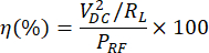
- Repeat measurements three times and average the results.
Access restricted. Please log in or start a trial to view this content.
Results
Figure 1 shows the geometry of the proposed antenna, which consists of a semicircular radiating patch with two symmetrical rectangular notches and a CPW feed line. The surface current distribution at 1.8 GHz, as shown in Figure 2, confirms the strong current concentration along the feed line and the lower edges of the patch, consistent with the fundamental resonant mode responsible for the wideband impedance matching. Figure...
Access restricted. Please log in or start a trial to view this content.
Discussion
A simple modified monopole structure with two symmetrical rectangular notches is proposed to design a wideband CPW-fed UWB monopole antenna with a working frequency range from 700 MHz to 25 GHz. This section offers a critical methodological interpretation of the protocol, discusses optimization decisions and troubleshooting considerations, compares the design with existing approaches, and explores future applications and developments.
Key protocol steps that affect performance and repr...
Access restricted. Please log in or start a trial to view this content.
Disclosures
The authors declare no competing interests.
Acknowledgements
The authors thank the International Applied and Theoretical Research Center (IATRC) for technical support.
Access restricted. Please log in or start a trial to view this content.
Materials
| Name | Company | Catalog Number | Comments |
|---|---|---|---|
| Acetone (Photoresist Stripper) | Fisher Chemical | A18-4 | Purity ≥ 99.5% |
| Ansys HFSS 2022 R2 | Ansys Inc. | Version: 2022 R2, Solver: Finite Element Method (FEM) | |
| Compact Anechoic Chamber | ETS-Lindgren | Model 5300 | Internal dimensions: 4 m × 4 m × 4 m, Frequency range: 700 MHz – 40 GHz |
| Copper Cladding | Generic PCB copper foil | Thickness = 35 µm (1 oz), Adhesion = 1.5 N/mm² | |
| CST Studio Suite 2022 | Dassault Systèmes | Version: 2022, Solver: Finite Integration Technique (FIT) | |
| Digital Multimeter (DMM) | Keysight | 34461A | DC Voltage range: 0–100 V, Accuracy: ±0.0035% |
| Digital USB Microscope | Celestron | 44308 | Magnification: 10x–200x, LED illumination |
| Dry Photoresist Film | ORCAL | 925 | Thickness = 1.2 mil, Lamination temperature = 110 °C |
| Electronic Calibration Module (ECal) | Keysight | N4691B | Frequency range: 10 MHz – 26.5 GHz, 2-port |
| Ferric Chloride Etchant | MG Chemicals | 415 | Concentration = 40–42 °Baumé, Temperature = 40 °C |
| FR4 Epoxy Laminate | Isola Group | FR408 | εr = 4.3, tan δ = 0.025, Thickness = 1.6 mm, Dimensions = 125 mm × 95 mm |
| Hot Roll Laminator | GBC | H65 | Temperature range: 80–140 °C, Speed: 0.5–3 m/min |
| Isopropyl Alcohol (Cleaning Agent) | Sigma-Aldrich | 34863 | Purity = 99.9% |
| KiCad 7.0 | KiCad EDA | Open-source, used for Gerber file verification | |
| Lab Coat | Medline | DYNA23100 | 65% polyester / 35% cotton |
| Lead-Free Solder Wire | Kester | 245 No-Clean | Diameter = 0.8 mm, Composition: Sn96.5/Ag3.0/Cu0.5 |
| Motorized Antenna Positioner | Orbit | FR-959 | Azimuth rotation: 0–360°, Elevation: ±180°, Step resolution: 0.1° |
| Nitrile Gloves | Kimberly-Clark | Kimtech | Powder-free, thickness: 5 mil |
| PCB Drill (for connector holes) | Proxxon | MICROMOT 50/E | Drill bit diameter: 1.2 mm (for SMA mounting holes) |
| Powercast P2110B Evaluation Board | Powercast Corporation | Integrated matching network, Schottky rectifier, and storage capacitor | |
| Precision Tweezers | Excelta | 225A-SF | Anti-magnetic, stainless steel |
| RF Signal Generator | Keysight | N5172B | Frequency range: 9 kHz – 13.6 GHz, Output power: +23 dBm |
| Safety Goggles | Uvex | Stealth | Anti-fog, UV protection |
| SMA Cable, 50 Ω | Huber+Suhner | Sucoflex 104 | Length = 1 m, Frequency range: DC – 26.5 GHz, Insertion loss < 0.5 dB at 18 GHz |
| SMA Female PCB Edge Mount Connector | Amphenol | 901-9871 | 50 Ω, Frequency range: DC–18 GHz |
| Sodium Carbonate (Developer) | Sigma-Aldrich | 451614 | Concentration = 1% w/v in deionized water |
| Standard Gain Horn Antenna | ETS-Lindgren | 3164-05 | Frequency range: 800 MHz – 5 GHz, Gain: 6–12 dBi |
| UV LED Exposure System | M&R | Saturn 2 | Wavelength: 365 nm, Power: 120 W |
| Vector Network Analyzer (VNA) | Keysight | N5222B | Frequency range: 10 MHz – 26.5 GHz, Ports: 2 |
References
- Al-Saegh AM, et al. Channel quality predictions assisted by new algorithms for high throughput satellite and 5G systems. Sci Rep. 2025;15:34649.
- Elwi TA, et al. A beam-split and gain-enhanced patch antenna using metamaterial superstrate for wireless communications. Informacije MIDEM. 2025;55(3):1-10.
- Taher F, et al. Novel antenna-based metamaterial structure with slotted and parasitic patches for 5G sub-6 GHz applications. J Adv Res Appl Sci Eng Technol. 2025;65(2):143-152.
- Elwi TA, et al. On the performance of a photonic reconfigurable electromagnetic band gap antenna array for 5G applications. IEEE Access. 2024;12:1-12.
- Hamad AR, et al. Rectenna design optimized by binary genetic algorithm for hybrid energy harvesting applications across 5G sub-6 GHz band. Radio Sci. 2025;60(6):e2024RS008154.
- Alnaiemy Y, et al. A further realization of binary genetic algorithm to design a dual frequency band rectenna for energy harvesting in 5G networks. DJES. 2025;18(2):203-214.
- Alsudani M, Ozturk T, Oleiwi TA. Performance of CRLH-TL-Hilbert structure inspired antenna loaded with AMC reflector for wireless applications. J Vis Exp. 2026;(231):e70367.
- Al-Rawe TSA, et al. A dual-band high-efficiency fractal rectenna for RF energy harvesting systems. In: 2023 5th International Congress on Human-Computer Interaction, Optimization and Robotic Applications (HORA); 2023. p.1-6.
- Almizan H, et al. Novel metasurface based microstrip antenna design for gain enhancement RF harvesting. Infocommunications J. 2023;15(1):2-8.
- Elwi TA. A systematic study on the metamaterial microstrip antenna design for self-powered wireless systems. 2024: DOI:10.1049/PBCE124E_ch5.
- Alaukally MNN, et al. Miniaturized flexible metamaterial antenna of circularly polarized high gain-bandwidth product for radio frequency energy harvesting. Int J Commun Syst. 2022;35(3):e5024.
- Almizan H, et al. Circularly polarized, wide-range coverage azimuth and elevation angles microstrip antenna for RF harvesting. J Eng Sustain Dev. 2020;24:191-198.
- Elwi TA, et al. Further realization of a flexible metamaterial-based antenna on indium nickel oxide polymerized palm fiber substrates for RF energy harvesting. Int J Microw Wirel Technol. 2021;13(1):67-75.
- Elwi TA. A further realization of a flexible metamaterial-based antenna on nickel oxide polymerized palm fiber substrates for RF energy harvesting. Wirel Pers Commun. 2020;115(2):1623-1634.
- Elwi TA, et al. Novel miniaturized folded UWB microstrip antenna-based metamaterial for RF energy harvesting. Int J Commun Syst. 2020;33(6):e4305.
- Elwi TA, et al. Hilbert metamaterial printed antenna based on organic substrates for energy harvesting. IET Microw Antennas Propag. 2019;13(12):2185-2192.
- Elwi TA. Novel UWB printed metamaterial microstrip antenna based organic substrates for RF energy harvesting applications. AEU Int J Electron Commun. 2019;101:44-53.
- Elwi TA, et al. A UWB monopole antenna design based RF energy harvesting technology. In: 2018 Third Scientific Conference of Electrical Engineering (SCEE); 2018: DOI:10.1109/SCEE.2018.8684112.
- Jassim YA, et al. 10 GHz printed circuit antenna for wireless power transfer applications. In: 2023 5th International Congress on Human-Computer Interaction, Optimization and Robotic Applications (HORA); 2023: DOI:10.1109/HORA58378.2023.10156795.
- Abbood HT, et al. A dual band rectenna designed with binary coding technique of genetic algorithm. In: 2025 5th International Conference on Artificial Intelligence and Signal Processing (AISP); 2026: DOI:10.1109/AISP68263.2025.11396314.
- Noori NM, et al. IoT borders security technology with aid of VANET machine learning applications. In: 2024 4th International Conference on Artificial Intelligence and Signal Processing (AISP); 2024: DOI:10.1109/AISP61711.2024.10870694.
- Al-Asady R, et al. A modern RIS design based AI driven for cooperative relay networks. Iraqi J Inf Commun Technol. 2025;8(3):73-82.
- Elwi TA, et al. IAE-CRP: Improved ant optimization with ECC-based clustered routing protocol for wireless sensor network. Iraqi J Inf Commun Technol. 2026;9(1):30-43.
- Ismail MM, et al. Frequency reconfigurable using CRLH for 5G sub-6 GHz wireless application. Iraqi J Inf Commun Technol. 2025;8(3):62-72.
- Jwair MH, et al. Circularly shaped metamaterial fractal reconfigurable antenna for 5G networks. Iraqi J Inf Commun Technol. 2023;6(3):65-75.
- Hadi SM, Abdullah O, Al-Saegh AM, et al. Uncertainty-calibrated indoor localization with Sinkhorn contrastive pretraining and MDN-transformer using beamforming feedback. Research Square. 2026: https://doi.org/10.21203/rs.3.rs-9128192/v1.
- Alaukally MNN, Ilyas M, Oleiwi TA. Fabrication and testing of an optically controlled microwave sensor for urea level detection in urine. J Vis Exp. 2026;(231):e70483.
- Al-Attar S, Alibakhshikenari M, Qasaymeh YM, et al. A reconfigurable MTM-EMBG MIMO antenna array with solar panel integration for sustainable 5G networks. Sci Rep. 2026: https://doi.org/10.1038/s41598-026-48125-x.
Access restricted. Please log in or start a trial to view this content.