This protocol describes heterodyne-detected tapping-mode photothermal atomic force microscopy–infrared spectroscopy for nanoscale chemical characterization of semiconductor materials and devices, including infrared spectral acquisition and chemical mapping of patterned surfaces and process-related contaminants.
A subscription to JoVE is required to view this content. Sign in or start your free trial.
Method Article
Implementation of Heterodyne-Detected Tapping-Mode Photothermal Atomic Force Microscopy–Infrared Spectroscopy for Semiconductor Materials and Devices
In This Article
Summary
Abstract
Atomic force microscopy (AFM) is widely used to characterize the nanoscale electrical, magnetic, mechanical, thermal, electrochemical, and electromechanical properties of materials and devices; however, it does not directly provide chemical identification. In contrast, infrared (IR) spectroscopy probes chemical bonds through their vibrational signatures but is traditionally limited to micron-scale spatial resolution by optical diffraction. Photothermal AFM–IR spectroscopy (AFM–IR) combines AFM and IR spectroscopy to enable nanoscale chemical characterization by measuring localized photothermal expansion following IR absorption. This article presents a protocol for heterodyne-detected tapping-mode photothermal AFM–IR and its application to semiconductor materials and devices. The protocol describes instrument preparation, probe selection and tuning, AFM topography imaging, IR laser alignment and optimization, acquisition of localized IR spectra, and chemical mapping of selected vibrational modes. Particular emphasis is placed on practical implementation of tapping-mode AFM–IR for semiconductor characterization and factors that influence data quality, including probe selection, resonance tuning, and IR beam alignment. Representative examples demonstrate the use of AFM–IR to distinguish material composition in patterned structures, evaluate deposited materials on semiconductor substrates, and identify residual photoresist contamination following processing. The protocol enables acquisition of co-localized topographical and chemical information with nanoscale spatial resolution and illustrates how AFM–IR can be applied to characterization challenges encountered in semiconductor research and manufacturing. To assist new users, a brief overview of AFM–IR development and a comparison of commonly used IR sources and imaging modes are also provided.
Introduction
Advanced characterization methods play a vital role in semiconductor research, development, and manufacturing. Atomic force microscopy (AFM), which can be performed under ambient conditions, in a cleanroom environment, in an inert atmosphere glovebox, or under vacuum, is widely employed in the semiconductor industry. Available AFM modes combine nanoscale topographical mapping of semiconductor materials and devices with co-localized electrical, magnetic, mechanical, piezoelectric (i.e., electromechanical), and thermal measurements, including surface potential, electrical resistance, dopant profiling, and site-specific current–voltage (I–V) measurements1,2,3,4,5. However, despite its ability to provide a wealth of property information, AFM does not directly provide chemical-composition information. In contrast, infrared (IR) absorption spectroscopy probes the chemical bonds or phonon modes present in a sample but is traditionally limited to micron-scale spatial resolution because of the Abbe diffraction limit and the wavelength of mid-IR light (~2.5–25 µm or 400–4,000 cm−1)6,7,8. The development of photothermal AFM–IR6,7,8,9,10,11,12,13, which combines AFM with near-field IR microscopy and spectroscopy for nanoscale chemical identification, addresses this limitation7,8,14,15,16. AFM–IR accomplishes this by focusing a mid-IR (MIR) source onto a typically metal-coated nanoscale (~20 nm) AFM probe tip, enabling co-localized acquisition of AFM topography and IR spectroscopy data (Figure 1)6,7,8,11,15,16,17,18,19,20,21.
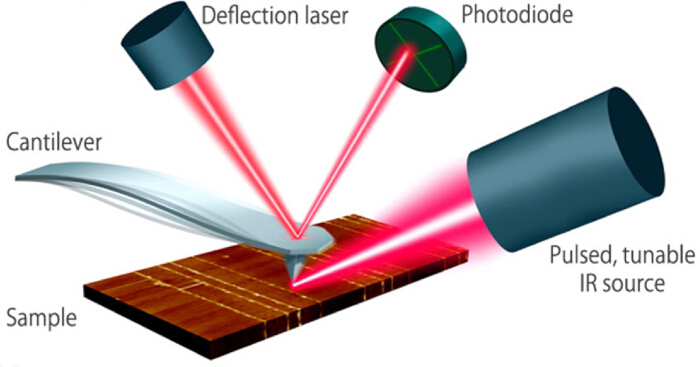
Figure 1. Schematic illustration of photothermal atomic force microscopy–infrared spectroscopy (AFM–IR). A focused pulsed infrared (IR) beam excites localized photothermal expansion of the sample surface. The resulting cantilever oscillation is detected using the AFM deflection laser and position-sensitive photodiode, enabling co-localized acquisition of sample topography and chemical information at the nanoscale. Adapted with permission from Figure 1A in Dazzi and Prater7. Copyright 2017 American Chemical Society. Please click here to view a larger version of this figure.
Initial implementations of AFM–IR utilized a broadband IR source, sometimes in combination with a specialized thermally sensitive probe rather than a standard AFM cantilever22,23. Researchers subsequently adopted pulsed IR sources24, which provide higher peak powers and, in the case of tunable repetition rates, enable resonance enhancement (RE) of the cantilever response to photothermal excitation of the sample11,15,25,26, resulting in detection sensitivities approaching the monolayer level21. The first AFM–IR system to demonstrate nanoscale IR resolution employed a free-electron laser and bottom-up evanescent-wave illumination through an IR-transmissive substrate9. Shortly thereafter, top-down illumination27 using a wavelength-tunable optical parametric oscillator (OPO)24,28 or tabletop laser source, such as a quantum cascade laser (QCL)11,21, was introduced10. This configuration forms the basis of most current commercial AFM–IR systems because top-down illumination simplifies sample preparation by eliminating the requirement for an IR-transmissive substrate and enables analysis of thicker samples7,8,15,16. Subsequent developments enabled acquisition of IR spectra at selected locations on a sample surface and chemical mapping of specific vibrational modes6,7,8,9,15,24,29,30,31,32. As a result, AFM–IR has been applied across a broad range of fields, including biology and drug delivery6,25,33,34,35,36,37, polymer characterization6,12,26,38,39, nanoparticle identification26,40,41,42,43, and semiconductor research7,44,45,46,47,48,49, with ongoing efforts focused on expanding the accessible wavelength range and, consequently, the variety of vibrational modes and material systems that can be investigated8,28,50.
Related techniques, such as IR scattering-type scanning near-field optical microscopy (IR s-SNOM)14,51,52,53,54,55,56,57,58,59,60,61 and tip-enhanced Raman scattering (TERS)62,63,64,65,66, detect elastically or inelastically scattered light, respectively. In contrast, AFM–IR uses the AFM probe cantilever to transduce and amplify, through the quality factor (Q factor) of the cantilever resonance, the photothermal expansion of the sample surface following IR excitation6,7,8,14,15,16,31,67. The resulting probe oscillation is detected by measuring the movement of the AFM deflection laser, which is reflected from the back of the cantilever, on the position-sensitive detector (Figure 1). Because this detection pathway is also used to measure changes in sample topography, AFM–IR requires a method to separate the topographical and IR absorption responses. This separation was initially achieved using contact-mode AFM. Following excitation of the sample by an IR pulse, the probe response to the sample’s photothermal expansion decays rapidly on a nanosecond-to-microsecond timescale, which is much faster than the millisecond-scale effective probe dwell time associated with AFM data acquisition at rates of a few kilohertz6,8,15,16,50,67. The resulting time-varying optical signal, or ringdown, at each data point (i.e., AFM image pixel) can be filtered through a frequency band-pass centered around the cantilever contact resonance frequency and Fourier transformed. The resulting amplitude is proportional to the localized photothermal response of the sample (Figure 2A, 2B)6,7,8,15,31,67,68. However, variations in sample stiffness can shift the probe contact resonance frequency, which may convolve the photothermal expansion signal with variations in the mechanical behavior of the sample surface. To improve the sensitivity of contact-mode AFM–IR, resonance-enhanced (RE) AFM–IR was developed. In this mode, the laser pulse repetition rate is tuned to match a contact resonance frequency of the probe, causing in-phase amplification of the cantilever mechanical resonance and converting the ringdown decay into a continuous-wave oscillation (Figure 2C, 2D)7,8,11,15,21. This approach substantially improves the signal-to-noise ratio (S:N) in proportion to the Q factor of the cantilever resonance8,15,16,21. The incorporation of a phase-locked loop (PLL) allows the cantilever resonance to be monitored continuously and the laser pulse repetition rate matched to the varying resonance frequency while the sample response is mapped at a selected IR wavenumber. This helps ensure that the measured RE AFM–IR signal remains proportional to the IR absorption coefficient of the vibrational mode, independent of variations in mechanical properties, and therefore contact resonance frequency, across the sample surface8,15,16,37,69.
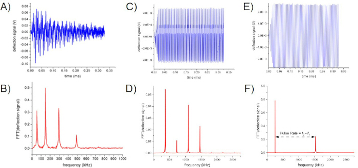
Figure 2. Representative time-domain and frequency-domain responses obtained using different AFM–IR operating modes. (A) Time-domain cantilever ringdown response following photothermal excitation of a sample during contact-mode AFM–IR. (B) Fast Fourier transform (FFT) of the ringdown signal in (a), showing multiple contact-resonance modes. (C) Time-domain response acquired during resonance-enhanced contact-mode AFM–IR using a soft cantilever (k = 0.3 N/m). (D) FFT of the resonance-enhanced signal showing amplification at the selected contact resonance (365 kHz), corresponding to the laser pulse repetition rate. Peaks at approximately 730, 1095, and 1460 kHz correspond to higher-order harmonics. (E) Time-domain tapping-mode AFM–IR signal acquired using a stiff cantilever (k = 40 N/m). (F) FFT of the tapping-mode AFM–IR response. Topography acquisition was performed using the drive resonance at approximately 250 kHz, while the photothermal response was detected at approximately 1.55 MHz using a heterodyne pulse repetition rate corresponding to the difference frequency (f₂ − f₁) of approximately 1.3 MHz. Panels (A, B) adapted with permission from Figure 3 in Mathurin et al.16 Copyright 2022 AIP Publishing. Please click here to view a larger version of this figure.
The next major advancement in AFM–IR technology was the implementation of heterodyne detection70, which enabled the combination of tapping-mode AFM with AFM–IR for imaging soft, sticky, or lightly adhered samples8,15,16,25,26,37,71. In tapping mode, also referred to as intermittent-contact mode, the probe is oscillated at or near a cantilever resonance frequency to induce intermittent contact with the sample surface, thereby reducing lateral forces and minimizing the potential for damage to the sample and/or probe. Compared with contact-mode operation, tapping mode is therefore particularly advantageous for samples that are mechanically soft, weakly adhered, or susceptible to surface modification during imaging8,15,16,25,26,37,71. In tapping-mode AFM–IR, the laser pulse repetition rate is set to the difference between two cantilever resonance frequencies, such that flaser = Δf = f2 − f1. One resonance frequency is used to acquire sample topography (ftap), while the second resonance frequency monitors the photothermal response (fdemod) arising from IR absorption (Figure 2E, 2F)8,15,16,71,72. Similar to resonance-enhanced contact-mode AFM–IR, a PLL can be used to maintain synchronization between the laser pulse repetition rate and Δf during scanning, compensating for small shifts in the cantilever resonance frequencies caused by variations in the tip-sample interaction potential across the surface8,16. The cantilever response (oscillation amplitude, Z) in heterodyne-detected tapping-mode AFM–IR depends on ftap, fdemod, Δf, and the Q factor of the selected demodulation resonance8,15,16,26,71:

Thus, when other factors are comparable (e.g., similar Q factors for f1 and f2), improved S:N can be achieved by using a stiffer probe, operating in tapping mode at the higher resonance frequency (i.e., ftap = f2), and demodulating the photothermal response at the lower resonance frequency (i.e., fdemod = f1). Beyond enabling analysis of soft, sticky, or lightly adhered samples, tapping-mode AFM–IR offers reduced sensitivity to variations in sample mechanical properties, approximately two-fold improved lateral resolution (~10 nm versus ~20 nm), and approximately 10–20-fold improved surface sensitivity relative to contact-mode implementations8,15,16,26,71.
In collaboration with academic and industry partners, tapping-mode AFM–IR has been used to evaluate deposition and material-removal processes on patterned wafers44,45, identify undesired nucleation sites44, detect residual photoresist45, and optimize processing conditions for contact pads in wide-bandgap semiconductor devices45. The protocol presented here describes heterodyne-detected tapping-mode AFM–IR and demonstrates its application for acquiring nanoscale IR spectra at selected locations, as well as for mapping the spatial distribution of chemical species through vibrational-mode imaging at fixed IR wavenumbers. Although AFM–IR can also provide information related to molecular orientation through polarization-dependent measurements8,16,73,74,75,76, those applications are beyond the scope of the present protocol and representative examples provided.
Access restricted. Please log in or start a trial to view this content.
Protocol
This protocol does not involve the use of animal or human cell lines or subjects. Note that although other AFM–IR implementation modes are discussed, this protocol is specific to heterodyne-detected tapping-mode photothermal AFM–IR.
1. Experiment Setup
NOTE: This tapping-mode AFM–IR protocol is intended to be as general as possible; however, setup and operation will depend on the make and model of the system employed, including associated hardware (e.g., IR source(s), AFM platform, and related instrumentation) and software. Refer to Figure 3 for generalized schematic block diagram of a typical AFM–IR system. The system used in this study is listed in the Table of Materials.
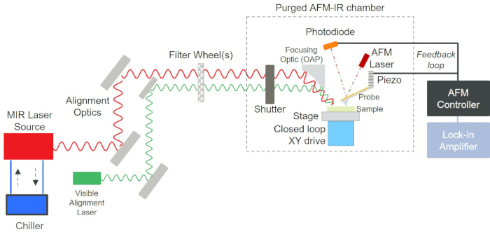
Figure 3. Generalized schematic block diagram of a typical AFM–IR system. The diagram illustrates the infrared laser source, visible alignment laser, alignment optics, shutter, focusing optics, AFM probe assembly, photodiode detector, lock-in amplifier, AFM controller, sample stage, and environmental purge enclosure used during AFM–IR measurements. Abbreviations: AFM = atomic force microscope; MIR = mid-infrared; OAP = off-axis parabolic reflector. Please click here to view a larger version of this figure.
- Initiate purge-gas flow through the IR beam path and instrument enclosure at approximately 4 L/min. Use ultrahigh-purity (99.999%) N₂ as the purge gas when available, or compressed dry air when N₂ is unavailable8.
NOTE: Purging displaces atmospheric H2O and CO2 that absorb in the IR spectral region. Maintaining a low purge-gas flow rate during instrument setup reduces the purge time required immediately prior to data acquisition (see Step 1.25). - Consult the laser user manual to confirm the required laser-chiller coolant composition.
NOTE: The broadband optical parametric oscillator (OPO) source used in this study (APE Carmina) operates at 22°C using a 3:1 mixture of distilled water and Innovatek Protect IP concentrate. The MIRcat QCL quantum cascade laser operates at 21°C using 10% isopropyl alcohol in distilled water. Both chillers have a capacity of approximately 450 mL, a maximum flow rate of 4 L/min, and a nominal temperature stability of ±0.1°C. During AFM–IR measurements, both chillers operate at 20% pump drive and typically achieve temperature stability of ±0.01°C to ±0.03°C over 15 min to 1 h. - Verify that the appropriate coolant is circulating before powering the IR source.
NOTE: Lasers often require chillers to remove excess heat and maintain a stable operating temperature to ensure stable output power, wavelength, mode quality, and beam pointing. Chiller coolants help preserve component lifetimes by preventing corrosion and/or algal growth. - Power on the laser power supply, AFM controller, IR source(s), and associated instrumentation (e.g., laser chiller(s) and lock-in amplifier(s)).
- Allow all equipment to warm up according to the manufacturer’s recommendations (typically 15–60 min).
- Start Analysis Studio v3.17 AFM control software.
- Open the Hardware Configuration menu from the Setup dropdown menu.
- Select the instrument configuration appropriate for the AFM–IR system from the Active Config dropdown menu to load the correct system configuration file.
- Click the Initialize icon and confirm communication between the IR source(s), AFM controller, and lock-in amplifier(s) by verifying that no startup error messages are displayed.
NOTE: An incorrect configuration may require assistance from the instrument vendor. - Select the experimental configuration appropriate for the planned measurement (e.g., Tapping AFM–IR Mode) from the dropdown menu in the AFM Scan window.
- Select the New icon in the Analysis Studio toolbar to create a new project where all data will be saved. Use the Save As option in the File menu to specify the desired project filename.
- Select an AFM–IR probe compatible with the sample, illumination geometry, and imaging mode. Use a gold-coated TnIR-D-10 high-stiffness tapping-mode AFM–IR probe for most heterodyne-detected tapping-mode AFM–IR measurements on the Bruker nanoIR3 AFM–IR system.
NOTE: The high-stiffness tapping-mode AFM–IR probe has a nominal tip radius of 20 nm, spring constant of 42 N/m, and resonance frequency of 320 kHz. A gold-coated TnIR-A-10 low-stiffness tapping-mode AFM–IR probe may be used for softer samples when lower cantilever stiffness is desired. The low-stiffness tapping-mode AFM–IR probe has a nominal tip radius of 20 nm, spring constant of 3 N/m, and resonance frequency of 75 kHz. See Discussion for more details regarding appropriate probe choice and relevant considerations. - Mount the selected probe onto the AFM head (Figure 4A, 4B).
NOTE: AFM–IR probes used for top-down illumination typically contain a thin Au or Pt coating on the cantilever and substrate. The coating minimizes probe IR absorption, produces a flatter spectral response, and enhances the local electric field at the probe apex through the lightning-rod effect, thereby increasing localization and wavelength-independent amplification of the photothermal signal8,15,16,77,78,79,80,81. - Mount the sample on a magnetic specimen disc compatible with the AFM–IR system sample chuck, securing the sample using double-sided carbon tape, silver paste, fingernail polish, superglue, or epoxy.
NOTE: Use a conductive adhesive such as carbon tape or silver paste if electrical AFM modes or subsequent electron microscopy characterization will be performed. - Select the Load icon in the AFM Probe window to open the Load Tip Wizard window.
- Verify that the probe and sample region of interest are visible within the optical field of view (Figure 4C, 4D).
NOTE: Samples up to approximately 25 mm in diameter can be accommodated on the sample chuck; however, only the central 6 mm × 8 mm region is accessible for AFM–IR measurements. The region of interest will be dependent on what the user desires to interrogate with AFM–IR, but use visual markers in combination with sample schematics to distinguish and identify a site. - Adjust the optical focus using the up/down arrows in the Focus on Probe window until the cantilever edges nearest the probe apex are clearly resolved, then click Next.
- Position the crosshair directly over the probe tip at the distal end of the cantilever in the Center Crosshairs window, which will center the probe tip in the optical field of view, then click Next.
- Adjust the optical focus using the up/down arrows in the Focus on Sample window until sample surface features are clearly resolved.
- Use the Sample XY Navigation stage control arrows and the optical microscope view to navigate the sample until the area of interest is positioned beneath the probe tip, then click Next.
- Set a Standoff distance of at least 100 µm and select Approach Only.
NOTE: After clicking Approach Only, the tip will approach to within the Standoff distance of the sample surface and the Load Tip Wizard window will close automatically. - Use the AFM laser-alignment control knobs to position the AFM laser on the back of the cantilever directly above the probe tip and maximize the laser-sum voltage (Figure 4C).
- Center the laser laterally on the cantilever.
- Position the laser near the cantilever apex above the probe tip.
- Adjust the laser position until the maximum laser-sum voltage is achieved.
NOTE: Verify that the laser-sum voltage exceeds 5 V when using a high-stiffness tapping-mode AFM–IR probe. If not, the probe may be damaged or not properly mounted.
- Adjust the photodetector-alignment control knobs to center the reflected laser beam on the position-sensitive photodiode.
- Adjust the alignment until the deflection signal is within ±0.1 V of zero.
- Verify that the Deflection readout displays a green indicator centered in the readout field (Figure 4E).
- Close the instrument enclosure.
- Increase the purge-gas flow rate to approximately 7 L/min and continue purging until the enclosure humidity decreases below 8%.
- Reduce the purge-gas flow rate to approximately 4 L/min to maintain the reduced humidity level throughout subsequent measurements.
NOTE: Reducing the purge-gas flow rate minimizes turbulence that may introduce AFM imaging noise. Samples exhibiting stronger IR absorbance are generally less sensitive to residual humidity. Under some circumstances, humidity levels as high as approximately 10% may be acceptable, allowing shorter purge times and lower gas consumption while minimizing turbulence.
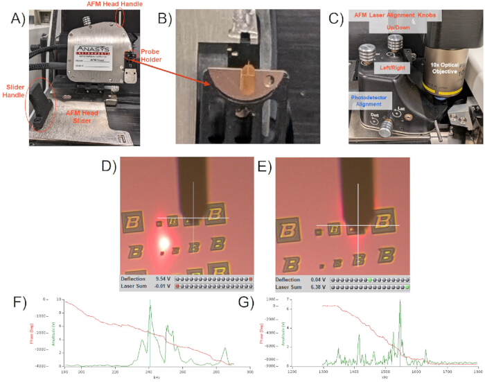
Figure 4. Instrument setup, probe alignment, and cantilever tuning for a nanoIR3-s AFM–IR system running Analysis Studio v3.17. (A) AFM head assembly showing the AFM head handle, slider handle, and head-positioning components. (B) Probe holder containing a pre-mounted TnIR-D-10 AFM–IR probe. (C) Alignment controls used to position the AFM deflection laser on the cantilever and center the reflected beam on the position-sensitive photodiode. (D) Optical image of the sample and AFM probe before laser alignment, showing a low laser-sum signal. (E) Optical image after laser alignment, showing a laser-sum signal greater than 5 V and near-zero cantilever deflection. (F) Representative tuning curve of the TnIR-D-10 probe’s first resonance frequency (f₁) at approximately 240 kHz used for topography acquisition (Drive Mode). (G) Representative tuning curve of the higher-frequency resonance (f₂) at approximately 1550 kHz used for photothermal detection (Detection Mode). Please click here to view a larger version of this figure.
2. Probe Tuning
- Perform a pair of cantilever tunes to determine the probe resonance frequencies to use for Drive and Detection Mode (Figure 4F, 4G).
NOTE: Following the procedure below will ensure that the cantilever tune produces well-separated resonance peaks for both the topography (Drive Mode) and IR detection (Detection Mode) resonances.- Confirm Tapping AFM–IR mode is selected from the dropdown menu in the AFM Scan window.
- Click the tuning fork icon to open the Cantilever Tune window.
- Perform the Drive Mode cantilever tune.
- In the Drive Mode tune panel, set a frequency sweep range of approximately 100 kHz around the nominal resonance frequency of the probe (Figure 4F), then click the green Start arrow.
NOTE: The nominal resonance frequency is typically listed on the box the AFM probe comes in. - Identify the resonance peak to use for tapping-mode topography imaging. Select a prominent isolated Gaussian-shaped peak without a significant shoulder. The highest amplitude peak in the frequency sweep range that fits these criteria is generally best.
- Reduce the sweep range to approximately 10 kHz and refine the selected resonance frequency until the peak frequency is clearly resolved.
NOTE: Select a Drive Mode frequency slightly below the resonance peak such that it reduces the free-space oscillation amplitude by approximately 5% relative to the peak amplitude (Figure 4F). This offset helps compensate for attractive van der Waals interactions during approach and promotes operation within the repulsive interaction regime during tapping-mode imaging. - Adjust the Drive Mode Strength until a peak amplitude of approximately 9 V is achieved.
NOTE: The Drive Mode Strength is typically 0.2%–5%.
- In the Drive Mode tune panel, set a frequency sweep range of approximately 100 kHz around the nominal resonance frequency of the probe (Figure 4F), then click the green Start arrow.
- Perform the Detection Mode cantilever tune.
- In the Detection Mode tune panel, set the center frequency to approximately six times the Drive Mode frequency.
- Set the Detection Mode sweep range to approximately 500 kHz (Figure 4G), then click the green Start arrow.
- Select the most prominent isolated Gaussian-shaped resonance peak in the Detection Mode frequency spectrum without a significant shoulder. The highest amplitude peak in the frequency sweep range that fits these criteria is generally best.
- Reduce the sweep range to approximately 10–20 kHz and refine the selected Detection Mode frequency until the resonance peak is clearly resolved.
- Adjust the Detection Mode Strength until a peak amplitude of approximately 9 V is achieved.
NOTE: The Detection Mode Strength is typically 5%–50%. - Set the Detection Mode frequency to the maximum amplitude of the selected resonance.
NOTE: The selection of the Drive and Detection Mode resonances for heterodyne-detected tapping-mode AFM–IR may significantly affect the measured IR response during imaging and spectral acquisition. The optimal choice depends on both the AFM probe cantilever resonance peaks and the capabilities or limitations of the instrument hardware, including maximum dither-piezo frequency and controller bandwidth. In this protocol and in Figure 4F, 4G, f1 is used for topography acquisition (Drive Mode), and f2 is used for IR detection (Detection Mode). Refer to the Discussion for considerations in selecting Drive and Detection resonances, including cases in which switching the order of the Drive and Detection Mode frequencies may be preferable.
- Click the green Accept Cantilever Tune check mark icon to save the Drive and Detection Mode settings.
3. AFM (Topography) Imaging
- Click the green Engage icon in the AFM Probe window to engage the probe on the sample surface.
CAUTION: Monitor the live video feed in the Microscope window throughout the engage process. Withdraw the probe immediately if the laser spot shifts off the probe cantilever, if the cantilever bends excessively (photodetector deflection ≥ ~5 V), or if the cantilever snaps during engagement. - Verify successful probe engagement by confirming that the Laser Sum signal remains near its free-space value and that fluctuations in the Z Position monitor remain below ±0.2 µm (i.e., the Z Position status bar indicator light fluctuates by plus or minus one position or less).
- Disable IR imaging after successful probe engagement by deselecting the IR Imaging Enabled checkbox in the NanoIR window.
- Begin AFM scanning by selecting the Scan icon in the AFM Scan window.
- Ensure the Feedback is On (radio button).
- Set the tapping-mode amplitude Setpoint to less than 8 V.
NOTE: Operating with an amplitude setpoint of approximately 70%–90% of the free-space amplitude (approximately 6–8 V for a 9 V Drive Mode free-space amplitude as in Step 2.2.4) generally provides good topographic tracking. Lower setpoints may improve tracking of high-aspect-ratio features but increase the risk of damaging the probe and/or sample. - Optimize the feedback gains by setting the gains to achieve the best trace and retrace overlap – increase the gains until feedback noise becomes apparent in the topography image and/or error channel, then reduce the gains until the increased noise disappears.
NOTE: Typical gain values are 3–5 for the I (Integral) Gain and 5–7 for the P (Proportional) Gain. - Select a scan size (Width and Height) appropriate for the feature(s) of interest.
NOTE: Scan sizes of 5–20 µm were used in this work. The maximum XY scan size of the AFM–IR system is 50 µm. Select a scan size that fully encompasses the feature(s) of interest while providing sufficient pixel resolution to resolve those features within the limits imposed by tip-radius convolution. - Select a scan rate that provides acceptable trace-retrace overlap while maintaining practical acquisition times.
NOTE: The greater the separation between the trace and retrace lines, the less the probe is accurately tracking the topography of the sample. In general, this separation increases with faster scan rates. However, the slower the probe scans, the longer it takes to acquire data. Scan rates of approximately 0.5–2 Hz typically provide a suitable balance between acquisition speed and noise. For typical scan sizes of 5–20 µm, this corresponds to probe velocities of approximately 10–20 µm/s. The probe velocity is calculated by multiplying twice the scan size (to account for trace and retrace motion) by the scan rate. Exceptions to these ranges can exist, for instance, a very rough sample (e.g., Rq > 30 nm) may need to be scanned at a probe velocity of <10 µm/s, while an atomically flat sample (e.g., Rq < 1 nm) could be tracked well at a probe velocity of >20 µm/s. - Select the lateral (X and Y) pixel resolution.
NOTE: The maximum image size supported by the AFM–IR system is 1024 × 1024 pixels. Pixel resolution is the scan size divided by the number of pixels per line. However, physical resolution is limited by the probe tip radius. For example, a high-stiffness tapping-mode AFM–IR probe has a nominal tip radius of 20 nm; therefore, selecting a lateral pixel spacing substantially less than ~20 nm may result in oversampling and worse S:N with little or no improvement in physical resolution. - Apply X and Y piezo Offsets as needed to center the region of interest within the scan area.
- Continue scanning while iteratively adjusting the amplitude setpoint and feedback gains to optimize image quality by verifying that the trace and retrace overlap and the error signal is minimized (i.e., the feedback gains have been increased until just before an increase in noise becomes apparent, as described in Step 3.7) for the selected scan size, scan rate, and pixel resolution.
- After imaging parameters have been optimized, continue scanning the full area to capture an image of the area of interest for IR analysis.
NOTE: As shown in the Representative Results, the area to be scanned is dependent on the specific sample needs (e.g., point-selective IR spectral analysis of a contaminant, IR mapping of the spatial distribution of a specific chemical functional group, etc.). - Select the Stop icon in the AFM Scan window to stop scanning after the topography map has been completed and site(s) of interest are confirmed.
NOTE: If desired (e.g., if only IR point spectra will be subsequently collected rather than IR maps, but correlation of IR spectra with topographical features is desired), save the AFM topography image by selecting Capture: Last Frame from the Microscope window toolbar.
4. IR Laser Alignment and Optimization
- Identify a likely IR-active feature of interest in the AFM topography image.
NOTE: Identification of an IR-active feature of interest may be an iterative process, depending on extent of a priori knowledge of sample composition as well as correspondence (or lack thereof) between topographical features and identifiable IR-active features. Accordingly, it can be useful to fabricate an IR-alignment sample such as the polyethylene terephthalate (PET) blanket film on a highly reflective substrate shown in Figure 5. - Move the probe to the selected feature using the point-and-click navigation function in the Microscope window’s live video feed.
- Click the Align icon in the NanoIR window to open the Load Tip Wizard window. This will enable the visible alignment laser that is colinear with the IR laser path (Figure 5A, 5B).
- Adjust the IR focus using the Adjust IR Focus up and down arrows in the Center Align Laser window to identify the focal position that produces the smallest, most circular visible laser spot (Figure 5B).
NOTE: A highly reflective sample will make it easier to see the visible laser beam if it is not hitting the cantilever. - Center the visible alignment laser on the back of the cantilever directly above the probe tip using the Align Laser Navigation arrows.
- Click Finish to close the Load Tip Wizard window.
NOTE: Steps 4.3–4.6 provide coarse alignment only. Final optimization of beam alignment and focus is performed using the IR beam in subsequent steps to ensure a measurable photothermal response from the sample (Figure 5C, 5D). - Select an IR wavenumber corresponding to a known IR-active vibrational mode of the feature of interest.
NOTE: Prior knowledge of the expected chemical composition and corresponding IR absorption bands may simplify optimization. For example, carbonyl (C=O) groups commonly exhibit strong IR absorbance near 1720–1730 cm−1. - Verify that all required laser-safety procedures are in place before enabling the IR source.
CAUTION: IR radiation is invisible and may cause serious eye injury. Follow all applicable laser-safety requirements before enabling the IR source, including signage, safety interlocks, shutters, enclosure controls, and laser-safety eyewear when required. The broadband OPO source is a Class 4 laser system, and the QCL source is a Class 3B laser system. As installed, the AFM–IR system is Class 2 because beam tubes contain the laser beams and safety interlocks engage shutters when the AFM–IR enclosure is open. Because the shutters are designed to fail closed upon loss of power, laser-safety eyewear is not required during routine operation unless interlocks are defeated or shutters are forced open during maintenance or beam realignment. When eyewear is required, use IR laser-safety glasses that protect across the full IR laser range, such as Schott-glass IR laser-safety glasses. - Select the desired incident IR Power from the dropdown menu of available attenuation levels in the NanoIR window based on the available neutral density filter wheel combinations.
NOTE: Excessive IR power may thermally damage sensitive materials. For polymer-based samples on the AFM–IR system, maintain IR power below approximately 20%. - Set the laser Duty Cycle in the NanoIR window.
NOTE: For the broadband OPO source, use a duty cycle of 50%. For the QCL, use a duty cycle below 10%, typically 2%–4%. For QCL operation, duty cycle and neutral-density filtering jointly determine incident IR power, with power scaling linearly with duty cycle. The software automatically adjusts the QCL pulse duration from 40 ns to 500 ns in 20 ns increments to match the selected duty cycle and pulse repetition rate. - Click the Optimize icon in the NanoIR window to open the IR Optimize window.
- Adjust the slider bar at the top of the IR Optimize window to select an area larger than 200 µm × 200 µm and click Scan to raster the IR beam.
- If necessary, adjust the IR focus to compensate for differences between the visible alignment and IR beams. To do this, click on Tools and select Focus Capture. Select a Number of Focus Captures (e.g., 5) as well as focus Start and End points, then click Focus Capture to simultaneously optimize beam alignment and focus.
NOTE: A properly aligned beam should produce a roughly Gaussian response profile. Figure 5C shows a beam-optimization map obtained when the sample is IR-inactive at the selected wavenumber and/or when the IR alignment and focus are poorly optimized. Figure 5D shows a representative optimized beam with a spot size of approximately 40–50 µm and a photothermal response of approximately 3 mV above background. A beam spot size of < 100 µm with a photothermal response of > 0.5 mV above background is generally acceptable; however, this will be dependent on the exact input beam size, mode quality, divergence, and wavelength, as well as the beam pathway design (e.g., focusing optics, neutral density filters, etc.). The magnitude of the photothermal response is also heavily dependent on the IR absorption strength of the sample itself, which depends on the magnitude of the change in the bond’s dipole moment during vibration and the number of those bonds present in the probe’s near-field response area. - Repeat beam optimization at additional wavenumbers when spectra or chemical maps will be acquired across a broad spectral range.
NOTE: Beam alignment and focus may vary as a function of wavelength; therefore, optimize beam alignment and focus at multiple wavenumbers when spectra or chemical maps will be acquired across a broad spectral range8. - Click OK to close the IR Optimize window and save settings.
- Click the Pulse Tune icon in the NanoIR window to open the Laser Pulse Tune window.
- Set a Tune Range of approximately 100–200 kHz centered on the nominal difference-frequency Pulse Rate identified during probe tuning.
NOTE: The nominal pulse repetition rate is equal to |f₂ − f₁|, where f₁ and f₂ are the selected Drive and Detection resonance frequencies. - Sweep the laser pulse repetition rate over the selected Tune Range about the Pulse Rate by clicking Acquire.
- Verify that a prominent isolated Gaussian-shaped resonance peak without a significant shoulder is observed, similar to Steps 2.2.2 and 2.3.3 in the Probe Tuning when selecting the Drive and Detection Mode resonances.
NOTE: Increase the sweep range to as much as 1,000 kHz if a clear resonance peak meeting the above criteria is not observed. - Select the identified resonance peak. The highest amplitude peak in the selected laser pulse repetition rate (frequency) range that fits the selection criteria is generally best and should produce the strongest heterodyne-amplified IR absorption response.
- Reduce the Tune Range to be swept to ≤50 kHz.
- Refine the selected pulse repetition rate by locating the maximum of the resonance peak.
- Enable the PLL under Auto-Tune.
NOTE: The PLL maintains the laser pulse repetition rate at the difference frequency between the selected cantilever eigenmodes, compensating for resonance-frequency drift during measurement15. - Set the PLL bandwidth to ≤ ±30 kHz around the selected resonance by setting corresponding Minimum and Maximum allowable frequencies.
- Set the PLL threshold slightly above the observed noise level in the pulse-tune (~1.1 times the noise).
- Click OK to close the Laser Pulse Tune window and save the settings.
NOTE: Reconfirm laser alignment if the optimized pulse repetition rate differs substantially from the value obtained during the initial probe tune. - Select Tools > IR Background Calibration from the main menu.
- Click New to acquire a background spectrum, I₀(ṽ).
- Confirm the Pulse Rate and Duty Cycle are equal to the values established during IR optimization.
- Set the spectral Resolution (cm−1/pt) equal to the value planned for sample acquisition.
NOTE: The maximum achievable spectral resolution is IR source dependent (<1 cm−1 for the MIRcat QCL and ~20 cm−1 FWHM for the APE Carmina operating in narrowband mode). Additional considerations in selecting the spectral resolution are expected vibrational linewidths and spacing of spectral features (if known), reasonable acquisition time (which scales linearly with resolution), and desired S:N (which decreases with increased spectral resolution). Commercial FTIR spectrometers for analyzing solid samples typically offer user-selectable resolutions of 1, 2, 4, 8, or 16 cm−1, with 4 cm−1 resolution a commonly used setting. - Select Start and End Wavenumbers that encompass the entire spectral range intended for sample measurements.
- Set Power to 100%.
- Set Backgrounds to Average to 5 acquisitions.
- Click Acquire to acquire the averaged background spectrum.
NOTE: A quality background spectrum should mirror the shape of the manufacturer’s IR laser power output versus wavelength spectrum. Refer to the data sheet/manual of the laser(s). Additional absorption features can occur in the background spectrum if the AFM−IR chamber is not adequately purged (e.g., water is typically observed as a series of absorption peaks between approximately 1250 and 2000 cm−1, with maxima at ~1550 and ~1700 cm−1, plus a broad ~300 cm−1 wide FWHM absorption centered at 3750 cm−1, while CO2 is typically seen as a broad absorption at ~2325 cm−1). Consult the NIST Chemistry WebBook (https://webbook.nist.gov/chemistry/) for representative vapor phase IR spectra of H2O and CO282. - Click Save to save the background spectrum and automatically close the Collect Background window.
NOTE: During IR Spectral Acquisition, the software will automatically divide the measured photothermal response by the IR Background Calibration file to correct for the variation in laser output power as a function of wavelength/wavenumber (i.e., the laser output spectrum).
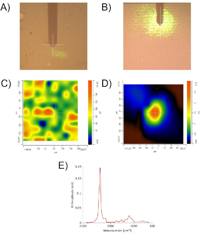
Figure 5. IR laser alignment and optimization workflow. (A) Optical image of an AFM probe with the visible alignment laser out of focus and not centered on the cantilever. (B) Visible alignment laser centered on the cantilever directly above the probe tip after optimization of focus and positioning. (C) Example raster scan of a 200 µm × 200 µm area with a Carmina OPO tuned to 1730 cm⁻1 and filtered to 11.39% power, acquired under non-optimized beam-alignment and focusing conditions. The sample was effectively IR-inactive at the selected wavenumber and/or the IR focus was poorly aligned with the tip–sample interface; therefore, no localized high-intensity photothermal response was detected. (D) Optimized raster scan of the beam centered on the same 200 µm × 200 µm area around the probe tip, showing a centered and approximately Gaussian laser profile with a spot size of 40–50 µm and a strong photothermal response with a maximum intensity of approximately 3 mV. (E) Representative raw heterodyne-detected tapping-mode AFM–IR spectrum acquired at 2 cm⁻1/point resolution from a polyethylene terephthalate (PET) alignment sample following optimization of IR beam alignment to the probe tip at 1730 cm⁻1. The y-axis corresponds to the photothermal AFM–IR response measured in millivolts of signal on the beam-bounce photodiode at the Detection Mode frequency. Please click here to view a larger version of this figure.
5. IR Spectral Acquisition
- Identify the feature of interest in the previously acquired AFM topography image, then position the AFM probe over the selected feature in the Imaging View using the Microscope window point-and-click navigation function.
- Define the desired spectral acquisition range (Start and End in cm−1) in the NanoIR window based on available laser coverage and expected vibrational modes of interest (if known).
NOTE: The APE Carmina used here covers 5–15 µm (~670–2000 cm−1), while the MIRcat QCL has 4 chips covering 755–1005, 955–1425, 1425–1835, and 2635–3000 cm−1. For the patterned silicon wafer and polymer samples shown here, the approximate spectral range of interest is 1000–1800 cm−1. - Set the Spectra Resolution (cm−1/point) in the NanoIR window to match the value used during IR Background Calibration.
- Select the desired IR laser Power from the dropdown menu in the NanoIR window.
NOTE: See Note on Step 4.9 and Discussion for details regarding incident IR power considerations. - Specify the number of spectra to acquire in the NanoIR window.
NOTE: Although the default is one spectrum, acquiring multiple spectra enables evaluating spectrum-to-spectrum variability and allows manual co-averaging of spectra in post-processing to improve S:N. - If spectral averaging is desired to improve S:N, ensure the Co-average Spectra checkbox is selected and specify the desired number of spectra Co-averages from the dropdown menu in the NanoIR window.
NOTE: S:N will improve as the square root of the number of co-averages, while the time required for acquisition will increase linearly, so there is a point of diminishing returns to increasing the co-averages. - Click Acquire in the NanoIR window to start acquisition of an IR spectrum.
- If desired, export and save the acquired spectrum by selecting Export from the File dropdown menu in Analysis Studio.
NOTE: Available file formats for exporting spectra include CSV, TSV, and Image (TIFF, GIF, BMP, PNG, or JPEG). In addition to the IR spectrum XY data (i.e., IR amplitude as a function of IR wavenumber), CSV or TSV files will include the user-selected IR power percentage, beam shape factor, and PLL frequency, as well as the IR Background Calibration data used to scale the raw photothermal response and correct for the laser output power spectrum (see Step 4.35). Images will not contain any metadata. - Repeat the acquisition at additional locations as needed.
NOTE: See Results and Discussion for examples of parameter selection and interpretation of AFM–IR spectra.
6. IR (Vibrational Mode) Mapping
- Set the IR wavenumber in the NanoIR window to the amplitude maximum of the vibrational mode of interest based on the IR spectrum acquired in Step 5.
NOTE: Pick a vibrational mode (spectral peak) that exhibits high amplitude and provides the greatest material contrast (i.e., a peak that is only found in or significantly stronger in one material component), as shown in the Representative Results (e.g., the 1730 cm−1 carbonyl stretch of PMMA in Figures 6 and 9, the 1120 cm−1 Si–O stretch of SiO2 in Figure 7, or the 1600 cm−1 aromatic stretching mode of the photoresist residue in Figure 8). IR correlation charts, published or locally acquired IR spectra, or publicly available spectral databases such as the NIST Chemistry WebBook can be consulted for peak assignments82. - Select the IR Imaging Enabled checkbox in the NanoIR window.
- Begin AFM scanning by clicking the Scan icon in the AFM Scan window. This will start simultaneous acquisition of the AFM topography image and corresponding IR amplitude map.
NOTE: Typically, the same AFM Scan parameters can be used for IR Mapping as were used previously to acquire the AFM topography image in Step 3. See Representative Results and Discussion for examples of parameter selection and interpretation of AFM–IR chemical maps. - Select Capture: End of Frame from the Microscope window toolbar to save the AFM topography image and IR mapping data.
NOTE: The saved AFM topography and IR mapping data can be exported as either an Image (TIFF, GIF, BMP, PNG, or JPEG) or Gwyddion (*.gsf) AFM data file for subsequent offline post-processing and data analysis if desired by selecting Export from the File dropdown menu in Analysis Studio. While metadata regarding data acquisition parameters is available in the Analysis Studio Project file, the exported image or AFM data files will not include it. In contrast with AFM topography data, IR maps are typically displayed as acquired, with no post-processing performed or necessary (e.g., plane-fitting or flattening), similar to other non-topography SPM modes such as CAFM/TUNA, KPFM, or MFM.
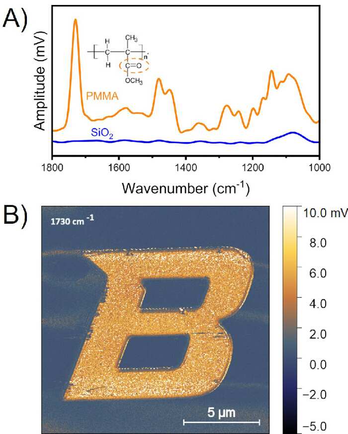
Figure 6. AFM–IR spectroscopy and chemical mapping of patterned poly(methyl methacrylate) (PMMA). PMMA was patterned on a thermally oxidized Si/SiO₂ substrate using a Teneo Nabity NPGS electron-beam lithography (EBL) system. Measurements were performed using resonance-enhanced contact-mode AFM–IR with a CnIR-B-10 probe and a MIRcat QCL filtered to 14.75% IR power and tuned to a laser pulse repetition rate of approximately 782 kHz corresponding to a contact resonance of the probe maintained at a deflection setpoint of 2 V (approximately 4 nN load). (A) AFM–IR spectra acquired from PMMA (orange) and SiO₂ (blue) regions of the sample. Spectra represent the average of five sequential acquisitions collected at the same location with a spectral resolution of 2 cm-1/point. Spectra were smoothed in Origin v10.0.5.157 using a third-order Savitzky–Golay filter with a rolling 10-point window, and the PMMA spectrum was vertically offset for clarity. The inset shows the PMMA molecular structure, with the carbonyl (C=O) functional group highlighted. (B) AFM–IR chemical map acquired at 1730 cm-1, corresponding to the PMMA carbonyl absorption band. The map covers a 15 µm × 15 µm region acquired at a scan rate of 0.5 Hz and 30 nm pixel resolution (500 × 500 pixels). A phase-locked loop (PLL) was enabled throughout image acquisition to track changes in the contact-resonance frequency. Please click here to view a larger version of this figure.
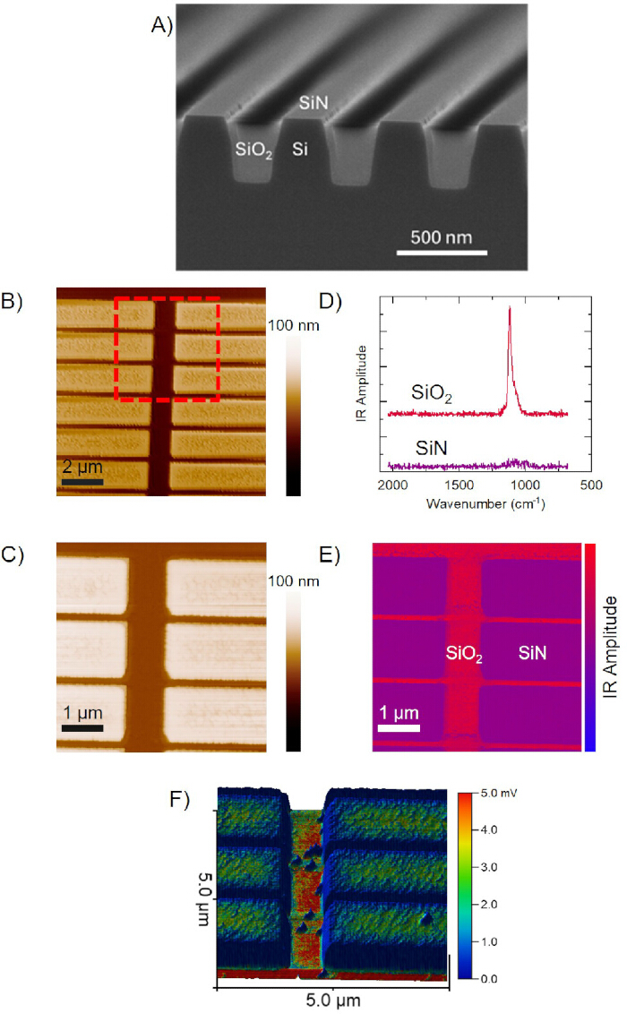
Figure 7. AFM–IR characterization of area-selective deposition (ASD) of polypyrrole (PPy) on patterned silicon structures. Measurements were performed using heterodyne-detected tapping-mode AFM–IR and a TnIR-D-10 probe. A Carmina OPO was filtered to 4.15% IR power and tuned to a laser pulse repetition rate of approximately 258 kHz, corresponding to the difference between the Drive and Detection Mode frequencies for heterodyne amplification of the photothermal IR-response signal, with the PLL bandwidth set to ±25 kHz. (A) Cross-sectional scanning electron microscopy (SEM) image of the patterned wafer showing SiN-covered silicon ridges adjacent to SiO₂ trenches. (B, C) 256 × 256 pixel AFM topography images of representative patterned regions displaying (B) a 10 µm × 10 µm area at approximately 40 nm pixel resolution and (C) a 5 µm × 5 µm area at approximately 20 nm pixel resolution. (D) Raw AFM–IR spectra acquired from SiO₂ and SiN regions, with a spectral resolution of 2 cm-1/point, showing the characteristic Si–O stretching mode at approximately 1120 cm-1. (E) AFM–IR chemical map acquired at 1120 cm-1. Increased signal intensity corresponds to stronger Si–O absorption. (F) Three-dimensional rendering of the AFM–IR response at 1120 cm-1 overlaid on sample topography following PPy deposition. Localized deposition is observed within the SiO₂ trenches. Pixel resolution of the 5 µm × 5 µm IR maps shown in (E) and (F) is approximately 20 nm (256 × 256 pixels). Maps were acquired at a scan rate of 0.5 Hz. Underlying data and figure adapted with permission under a CC BY 4.0 license from Figure 6 in Thelven et al.44. Please click here to view a larger version of this figure.
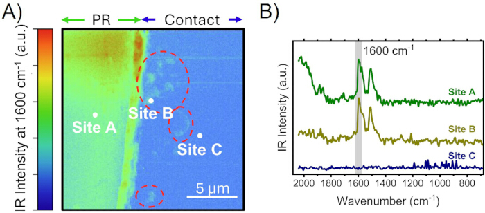
Figure 8. AFM–IR analysis of a photoresist-removal process. Measurements were performed using heterodyne-detected tapping-mode AFM–IR and a TnIR-D-10 probe. A Carmina OPO was filtered to 4.15% IR power and tuned to a laser pulse repetition rate of approximately 266 kHz, corresponding to the difference between the Drive and Detection Mode frequencies for heterodyne amplification of the photothermal IR-response signal, with the PLL bandwidth set to ±25 kHz. (A) AFM–IR chemical map of a 20 µm × 20 µm area acquired at a scan rate of 0.3 Hz with 50 nm pixel resolution (400 × 400 pixels) and the IR laser tuned to 1600 cm-1, corresponding to aromatic-ring vibrations characteristic of the photoresist. Regions of suspected residual contamination are highlighted with dashed outlines. Horizontal streaks caused by poor probe tracking of abrupt features were removed using the scar-correction function in Gwyddion v2.69. (B) AFM–IR spectra acquired at 1 cm-1/point resolution from the locations indicated in (A). Site A corresponds to photoresist, Site B corresponds to a contaminated contact region, and Site C corresponds to a nominally clean Ga₂O₃ surface. The shaded region indicates the spectral range used to generate the chemical map based on the sample photothermal response at 1600 cm-1. Spectra were smoothed using an FFT post-processing filter in Gwyddion v2.69. Underlying data and figure adapted with permission under a CC BY 4.0 license from Figure 6 in Pieczulewski et al.45. Please click here to view a larger version of this figure.
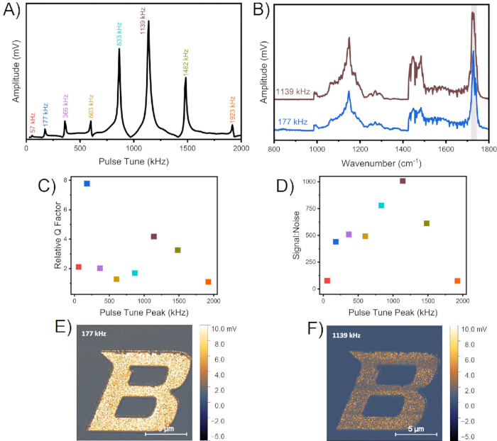
Figure 9. Influence of contact-resonance selection on resonance-enhanced contact-mode AFM–IR performance. Measurements were performed on a single EBL-patterned PMMA-on-Si/SiO₂ sample using resonance-enhanced contact-mode AFM–IR and a CnIR-B-10 probe maintained at a deflection setpoint of 2 V (approximately 4 nN load), with a MIRcat QCL filtered to 17.85% IR power. The QCL pulse repetition rate was varied to correspond to different observed contact-resonance frequencies, with the PLL bandwidth set to ±30 kHz. (A) Contact-resonance sweep acquired from PMMA on a Si/SiO₂ substrate with the laser tuned to the PMMA carbonyl absorption band at 1730 cm-1. (B) AFM–IR spectra acquired using laser pulse repetition rates of 177 kHz and 1139 kHz. Spectra represent the average of five sequential acquisitions collected at the same location, normalized to the height of the 1730 cm-1 carbonyl peak, and vertically offset for clarity. (C) Relative Q factors calculated from the measured resonance peaks. (D) Relative signal-to-noise (S:N) ratios calculated as the ratio of the PMMA carbonyl peak intensity to the root-mean-square baseline noise. (E, F) Raw AFM–IR chemical maps acquired at a scan rate of 0.8 Hz from a single 15 µm x 15 µm scan at 1730 cm-1 with 30 nm pixel resolution (500 × 500 pixels) using laser pulse repetition rates of (e) 177 kHz and (f) 1139 kHz. For ease of comparison, the raw data maps in (E) and (F) are displayed using the same color scale. Please click here to view a larger version of this figure.
Access restricted. Please log in or start a trial to view this content.
Results
In the semiconductor field, a thermoplastic such as poly(methyl methacrylate) (PMMA) can be used as an insulator and blended with active semiconducting polymers to tune device charge mobility77,78. PMMA also has utility as a positive resist for electron-beam or ultraviolet lithography79. In either application, AFM–IR can be used to confirm polymer distribution after processing. In Figure 6A, 6B
Access restricted. Please log in or start a trial to view this content.
Discussion
Selecting the appropriate probe for the AFM–IR geometry (i.e., top-down versus bottom-up illumination) and operating mode (e.g., tapping-mode versus contact-mode AFM–IR) is an important consideration for obtaining optimal, artifact-free data. General probe characteristics to consider include the nominal spring constant and resonance frequency, which typically scale together. Higher resonance frequencies, and therefore larger spring constants (i.e., stiffer cantilevers), are generally preferred for tapping-mod...
Access restricted. Please log in or start a trial to view this content.
Disclosures
The authors have nothing to disclose.
Acknowledgements
The Bruker Anasys nanoIR3-s AFM–IR system used in this work was acquired with support from the M. J. Murdock Charitable Trust (Award No. 202014907). The system is located in the Boise State University Surface Science Laboratory (SSL), which is part of the FaCT Core Facility, RRID: SCR 024733, and receives support from the National Institutes of Health (NIH) under the Institutional Development Awards (IDeA) Program of the National Institute of General Medical Sciences via Grant Nos. P20GM148321 and P20GM103408, the former of which also partially supports co-authors C.M.E. and P.H.D. N.O. is supported by the Superior Energy-efficient Materials and Devices (SUPREME) Center, a Semiconductor Research Corporation (SRC) program sponsored by the Defense Advanced Research Projects Agency (DARPA). This material is based on research sponsored by the Air Force Research Laboratory (AFRL) under Agreement Number FA8650-20-2-5506 in support of AFRL. The U.S. Government is authorized to reproduce and distribute reprints for Governmental Purposes notwithstanding any copyright notation thereon. The views and conclusions contained herein are those of the authors and should not be interpreted as necessarily representing the official policies or endorsements, either expressed or implied, of AFRL, NIH, or the U.S. Government.
Access restricted. Please log in or start a trial to view this content.
Materials
| Name | Company | Catalog Number | Comments |
|---|---|---|---|
| AFM control software | Bruker | Analysis Studio v3.17 | Instrument control, AFM imaging, AFM–IR acquisition, and data analysis. |
| AFM image processing and analysis software | Gwyddion | V2.69 | AFM data processing and analysis. |
| AFM–IR probe(s), contact mode | Bruker | PR-EX-CNIR-B-10 | Resonance-enhanced contact-mode AFM–IR probe; nominal spring constant (k) = 0.2 N/m, resonance frequency (f0) = 13 kHz, tip radius (r) = 20 nm, Au-coated cantilever and tip. |
| AFM–IR probe(s), tapping mode | Bruker | PR-EX-TNIR-D-10 | Tapping-mode AFM–IR probe; nominal spring constant (k) = 40 N/m, resonance frequency (f0) = 300 kHz, tip radius (r) = 20 nm. Au-coated cantilever and tip for top-down illumination AFM–IR measurements. Alternative tapping-mode probe: PR-EX-TNIR-A-10 (k = 3 N/m, f0 = 75 kHz, r = 20 nm, Au-coated cantilever and tip). |
| AFM/STM Metal Specimen Disc | Ted Pella | 16208 | Available in multiple sizes (diameters): Product #16223 (6 mm diameter), 16207 (10 mm), 16208 (12 mm), 16218 (15 mm), and 16219 (20 mm). |
| Atomic force microscope | Bruker (Anasys) | nanoIR3-s | AFM–IR system used for topography imaging, spectroscopy, and chemical mapping. Includes Analysis Studio software and Zurich Instruments MFLI lock-in amplifier. |
| Broadband optical parametric oscillator (OPO) source | APE | Carmina tunable broadband MIR light source | Broadband mid-infrared source with wavelength tuning from 2.15–15 μm (~670–4650 cm-1) and bandwidth of ~20 cm-1 or ~170 cm-1 FWHM depending upon whether operated in narrowband (ps) or broadband (fs) mode. Supports AFM–IR (pulsed) and IR s-SNOM (quasi-CW) operation. Output is a linearly polarized TEM00 mode. Operated with external water cooling at approximately 22 °C. |
| Chiller coolant/corrosion inhibitor | Innovatek | Protect IP Concentrate | Ethylene glycol-based chiller coolant and corrosion inhibitor designed for mixing in a 1:3 ratio with distilled water. |
| Compressed dry air | Beacon Medaes | SPR30T | Alternative purge gas when ultrahigh-purity (99.999%) N2 is unavailable. In-house oil-free air compressor + dryer system supplies labs throughout entire building. |
| Cyanoacrylate adhesive (superglue) | Gorilla | 7500101 | Optional non-conductive adhesive for mounting samples on magnetic specimen discs. Superglue with brush and nozzle for ease of application in sample mounting on magnetic specimen discs. Virtually any cyanoacrylate-based superglue will work and can be substituted. |
| Distilled water | Albertsons | Pure Life | Used for preparation of laser-chiller coolant mixtures. Purchased at local grocery store, but also available from scientific/chemical supply vendors. |
| Double-sided carbon tape | Fisher Scientific | 50-285-81 | Used for temporary/easily removable conductive sample mounting on magnetic specimen discs. Slightly less conductive/higher sheet resistance (50 Ω/in2) than silver paste. Can also use double-sided carbon tape adhesive tabs. A helpful comparison table can be found at https://www.tedpella.com/adhesive_html/conductive-tapes-comparison.aspx. |
| Electron beam lithography (EBL) system | FEI | Teneo Nabity NPGS | Used to pattern polymer (PMMA) for representative semiconductor polymer photoresist processing sample. |
| Epoxy adhesive | Loctite | EA E-60HP (237112) | Optional non-conductive (insulating) adhesive for mounting samples on magnetic specimen discs. Dual cartridge syringe mixer for ease of application and ensuring correct ratio of resin and curing agent. Virtually any 2-part epoxy will work and can be substituted depending upon any additional sample characterization considerations (e.g., working temperature, vacuum off-gassing, etc.). |
| Fingernail polish | Sally Hansen | Teflon Tuff 10 Day Nail Color | Optional temporary adhesive for mounting samples on magnetic specimen discs. Have also used clear LA Colors Base Coat/Top Coat. Virtually any fingernail polish available at a local drugstore will work. |
| Isopropyl alcohol (IPA) | Fisher Scientific | A451-4 | Used at 10% (v/v) in distilled water for QCL chiller coolant to prevent algal growth. |
| Laser safety glasses | Thorlabs | LG11(A) | LG11 or LG11A Schott-glass IR laser safety glasses. |
| Lock-in amplifier | Zurich Instruments | MFLI | Signal demodulation and detection for AFM–IR measurements. |
| Nitrogen gas supply | Norco | SPG TUHPNI | Ultrahigh-purity (99.999%) instrument purge gas used to remove water vapor and carbon dioxide from the optical path. |
| Oxygen descum tool | Glen | 1000P Plasma Cleaner | Used in representative semiconductor wafer-processing device fabrication experiments. |
| Photoresist | Merck | AZ nLOF 2020 photoresist + AZ 726 developer | Photoresist and developer used for representative semiconductor wafer-processing device fabrication sample. |
| Photoresist sample | Homemade (Cornell University) | N/A | Representative semiconductor wafer-processing device fabrication sample was prepared with AZ nLOF 2020/AZ 726 atop an MOCVD-grown Ga2O3 film on an Fe-doped (010) substrate and used for AFM–IR characterization. |
| PMMA | Kayaku Advanced Materials | 495 PMMA A6 | Used to fabricate representative polymer sample for EBL patterning and subsequent AFM–IR characterization. |
| PMMA sample | Homemade (Boise State University) | N/A | Representative polymer sample prepared using 495 PMMA A6, patterned via EBL, and used for AFM–IR characterization. |
| Polyethylene terephthalate (PET) | Homemade (Boise State University) | N/A | IR-active alignment sample used for laser alignment and optimization. Can be fabricated by spin or drop casting PET, PMMA, or another carbonyl-containing polymer on a glass coverslip, silicon wafer, or other suitably flat, ideally highly reflective, substrate. |
| Polypyrrole (PPy) sample | Homemade (North Carolina State University) | N/A | Representative patterned area selective deposition (ASD) sample used for AFM–IR characterization. |
| Quantum cascade laser (QCL) | Daylight Solutions | MIRcat Ultra-Broadly Tunable Mid-IR Laser | Tunable mid-infrared source with four installed chips covering 2635–3000 cm-1, 1425–1835 cm-1, 955–1425 cm-1, and 755–1005 cm-1. Linearly polarized (>100:1 contrast ratio) TEM00 output mode with bandwidth of <1 cm-1. Operated with external water cooling at approximately 21 °C. |
| Sample holder / chuck | Bruker | N/A | Sample mounting during AFM–IR measurements. |
| Scanning electron microscope (SEM) | FEI | Verios 460L | Used for complementary characterization, if applicable. |
| Scanning electron microscope (SEM) | Hitachi | SU8700 | Used for complementary characterization, if applicable. |
| Silicon dioxide (SiO2) blanket-coated silicon wafer | Micron Technology | N/A | Representative oxide-coated silicon wafer substrate used to fabricate PMMA sample for AFM–IR measurements. Undoped Si wafer with 100 nm thick thermal oxide. |
| Silicon nitride / silicon dioxide patterned silicon wafer | Tokyo Electron Limited (TEL) | N/A | Representative patterned semiconductor wafer sample used for AFM–IR characterization. |
| Silver paste | Ted Pella | 16062 | Quick-drying conductive adhesive for mounting samples on magnetic specimen discs. Alternatives to Pelco Conductive Silver Paint (Product #16062) include Product #16031 (Pelco Colloidal Silver based Conductive Liquid Silver Paint). A helpful comparison table can be found at https://www.tedpella.com/adhesive_html/Adhesive-Comparison.aspx. |
| Spectral processing and presentation software | OriginLab | Origin 10.0.5.157 | IR spectral processing and plotting. |
| Tweezers | Sigma-Aldrich | Titanium tweezers | Probe and sample handling. |
| Vibration-isolation optical table | Newport | Integrity 2 VCS | Optical table used to minimize mechanical vibrations during AFM–IR measurements. |
| Water chiller | ThermoTek | T257P-20 | Recirculating chiller used for cooling IR laser sources. Coolant and operating conditions should follow manufacturer recommendations. |
References
- Eaton P, West P. Atomic Force Microscopy. Oxford University Press; Oxford; 2010.
- Voigtländer B. Atomic Force Microscopy. 2nd ed. Springer; Cham; 2019.
- Sarid D. Scanning Force Microscopy: With Applications to Electric, Magnetic and Atomic Forces. Oxford University Press; Oxford; 1994.
- De Wolf P, Brazel E, Erickson A. Electrical characterization of semiconductor materials and devices using scanning probe microscopy. Mater Sci Semicond Process. 2001;4(1-3):71-76.
- Orji NG, Dixson RG. Metrology and diagnostic techniques for nanoelectronics. In: Metrology and Diagnostic Techniques for Nanoelectronics. Pan Stanford; 2017.
- Dazzi A, et al. AFM-IR: combining atomic force microscopy and infrared spectroscopy for nanoscale chemical characterization. Appl Spectrosc. 2012;66(12):1365-1384.
- Dazzi A, Prater CB. AFM-IR: Technology and applications in nanoscale infrared spectroscopy and chemical imaging. Chem Rev. 2017;117(7):5146-5173.
- Schwartz JJ, Jakob DS, Centrone A. A guide to nanoscale IR spectroscopy: resonance enhanced transduction in contact and tapping mode AFM-IR. Chem Soc Rev. 2022;51(13):5248-5267.
- Dazzi A, Prazeres R, Glotin F, Ortega JM. Local infrared microspectroscopy with subwavelength spatial resolution with an atomic force microscope tip used as a photothermal sensor. Opt Lett. 2005;30(18):2388-2390.
- Hill GA, et al. Submicrometer infrared surface imaging using a scanning-probe microscope and an optical parametric oscillator laser. Opt Lett. 2009;34(4):431-433.
- Lu F, Belkin MA. Infrared absorption nano-spectroscopy using sample photoexpansion induced by tunable quantum cascade lasers. Opt Express. 2011;19(21):19942-19947.
- Felts JR, et al. Nanometer-scale infrared spectroscopy of heterogeneous polymer nanostructures fabricated by tip-based nanofabrication. ACS Nano. 2012;6(9):8015-8021.
- Marcott C, et al. Nanoscale IR spectroscopy: AFM-IR—a new technique. Spectroscopy. 2012;27(2):60-65.
- Centrone A. Infrared imaging and spectroscopy beyond the diffraction limit. Annu Rev Anal Chem. 2015;8:101-126.
- Kurouski D, Dazzi A, Zenobi R, Centrone A. Infrared and Raman chemical imaging and spectroscopy at the nanoscale. Chem Soc Rev. 2020;49(11):3315-3347.
- Mathurin J, et al. Photothermal AFM-IR spectroscopy and imaging: Status, challenges, and trends. J Appl Phys. 2022;131(1).
- Bruker Corporation. Application Note #151: 2D Materials Characterization Using Nanoscale FTIR Spectroscopy and Near-field Imaging. Bruker Corporation; 2019.
- Phillips C, et al. Application Note #209: Photothermal AFM-IR for Semiconductor Materials and Devices. Bruker Corporation; 2025.
- Kjoller K, et al. High-sensitivity nanometer-scale infrared spectroscopy using a contact mode microcantilever with an internal resonator paddle. Nanotechnology. 2010;21(18):185705.
- Prater C, et al. Nanoscale infrared spectroscopy of materials by atomic force microscopy. Microsc Anal. 2010;138(5).
- Lu F, Jin MZ, Belkin MA. Tip-enhanced infrared nanospectroscopy via molecular expansion force detection. Nat Photonics. 2014;8(4):307-312.
- Hammiche A, et al. Photothermal FT-IR spectroscopy: A step towards FT-IR microscopy at a resolution better than the diffraction limit. Appl Spectrosc. 1999;53(7):810-815.
- Anderson MS. Infrared spectroscopy with an atomic force microscope. Appl Spectrosc. 2000;54(3):349-352.
- Bozec L, et al. Localized photothermal infrared spectroscopy using a proximal probe. J Appl Phys. 2001;90(10):5159-5165.
- Tuteja M, Kang M, Leal C, Centrone A. Nanoscale partitioning of paclitaxel in hybrid lipid-polymer membranes. Analyst. 2018;143(16):3808-3813.
- Mathurin J, et al. How to unravel the chemical structure and component localization of individual drug-loaded polymeric nanoparticles by using tapping AFM-IR. Analyst. 2018;143(24):5940-5949.
- Reading M, et al. Thermally assisted nanosampling and analysis using micro-IR spectroscopy and other analytical methods. Vibr Spectrosc. 2002;29(1-2):257-260.
- Katzenmeyer AM, Aksyuk V, Centrone A. Nanoscale infrared spectroscopy: improving the spectral range of the photothermal induced resonance technique. Anal Chem. 2013;85(4):1972-1979.
- Hammiche A, et al. Progress in near-field photothermal infra-red microspectroscopy. J Microsc. 2004;213(2):129-134.
- Dazzi A, Prazeres R, Glotin F, Ortega JM. Analysis of nano-chemical mapping performed by an AFM-based ("AFMIR") acousto-optic technique. Ultramicroscopy. 2007;107(12):1194-1200.
- Lahiri B, Holland G, Centrone A. Chemical imaging beyond the diffraction limit: experimental validation of the PTIR technique. Small. 2013;9(3):439-445.
- Dazzi A. Infrared nanospectroscopy. In: Biomedical Vibrational Spectroscopy. Wiley; 2008:291-313.
- Custovic I, et al. Infrared nanospectroscopic imaging of DNA molecules on mica surface. Sci Rep. 2022;12(1):18972.
- Van de Driessche AC, et al. AFM-IR for nanoscale chemical characterization in life sciences: Recent developments and future directions. ACS Meas Sci Au. 2023;3(5):301-314.
- Rizevsky S, et al. Characterization of substrates and surface-enhancement in atomic force microscopy infrared analysis of amyloid aggregates. J Phys Chem C. 2022;126(8):4157-4162.
- Ruggeri FS, et al. Single molecule secondary structure determination of proteins through infrared absorption nanospectroscopy. Nat Commun. 2020;11(1):2945.
- Wieland K, et al. Nanoscale chemical imaging of individual chemotherapeutic cytarabine-loaded liposomal nanocarriers. Nano Res. 2019;12(1):197-203.
- Morsch S, Lyon S, Edmondson S, Gibbon S. Reflectance in AFM-IR: Implications for interpretation and remote analysis of the buried interface. Anal Chem. 2020;92(12):8117-8124.
- Wang L, et al. Generalized heterodyne configurations for photoinduced force microscopy. Anal Chem. 2019;91(20):13251-13259.
- Bartlam C, et al. Nanoscale infrared identification and mapping of chemical functional groups on graphene. Carbon. 2018;139:317-324.
- Hamadeh A, et al. Toward conformational identification of molecules in 2D and 3D self-assemblies on surfaces. Commun Chem. 2023;6(1):246.
- Liu ZL, et al. Direct observation of oxygen configuration on individual graphene oxide sheets. Carbon. 2018;127:141-148.
- Rosenberger MR, et al. Measuring individual carbon nanotubes and single graphene sheets using atomic force microscope infrared spectroscopy. Nanotechnology. 2017;28(35):355707.
- Thelven JM, et al. "Three-Color" chemical selectivity between oxide, nitride, and silicon: Area-selective deposition of metal oxide and polymer on SiN and Si-H versus SiO2. Adv Mater Technol. 2025;10(23).
- Pieczulewski N, et al. Achieving 0.05 Ω-mm contact resistance in non-alloyed Ti/Au ohmics to β-Ga2O3 by removing surface carbon. APL Mater. 2025;13(6):061122.
- Lo MKF, et al. Nanoscale chemical-mechanical characterization of nanoelectronic low-dielectric/Cu interconnects. ECS J Solid State Sci Technol. 2016;5(4):P3018-P3024.
- Luo W, et al. Nonlinear nano-imaging of interlayer coupling in 2D graphene-semiconductor heterostructures. Small. 2024;20(24):e2307345.
- Smith KA, et al. Infrared nano-spectroscopy of ferroelastic domain walls in hybrid improper ferroelectric Ca3Ti2O7. Nat Commun. 2019;10(1):5235.
- Wilcken R, et al. Correlated nanoimaging of structure and dynamics of cation-polaron coupling in hybrid perovskites. Sci Adv. 2025;11(9):eads3706.
- Katzenmeyer AM, Holland G, Kjoller K, Centrone A. Absorption spectroscopy and imaging from the visible through mid-infrared with 20 nm resolution. Anal Chem. 2015;87(6):3154-3159.
- Zenhausern F, O'Boyle MP, Wickramasinghe HK. Apertureless near-field optical microscope. Appl Phys Lett. 1994;65(13):1623-1625.
- Piednoir A, Creuzet F, Licoppe C, Ortega JM. Locally resolved infrared spectroscopy. Ultramicroscopy. 1995;57(2):282-286.
- Cricenti A, et al. Free-electron-laser near-field nanospectroscopy. Appl Phys Lett. 1998;73(2):151-153.
- Hillenbrand R, Taubner T, Keilmann F. Phonon-enhanced light-matter interaction at the nanometre scale. Nature. 2002;418(6894):159-162.
- Brehm M, Taubner T, Hillenbrand R, Keilmann F. Infrared spectroscopic mapping of single nanoparticles and viruses at nanoscale resolution. Nano Lett. 2006;6(7):1307-1310.
- Huber AJ, et al. Simultaneous IR material recognition and conductivity mapping by nanoscale near-field microscopy. Adv Mater. 2007;19(17):2209-2212.
- Amarie S, Ganz T, Keilmann F. Mid-infrared near-field spectroscopy. Opt Express. 2009;17(24):21794-21801.
- Huth F, et al. Infrared-spectroscopic nanoimaging with a thermal source. Nat Mater. 2011;10(5):352-356.
- Govyadinov AA, et al. Quantitative measurement of local infrared absorption and dielectric function with tip-enhanced near-field microscopy. J Phys Chem Lett. 2013;4(9):1526-1531.
- Muller EA, Pollard B, Raschke MB. Infrared chemical nano-imaging: Accessing structure, coupling, and dynamics on molecular length scales. J Phys Chem Lett. 2015;6(7):1275-1284.
- Mastel S, et al. Nanoscale-resolved chemical identification of thin organic films using infrared near-field spectroscopy and standard Fourier transform infrared references. Appl Phys Lett. 2015;106(2).
- Anderson MS. Locally enhanced Raman spectroscopy with an atomic force microscope. Appl Phys Lett. 2000;76(21):3130-3132.
- Hayazawa N, Inouye Y, Sekkat Z, Kawata S. Metallized tip amplification of near-field Raman scattering. Opt Commun. 2000;183(1):333-336.
- Stöckle RM, Suh YD, Deckert V, Zenobi R. Nanoscale chemical analysis by tip-enhanced Raman spectroscopy. Chem Phys Lett. 2000;318(1):131-136.
- Pettinger B, Schambach P, Villagómez CJ, Scott N. Tip-enhanced Raman spectroscopy: Near-fields acting on a few molecules. Annu Rev Phys Chem. 2012;63:379-399.
- Sonntag MD, et al. Recent advances in tip-enhanced Raman spectroscopy. J Phys Chem Lett. 2014;5(18):3125-3130.
- Dazzi A, Glotin F, Carminati R. Theory of infrared nanospectroscopy by photothermal induced resonance. J Appl Phys. 2010;107(12).
- Cho H, et al. Improved atomic force microscope infrared spectroscopy for rapid nanometer-scale chemical identification. Nanotechnology. 2013;24(44):444007.
- Kenkel S, Mittal S, Bhargava R. Closed-loop atomic force microscopy-infrared spectroscopic imaging for nanoscale molecular characterization. Nat Commun. 2020;11(1):3225.
- Verbiest GJ, Rost MJ. Beating beats mixing in heterodyne detection schemes. Nat Commun. 2015;6(1):6444.
- Ma X, et al. Revealing the distribution of metal carboxylates in oil paint from the micro- to nanoscale. Angew Chem Int Ed. 2019;58(34):11652-11656.
- Mathurin J, Deniset-Besseau A, Dazzi A. Advanced infrared nanospectroscopy using photothermal induced resonance technique, AFMIR: New approach using tapping mode. Acta Phys Pol A. 2020;137(1):29-32.
- Ramer G, Aksyuk VA, Centrone A. Quantitative chemical analysis at the nanoscale using the photothermal induced resonance technique. Anal Chem. 2017;89(24):13524-13531.
- Gong L, et al. Polymorphic distribution in individual electrospun poly[(R)-3-hydroxybutyrate-co-(R)-3-hydroxyhexanoate] (PHBHx) nanofibers. Macromolecules. 2017;50(14):5510-5517.
- Hinrichs K, Shaykhutdinov T. Polarization-dependent atomic force microscopy-infrared spectroscopy (AFM-IR): Infrared nanopolarimetric analysis of structure and anisotropy of thin films and surfaces. Appl Spectrosc. 2018;72(6):817-832.
- Wang Z, et al. Molecular orientation in individual electrospun nanofibers studied by polarized AFM-IR. Macromolecules. 2019;52(24):9639-9645.
- Gersten J, Nitzan A. Electromagnetic theory of enhanced Raman scattering by molecules adsorbed on rough surfaces. J Chem Phys. 1980;73(7):3023-3037.
- Kelly KL, Coronado E, Zhao LL, Schatz GC. The optical properties of metal nanoparticles: The influence of size, shape, and dielectric environment. J Phys Chem B. 2003;107(3):668-677.
- Hao E, Schatz GC. Electromagnetic fields around silver nanoparticles and dimers. J Chem Phys. 2004;120(1):357-366.
- Willets KA, Van Duyne RP. Localized surface plasmon resonance spectroscopy and sensing. Annu Rev Phys Chem. 2007;58:267-297.
- Urbieta M, et al. Atomic-scale lightning rod effect in plasmonic picocavities: A classical view to a quantum effect. ACS Nano. 2018;12(1):585-595.
- Wallace WE. Infrared spectra. In: Lindstrom PJ, Mallard WG, eds. NIST Chemistry WebBook, NIST Standard Reference Database Number 69. National Institute of Standards and Technology. Available at: https://doi.org/10.18434/T4D303.
Access restricted. Please log in or start a trial to view this content.
Reprints and Permissions
This article has been published
Video Coming Soon