本方案描述了无机纳米晶体的逐层合成及其溶液沉积方法,用于在非导电表面制备薄膜电子器件。经溶剂稳定的墨水可通过旋涂和喷雾涂覆,在玻璃基底上形成完整的光伏器件,随后进行沉积后配体交换和烧结处理。
需要JoVE订阅才能观看此内容。 请登录或开始免费试用
本文内容
摘要
摘要
我们展示了一种完全基于溶液工艺制备无机太阳能电池的方法,该方法采用旋涂和喷涂技术沉积纳米晶墨水。对于光敏吸光层,采用惰性气氛下的热注入法合成胶体CdTe和CdSe纳米晶(3–5 nm),并通过沉淀法清洗以去除过量的起始反应物。类似地,金纳米晶(3–5 nm)在常温常压条件下合成,并溶解于有机溶剂中。此外,透明导电氧化铟锡(ITO)薄膜的前驱体溶液由铟盐和锡盐溶液与反应性氧化剂配制而成。逐层沉积这些溶液于玻璃基底上,随后经过退火处理(200–400 °C),构建出纳米晶太阳能电池结构(玻璃/ITO/CdSe/CdTe/Au)。CdSe和CdTe纳米晶在退火前需进行配体交换处理,即将薄膜浸入NH4Cl:甲醇溶液中,以小尺寸的无机Cl-阴离子取代原有的长链配体。研究发现,NH4Cl(s)在烧结反应中起到催化作用(作为传统CdCl2(s)处理的无毒替代方案),在加热过程中促进晶粒生长(136±39 nm)。所制备薄膜的厚度和表面粗糙度通过扫描电子显微镜(SEM)和光学轮廓仪进行表征。采用傅里叶变换红外光谱(FTIR)分析烧结前配体交换的程度,X射线衍射(XRD)用于验证各材料的结晶性和物相结构。紫外-可见(UV/Vis)光谱显示ITO层具有较高的可见光透过率,且镉的硫族化合物纳米晶在热退火后吸收峰发生红移。器件完成后的电流-电压曲线在模拟一个标准太阳光照条件下测得。研究表明,配体交换过程中沉积技术及所用试剂的微小差异均会对器件性能产生显著影响。本文系统考察了化学因素(烧结剂与配体交换试剂)和物理处理条件(溶液浓度、喷涂压力、退火时间及退火温度)对光伏器件性能的影响。
引言
由于具有独特的新兴特性,无机纳米晶体墨水已广泛应用于多种电子器件中,包括光伏器件1-6、发光二极管7,8 、电容器9和晶体管10。这得益于无机材料优异的电子和光学性能,以及其在纳米尺度下与溶液工艺的兼容性。块体无机材料通常不溶于溶剂,因而受限于高温、低压真空沉积工艺。然而,当在纳米尺度下制备并包覆有机配体壳层时,这些材料可分散于有机溶剂中,并可通过溶液法进行沉积(如滴涂、浸涂、旋涂、喷涂)。这种可在大面积或不规则表面上制备电子器件的灵活性,不仅降低了相关技术的成本,也拓展了潜在的 niche 应用领域6,11,12。
碲化镉(CdTe)、硒化镉(CdSe)、硫化镉(CdS)和氧化锌(ZnO)无机半导体活性层的溶液加工已使光伏器件的效率(ƞ)达到如下水平:金属-CdTe肖特基结CdTe/Al(ƞ = 5.15%)13,14 ,异质结CdS/CdTe(ƞ = 5.73%)15,CdSe/CdTe(ƞ = 3.02%)16,17 ,ZnO/CdTe(ƞ = 7.1%,12%)18,19。与体相CdTe器件的真空沉积相比,这些纳米晶体薄膜在沉积后必须进行配体交换,以去除原始的长链有机配体(具有绝缘性),否则会阻碍载流子在薄膜中的有效传输。此外,Cd-(S, Se, Te)的烧结必须在适当盐类催化剂存在下加热完成。最近研究发现,无毒的氯化铵(NH4Cl)可作为常用氯化镉(CdCl2)的替代品用于此目的20。通过将沉积后的纳米晶体薄膜浸入NH4Cl/甲醇溶液中,可在热激活的NH4Cl烧结催化剂作用下同时完成配体交换反应。所制备的薄膜通过逐层加热的方式叠加,以构建所需厚度的光敏活性层21。
透明导电薄膜(金属纳米线、石墨烯、碳纳米管、燃烧法制备的氧化铟锡)以及导电金属纳米晶油墨的最新进展,推动了在任意非导电基底上构建柔性或曲面电子器件的发展22,23。本演示中,我们展示了每种前驱体油墨溶液的制备过程,包括活性层(CdTe 和 CdSe 纳米晶)、透明导电氧化物电极(即掺铟氧化锡,ITO)以及背电极金属接触层,从而完全通过溶液法构建完整的无机太阳能电池24。本文重点介绍在非导电玻璃基底上的喷雾工艺及器件各层的图案化结构。该详细的视频实验方案旨在帮助从事溶液法太阳能电池设计与制备的研究人员;然而,此处描述的相同技术同样适用于多种电子器件的制备。
访问受限。请登录或开始试用以查看此内容。
方案
注意:使用前请查阅所有相关的材料安全数据表(MSDS)。许多前驱体溶液及产物具有危害性或致癌性。由于纳米材料相较于其块体材料存在独特的安全问题,需特别关注。在整个实验过程中,应始终佩戴适当的个人防护装备(护目镜、面罩、手套、实验服、长裤和封闭式鞋子)。
1. 纳米晶体前驱体油墨的合成
- CdSe 和 CdTe 墨水18,25
- 在惰性气氛手套箱中,将0.24 g(0.0019 mol)碲(Te)粉末(用于制备CdTe)或0.1527 g(0.0019 mol)硒(Se)粉末(用于制备CdSe)与4.39 g(0.012 mol)三辛基膦(TOP)加入5 ml圆底烧瓶(RBF)中。
- 用橡胶隔垫密封该烧瓶,然后从手套箱中取出,在加热(60 °C)的水浴中超声处理(40 kHz),直至所有固体 Te 或 Se 完全溶解(约 20 分钟)。预留 5 ml 1-十八烯(1-ODE)。
- 另取一个洁净干燥的250 ml三颈圆底烧瓶,加入磁力搅拌子,分别加入0.48 g(0.0037 mol)氧化镉(CdO)粉末、4.29 g(0.015 mol)油酸(OA)和76 ml 1-十八烯。使用前检查玻璃器皿是否有缺陷,并在所有玻璃接头处涂抹耐高温真空润滑脂进行组装。
- 连接真空泵和惰性气体(氩气,Ar 或氮气,N₂)2通过Schlenk线装置将惰性气体低流量通入烧瓶,确保三颈圆底烧瓶至少留有一个颈口用于注入TOP-硫属元素前驱体。从其中一个颈口将温度探针直接插入溶液中,并密封。
- 在真空条件下,以最高转速搅拌,并将温度设定为110 °C,持续30分钟。
注意:超过 250 °C 可能导致油酸组分降解,表现为颜色由无色变为黄色。 - 将真空切换至惰性气体,使烧瓶内形成轻微正压。调节气体流速至低压(约1 psi)。油封鼓泡器中应有气泡以1-5 Hz的频率产生。
- 分别准备一个顶部带有橡胶隔垫的玻璃颈延伸管。将注射器针头连接到施伦克线的管路上。
- 将注射器针头刺入隔膜以释放压力。注意用真空脂轻轻润滑接口。
- 此时,迅速从反应瓶上取下顶部的玻璃塞,并替换为玻璃延伸管。过量的惰性气体会流经反应瓶,可通过油封鼓泡器中出现的气泡观察到这一现象。
- 关闭原始惰性气体源,打开第二个通气阀,使惰性气体在后续合成过程中缓慢且受控地通入烧瓶顶部。
- 将溶液温度升高至260 °C(CdSe 为 250 °C),并等待溶液从微褐色变为完全无色透明。
- 当达到所需反应温度后,用注射器吸取TOP-硫族前驱体和额外的5 ml 1-十八烯(1-ODE),以备注射。
- 一步操作中,移去加热套,同时继续搅拌,并迅速注入TOP-硫属化物/1-十八烯混合物。
- 让溶液冷却至室温(约30分钟),并观察颜色变化,以监测量子限域粒子晶种的形成及生长为较大纳米晶体的过程。CdSe呈深红色,CdTe呈深棕色。
- 向烧瓶中直接加入25 ml 庚烷和100 ml 乙醇以沉淀产物。将40 ml 等分试样转移至50 ml 离心管中,再加入5 ml 甲苯和5 ml 乙醇以完成沉淀。
- 在1,722 × g下离心2分钟,或直至上清液变为透明。倾去上清液,将固体产物收集至5 ml圆底烧瓶中,加入0.5 ml甲苯和5 ml蒸馏吡啶以分散纳米晶体。注意:所有含吡啶的操作均须在通风橱中进行。
- 用惰性气体冲洗RBF,然后用橡胶隔垫密封。连接加热套,升温至85 °C。用针头短暂插入橡胶隔垫以释放可能产生的压力。继续在85 °C下轻轻加热并搅拌18小时。
- 吡啶交换后,将CdTe或CdSe产物与40 ml己烷混合,于1,722 × g离心2分钟,或直至上清液变为无色。倾去上清液,加入5 ml蒸馏吡啶和5 ml 1-丙醇。用惰性气体吹扫反应瓶,并对该混合物进行超声处理(40 kHz)30分钟。收集上清液,弃去任何固体产物。
- 通过1 μm聚四氟乙烯(PTFE)注射器滤膜过滤墨水,以去除大颗粒或聚集物。取1 ml墨水干燥并称重,测定其浓度。典型浓度为40 mg/ml。-1 对于 CdTe 和 16 mg ml-1 用于 CdSe。
- 根据需要,用吡啶/1-丙醇稀释墨水。不使用时,将墨水在惰性气体环境下储存。
- 金墨水26
- 在500 ml锥形瓶中,边搅拌边加入1.518 g(0.00385 mol)三水合氯化金(III)(HAuCl₃·3H₂O)和2.000 g(0.0123 mol)无水柠檬酸钠。4.3H2O 和 126 ml H2O 以产生黄色溶液。
- 加入由 9.52 g(0.0174 mol)四辛基溴化铵溶于 334 ml 甲苯中预先混合的溶液。
- 接着加入配体,将0.452 g(0.00382 mol)己硫醇溶于2 ml甲苯中。
- 最后,分别将1.58 g(0.0418 mol)硼氢化钠(NaBH₄)4) 加入 105 ml H2O,并立即向反应瓶中逐滴加入正在冒泡的还原溶液。
- 室温下在空气中搅拌3小时后,用分液漏斗分离有机相。
- 使用旋转蒸发仪将体积浓缩至20 ml,用50 ml正己烷和200 ml甲醇洗涤该墨水。在1,722 × g离心2 min使固体沉淀,倾去无色上清液。
- 将固体在空气中干燥,然后重新分散于氯仿中,浓度为70 mg/ml。-1.
- ITO油墨23
- 将硝酸铟(III)水合物(In(NO3)3.2.85H2O,2.93 g,0.00974 mol)和二水合氯化亚锡(SnCl₂·2H₂O)2.2H2将O(0.357 g,0.00158 mol)与10 ml 2-甲氧基乙醇加入50 ml聚丙烯离心管中。
- 加入 167 μl 的 14.5 M 氢氧化铵(NH4OH,0.0024 mol)作为pH稳定剂和0.83 g(0.0104 mol)硝酸铵(NH4一氧化氮3)作为氧化剂。
- 在60 °C加热条件下,以40 kHz超声处理20分钟,直至墨水由浑浊白色变为无色透明。
2. ITO 图案化
- 将一块(25 mm × 25 mm × 1.1 mm)的玻璃载片用超声波在乙醇和丙酮中清洗干净。
- 将玻璃基底浸入浓的(> 5 M)氢氧化钠(NaOH)水溶液中1分钟,然后用去离子水快速冲洗。
- 将玻璃基底置于旋涂仪上,滴加氧化铟锡(ITO)墨水覆盖整个载片,以3,228 × g的转速旋涂20秒。
- 立即把基底放置在设定为400 °C的加热板上,加热10分钟,随后在陶瓷板上于室温下缓慢冷却。
- 重复上述步骤(2.3–2.4),直至方块电阻低于1,000 欧姆每平方(约需10层)。可使用万用表粗略估算方块电阻,或采用四探针法测量:将ITO/玻璃薄膜置于稳定表面,将万用表探针以约0.5 cm间距压下以记录电阻值。若有四探针测试仪,应按既定方法将探针尖端压在薄膜上测量方块电阻。27
- 最后,将薄膜短暂浸入稀王水中(约2秒),然后用蒸馏水冲洗并干燥,使方块电阻进一步降低至500 欧姆每平方以下。
- 通过裁剪胶带条(即,用于热处理的聚酰亚胺胶带或用于酸蚀刻的玻璃纸胶带),并将其沿预设计的网格线粘贴,构建器件图案。例如,宽度为0.10 cm的垂直条带可形成面积为0.10 cm2的器件区域。
- 使用文档编辑软件设计网格,打印在纸上并置于基底下方作为粘贴胶带的对位引导。
注意:根据应用需求及墨水特性,这些网格可用于制备具有重叠的顶部与底部电极的器件,其形状可为正方形、矩形或任何具有可测量面积的形状。例如,先交替沉积两条宽度各为0.10 cm的平行ITO电极,随后沉积活性层(CdSe和CdTe),再以相同图案但旋转90度的方式蒸镀金层,即可形成两个面积均为0.10 cm2的器件。
- 使用文档编辑软件设计网格,打印在纸上并置于基底下方作为粘贴胶带的对位引导。
- 将带有粘贴胶带条的玻璃/ITO薄膜浸入60 °C的稀王水中,直至暴露区域的ITO完全溶解,仅留下裸露的玻璃基底。
- 移除胶带,并用丙酮和乙醇清洗薄膜,以去除胶带残留的粘合剂。
- 在玻璃基底一端的ITO条带上滴加少量银环氧导电胶,然后在150 °C加热板上加热2分钟,随后冷却至室温。这些导电点将作为器件测量的接触电极,因为在退火后难以去除CdTe/CdSe活性层。
3. CdSe、CdTe 和 Au 薄膜的溶液法加工
- 旋涂法28
- 将图案化的ITO玻璃基底放置于旋涂仪上,并通过滴涂法在表面涂覆CdSe纳米晶体。
- 以610 × g转速旋涂30秒,随后在150 °C的热板上干燥2分钟,冷却至25 °C。
- 将薄膜浸入预热至60 °C的NH4Cl:甲醇溶液(25 °C下饱和)中,保持15秒,然后将薄膜转移至另一盛有异丙醇的容器中。
- 在惰性气体氛围下干燥,随后在热板上以380 °C加热25秒,冷却至室温,并用蒸馏水冲洗掉多余的盐分,再于惰性气体氛围下干燥。
- 重复此过程(3.1.1–3.1.4)直至达到所需厚度。通常,3层CdSe可形成60 nm厚的薄膜,6层CdTe可形成400 nm厚的CdTe薄膜。
- 喷涂法12,29
- 使用胶带或夹具将ITO玻璃基底垂直固定在平坦的固体背板上。
- 用氯仿将CdTe和CdSe墨水稀释至4 mg ml-1 ,并将0.25 ml墨水装入重力供料式喷笔(配备0.5 mm针头)中。
- 调节载气压力在10至40 psi之间。较薄且更平整的薄膜应使用较高压力。
- 按压喷嘴,先在基底附近喷涂纳米晶体墨水,然后以快速垂直于基底的横向移动方式均匀喷涂至整个基底表面,喷嘴与基底距离保持约60 mm。喷涂约1 ml纯氯仿(远离器件)以清洗喷笔。
- 从固定装置上取下基底,并采用与旋涂法相同的处理步骤(3.1.5)处理沉积的CdTe或CdSe纳米晶体薄膜,直至达到所需厚度。
- 同样地,将背电极金属纳米晶体薄膜喷涂到活性层上以完成器件制备。参照ITO电极的图案化方法,使用低粘性胶带在活性层上垂直于ITO条带方向制作0.01 cm宽的条形图案。
- 将2 ml分散于氯仿中的金(Au)纳米晶体墨水(70 mg ml-1)装入喷笔中。
- 当沉积形成深色不透明薄膜后,取下基底,小心移除胶带,随后在热板上以250 °C加热20秒。此时将显现出金的颜色,器件可冷却至室温并进行测试。
访问受限。请登录或开始试用以查看此内容。
结果
小角X射线衍射图谱用于验证退火后纳米晶体薄膜的结晶性和物相(图1A)。若晶粒尺寸小于100 nm,可使用谢乐公式(公式1)估算其晶体直径,并通过扫描电子显微镜(SEM)进行验证,
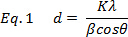
其中d为平均晶粒直径,K为材料的无量纲形状因子,β为X射线衍射(XRD)峰在布拉格角θ处的半高全宽。
扫描电子显微镜(SEM)用于监测退火薄膜中晶粒生长的程度(图 2B、C 和 图 3C-F)。在沉积单层 CdTe 或 CdSe 后,在 NH4Cl 存在下加热,可通过调节加热温度和时间、墨水浓度、喷涂压力/时间或旋涂速度来优化晶粒尺寸。通常,较大的晶粒表明器件具...
访问受限。请登录或开始试用以查看此内容。
讨论
综上所述,本实验方案提供了通过喷雾或旋涂沉积法制备溶液加工型电子器件的关键步骤指南。本文重点介绍了一种将透明导电的氧化铟锡(ITO)薄膜溶液加工沉积到非导电玻璃基底上的新方法。经过简单的刻蚀步骤后,可在喷雾沉积光敏层之前形成独立的电极。采用逐层沉积技术,可在环境空气条件下使用喷笔将CdSe和CdTe纳米晶体沉积成膜。经过配体交换和热处理后,最终的不透明导电金属电极可通过喷雾沉积在器件表面,并加热以去除原始有机配体。该电极层也可在沉积过程中通过使用掩模图案实现图形化。所制得的完全基于溶液加工的全无机器件可进行表征与性能测试。
应特别注意使用新鲜的试剂,因为过期的材料可能导致产物不纯或产生非预期产物。此外,在器件制备过程中应测试顶电极和底电极的导电性。ITO 薄膜的方块电阻应至少为 500 欧姆/方,顶部位金属薄膜的方块电阻应至少为 20 欧姆/方。如果方块电阻过高,应增加该电极的层数。当需要将多个器件串联或并联连接时,这一点尤为重要,因为每个器件都需要实现电子上的互连。应通过监控气压和墨水浓度变化的影响,严格控制各层的厚度和粗糙度。对这些薄膜进行轮廓仪扫描,可为喷雾或旋涂参数提供有价...
访问受限。请登录或开始试用以查看此内容。
披露
作者无任何利益冲突需要披露。
致谢
感谢海军研究办公室(ONR)提供的经费支持。本工作的部分内容是在汤森德教授于海军研究实验室担任美国国家研究委员会(NRC)博士后研究员期间完成的,同时感谢马里兰圣玛丽学院提供的内部支持。
访问受限。请登录或开始试用以查看此内容。
材料
| 姓名 | 公司 | 目录编号 | 评论 |
|---|---|---|---|
| 油酸,90% | Sigma Aldrich | 364525 | |
| 1-十八碳烯,90% | Sigma Aldrich | O806 | 技术级 |
| 三辛基膦(TOP),90% | Sigma Aldrich | 117854 | 对空气敏感 |
| 三甲基氯硅烷,99.9% | Sigma Aldrich | 92360 | 对空气和水敏感 |
| 硒,99.5%以上 | Sigma Aldrich | 209651 | |
| NH₄Cl4Cl,99% | Sigma Aldrich | 9718 | |
| CdCl2, 99.9% | Sigma Aldrich | 202908 | 剧毒 |
| CdO,99.99% | Strem | 202894 | 剧毒 |
| Te, 99.8% | Strem | 264865 | |
| In(NO₃)₃3)3.2.85H2O,99.99% | Sigma Aldrich | 326127-50G | |
| SnCl2.2H2O,99.9% | Sigma Aldrich | 431508 | |
| NH₄Cl4OH | Sigma Aldrich | 320145 | 腐蚀性 |
| NH₄Cl4否3, 99% | Sigma Aldrich | A9642 | |
| HAuCl4.3H2O,99.9% | Sigma Aldrich | 520918 | |
| 四辛基溴化铵(TMA-Br) | Sigma Aldrich | 294136 | |
| 甲苯,99.8% | Sigma Aldrich | 244511 | |
| 己硫醇,95% | Sigma Aldrich | 234192 | |
| NaBH₄4, 96% | Sigma Aldrich | 71320 | |
| 正己烷,98.5% | Sigma Aldrich | 650544 | |
| 乙醇,99.5% | Sigma Aldrich | 459844 | |
| 甲醇,无水,99.8% | Sigma Aldrich | 322415 | |
| 1-丙醇,99.5% | Sigma Aldrich | 402893 | |
| 2-丙醇,99.5% | Sigma Aldrich | 278475 | |
| 吡啶, > 99% | Sigma Aldrich | 360570 | 经蒸馏纯化 |
| 正庚烷 | Sigma Aldrich | 246654 | |
| 氯仿 > 99% | Sigma Aldrich | 372978 | |
| 丙酮 | Sigma Aldrich | 34850 | |
| 玻璃显微镜载玻片 | Fisher | 12-544-4 | 用玻璃刀切割 |
| 重力供料喷笔 | Paasche | VSR90#1 | |
| 注射器针头 | Fisher | CAD4075 | |
| 太阳能模拟器测试站 | 纽波特 | PVIV-1A | |
| 软件 | Oriel | 光伏IV 2.0 | |
| 圆底烧瓶 | Sigma Aldrich | Z723134 | |
| 圆底烧瓶 | Sigma Aldrich | Z418668 | |
| 聚四氟乙烯(PTFE)注射器滤器 | Sigma Aldrich | Z259926 | |
| 聚酰胺胶带 | Kapton | KPT-1/8 | |
| 玻璃纸胶带 | 苏格兰威士忌 | 810 胶带 | |
| 聚丙烯 离心管 | Sigma Aldrich | CLS430290 | |
| 银环氧树脂 | MG Chemicals | 8331-14G |
参考文献
- Debnath, R., Bakr, O., Sargent, E. H. Solution-processed colloidal quantum dot photovoltaics: A perspective. Energy Environ. Sci. 4, 4870-4881 (2011).
- Tang, J., Sargent, E. H. Infrared Colloidal Quantum Dots for Photovoltaics: Fundamentals and Recent Progress. Adv. Mater. 23, 12-29 (2011).
- Ning, Z., Dong, H., Zhang, Q., Voznyy, O., Sargent, E. H. Solar Cells Based on Inks of n-Type Colloidal Quantum Dots. ACS Nano. 8, 10321-10327 (2014).
- Yoon, W., et al. Enhanced Open-Circuit Voltage of PbS Nanocrystal Quantum Dot Solar Cells. Sci. Rep. 3, (2013).
- Jiaoyan, Z., et al. Enhancement of open-circuit voltage and the fill factor in CdTe nanocrystal solar cells by using interface materials. Nanotechnology. 25, 365203(2014).
- Kramer, I. J., et al. Efficient Spray-Coated Colloidal Quantum Dot Solar Cells. Adv. Mater. 27, 116-121 (2015).
- Shirasaki, Y., Supran, G. J., Bawendi, M. G., Bulovic, V. Emergence of colloidal quantum-dot light-emitting technologies. Nat. Photonics. 7, 13-23 (2013).
- Demir, H. V., et al. Quantum dot integrated LEDs using photonic and excitonic color conversion. Nano Today. 6, 632-647 (2011).
- Yu, G., et al. Solution-Processed Graphene/MnO2 Nanostructured Textiles for High-Performance Electrochemical Capacitors. Nano Lett. 11, 2905-2911 (2011).
- Ridley, B. A., Nivi, B., Jacobson, J. M. All-Inorganic Field Effect Transistors Fabricated by Printing. Science. 286, 746-749 (1999).
- Habas, S. E., Platt, H. A. S., van Hest, M. F. A. M., Ginley, D. S. Low-Cost Inorganic Solar Cells: From Ink To Printed Device. Chem. Rev. 110, 6571-6594 (2010).
- Townsend, T. K., Yoon, W., Foos, E. E., Tischler, J. G. Impact of Nanocrystal Spray Deposition on Inorganic Solar Cells. ACS Appl. Mater. Interfaces. 6, 7902-7909 (2014).
- Olson, J. D., Rodriguez, Y. W., Yang, L. D., Alers, G. B., Carter, S. A. CdTe Schottky diodes from colloidal nanocrystals. Appl. Phys. Lett. 96, 242103(2010).
- Sun, S., Liu, H., Gao, Y., Qin, D., Chen, J. Controlled synthesis of CdTe nanocrystals for high performanced Schottky thin film solar cells. J. Mater. Chem. 22, 19207-19212 (2012).
- Chen, Z., et al. Efficient inorganic solar cells from aqueous nanocrystals: the impact of composition on carrier dynamics. RSC Adv. 5, 74263-74269 (2015).
- Gur, I., Fromer, N. A., Geier, M. L., Alivisatos, A. P. Air-stable all-inorganic nanocrystal solar cells processed from solution. Science. 310, 462-465 (2005).
- Ju, T., Yang, L., Carter, S. Thickness dependence study of inorganic CdTe/CdSe solar cells fabricated from colloidal nanoparticle solutions. J. Appl. Phys. 107, (2010).
- MacDonald, B. I., et al. Layer-by-Layer Assembly of Sintered CdSexTe1-x Nanocrystal Solar Cells. ACS Nano. 6, 5995-6004 (2012).
- Crisp, R. W., et al. Nanocrystal Grain Growth and Device Architectures for High-Efficiency CdTe Ink-Based Photovoltaics. ACS Nano. 8, 9063-9072 (2014).
- Townsend, T. K., et al. Safer salts for CdTe nanocrystal solution processed solar cells: the dual roles of ligand exchange and grain growth. J. Mater. Chem. A. 3, 13057-13065 (2015).
- Jasieniak, J., MacDonald, B. I., Watkins, S. E., Mulvaney, P. Solution-Processed Sintered Nanocrystal Solar Cells via Layer-by-Layer Assembly. Nano Lett. 11, 2856-2864 (2011).
- Hecht, D. S., Hu, L. B., Irvin, G. Emerging Transparent Electrodes Based on Thin Films of Carbon Nanotubes, Graphene, and Metallic Nanostructures. Adv. Mater. 23, 1482-1513 (2011).
- Kim, M. G., Kanatzidis, M. G., Facchetti, A., Marks, T. J. Low-temperature fabrication of high-performance metal oxide thin-film electronics via combustion processing. Nat. Mater. 10, 382-388 (2011).
- Townsend, T. K., Foos, E. E. Fully solution processed all inorganic nanocrystal solar cells. Phys. Chem. Chem. Phys. 16, 16458-16464 (2014).
- Yu, W. W., Peng, X. Formation of High-Quality CdS and Other II-VI Semiconductor Nanocrystals in Noncoordinating Solvents: Tunable Reactivity of Monomers. Angew. Chem. 114, 2474-2477 (2002).
- Brust, M., Walker, M., Bethell, D., Schiffrin, D. J., Whyman, R. Synthesis of thiol-derivatised gold nanoparticles in a two-phase Liquid-Liquid system. J. Chem. Soc., Chem. Commun. 0, 801-802 (1994).
- Smits, F. M. Measurement of Sheet Resistivities with the Four-Point Probe. Bell Sys. Tech. J. 37, 711-718 (1958).
- Yoon, W., Townsend, T. K., Lumb, M. P., Tischler, J. G., Foos, E. E. Sintered CdTe Nanocrystal Thin-films: Determination of Optical Constants and Application in Novel Inverted Heterojunction Solar Cells. IEEE Trans. Nanotechnol. 13, 551-556 (2014).
- Foos, E. E., Yoon, W., Lumb, M. P., Tischler, J. G., Townsend, T. K. Inorganic Photovoltaic Devices Fabricated Using Nanocrystal Spray Deposition. ACS Appl. Mater. Interfaces. 5, 8828-8832 (2013).
- Nag, A., et al. Metal-free Inorganic Ligands for Colloidal Nanocrystals: S2-, HS-, Se2-, HSe-, Te2-, HTe-, TeS32-, OH-, and NH2- as Surface Ligands. J. Am. Chem. Soc. 133, 10612-10620 (2011).
- Panthani, M. G., et al. High Efficiency Solution Processed Sintered CdTe Nanocrystal Solar Cells: The Role of Interfaces. Nano Lett. 14, 670-675 (2014).
访问受限。请登录或开始试用以查看此内容。
重印与许可
