本文介绍了一种经过优化且基于实践经验的制备高质量石墨烯基莫尔超晶格器件的方案,该方案采用改进的干法转移技术,结合高度可调的自制转移装置,可精确控制扭转角度。
需要JoVE订阅才能观看此内容。 请登录或开始免费试用
本文内容
摘要
摘要
莫尔超晶格为研究强关联与拓扑效应相互作用所引发的新奇物态提供了一个多功能平台,同时具备灵活的原位可调性。然而,此类莫尔超晶格的制备具有挑战性。在纳米加工过程中,由于无意引入的异质应变、转角无序以及转角/晶格弛豫,难以实现具有精确转角的高均匀性器件。本文介绍了一种基于经验优化的高质量石墨烯基莫尔超晶格器件制备方案,重点采用了一种改进的干法转移技术。该转移过程在高度可调的定制化转移装置中进行,能够实现对位置、角度和温度的精确控制。通过结合严格的薄片筛选标准、预先清洗且无气泡的底部栅极,以及石墨烯激光刻蚀技术,可在室温下以亚微米级速度精确堆叠转角石墨烯薄片,从而构建莫尔超晶格。通过对转移过程的精确控制,所获得的石墨烯莫尔超晶格器件表现出高度均匀性和理想的转角。该优化方案解决了石墨烯基莫尔超晶格器件制备中的现有难题,为莫尔材料这一快速发展的领域进一步前进铺平了道路。
引言
现代凝聚态物理的一个关键驱动力是将强关联效应与拓扑性质结合到一个可调控的物理体系中。自从在魔角扭曲双层石墨烯(MATBG)中发现关联绝缘态1和超导性2以来,其显著的物理特性激发了人们对莫尔材料日益增长的研究兴趣3。近年来,多种基于石墨烯的莫尔超晶格结构已被构建并深入研究。这一快速发展的领域揭示了大量新奇的涌现现象,包括但不限于奇异的关联绝缘体4,5,6,7,8,9、非常规超导性10,11,12,13,14、向列性15以及轨道铁磁性16,17,18。
这些石墨烯莫尔超晶格中揭示的丰富物理现象得益于层间微小扭转角所带来的 unprecedented in situ 可调性。然而,这种额外的扭转角自由度也带来了不确定性。扭转角是通过将两片石墨烯以其晶轴相对旋转后堆叠而形成的。为了实现关联效应起主导作用的“魔角”区间(1°–1.2°),必须以优于0.1°的精度精确控制扭转角。但在器件制备过程中,可能引入多种不利因素,例如异质应变19,20、扭转角无序21,22,23以及晶格弛豫24,25等。使用质量不佳的石墨烯薄片或未能控制拾取石墨烯的速度,可能导致过大的应变和角度无序。由于小扭转角构型并非热力学基态,引入不必要的高温转移过程会增加晶格发生非预期弛豫的风险。这些因素降低了石墨烯莫尔超晶格器件制备的成功率,尤其在魔角区间表现更为显著。它们为此领域的研究人员带来了重大的实验挑战26,使得获得具有目标扭转角的器件变得困难,甚至难以重复先前的测量结果。
本文旨在缓解上述挑战,提供一种经过优化、基于经验且分步详尽的制备高质量石墨烯基莫尔超晶格器件的方案。该方案基于改进的干法转移技术27,28,采用一套高度可调、自行搭建的转移装置,实现对位置、角度和温度的精确控制。本方案的核心在于严格的薄片筛选标准、预先清洗且无气泡的底栅、石墨烯激光刻蚀,以及最重要的一点——在室温下以亚微米级速度平稳拾取预先切割的石墨烯薄片。除这些关键因素外,本文还讨论了可能影响实验结果的若干次要因素。尽管本方案以转角双层石墨烯为例进行说明,但其适用于所有类型的石墨烯基莫尔超晶格结构。该详细工作流程旨在提升高质量石墨烯莫尔超晶格器件制备技术在更广泛科研群体中的可及性。
访问受限。请登录或开始试用以查看此内容。
方案
本方案中使用的所有材料和仪器均可在材料表中找到。
1. 二维(2D)材料薄片的制备
- 石墨烯剥离
- 切割 Si/SiO2 使用碳化钨刻划笔将晶圆切割成 2 cm × 2 cm 的小片。随后用氮气喷枪清洁晶圆表面,以去除硅粉尘。
注意:带有285 nm厚SiO₂层的硅片2 通常用于石墨烯和hBN的剥离,因为该厚度可为二维材料的视觉识别提供良好的颜色对比度。 - 将加热板预热至 250 °C,然后将Si/SiO2 热板上的晶圆。
- 将石墨晶体置于无硅蓝色胶带(1005R)上。将胶带对折以覆盖晶体。用力按压石墨晶体,然后轻轻展开胶带。此操作可剥离石墨的顶层,暴露出平坦且有光泽的晶体表面。
- 将另一条矩形蓝色胶带贴在新剥离的石墨表面,轻轻按压后揭下,即可将新鲜石墨的顶层转移至新胶带上。
- 检查转移后的石墨层。晶体的量对于获得最佳剥离效果至关重要。如有需要,重复步骤 1.1.4 的操作,直至在新胶带上积累足够量的晶体(图1A).
- 轻轻折叠并展开新胶带多次,使石墨在胶带上均匀分布(图1B)。当表面被石墨薄层均匀覆盖时停止。
注意:过度折叠胶带可能会降低大片石墨烯碎片的产率。 - 在光源下检查新胶带(图1C)。理想情况下,胶带上应覆盖有透明的石墨小岛。如果胶带上存在过多较厚的石墨块,可在其上再贴一张蓝色胶带,撕下后有助于降低石墨的厚度。
- 将制备好的蓝色胶带裁剪成与Si/SiO尺寸相匹配的小片2 晶圆。将晶圆从加热板上取下,并立即贴上胶带。
- 让晶圆冷却至室温,然后轻轻剥离胶带。使用光学显微镜检查剥离效果。若晶圆表面残留过多胶带残留物,可考虑在下一次尝试中降低加热温度。
- 切割 Si/SiO2 使用碳化钨刻划笔将晶圆切割成 2 cm × 2 cm 的小片。随后用氮气喷枪清洁晶圆表面,以去除硅粉尘。
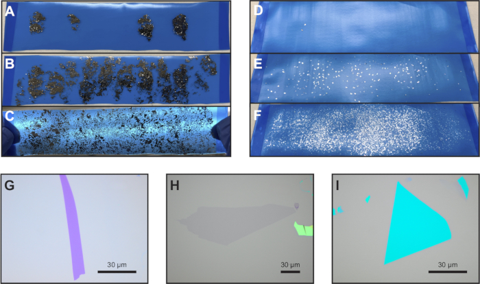
图 1:薄片剥离及选择标准。(A-C)石墨烯剥离。(A)将新转移的顶层石墨晶体置于新蓝色胶带上。(B)折叠并展开胶带,使石墨晶体在胶带表面分散开。(C)使用前将胶带朝向光源检查。理想情况下,大部分区域应被半透明的石墨岛覆盖。(D-F)六方氮化硼(hBN)剥离。(D)选取2至3颗有光泽的hBN晶体并放置在胶带上。(E)通过轻柔地折叠和展开胶带,使hBN晶体均匀分布在胶带表面。(F)使用前用反射光检查胶带表面。如果大部分晶体表面呈现彩色,则使用另一条胶带进一步减薄晶体。(G,H)符合薄片选择标准的典型二维材料薄片的光学显微图像,包括石墨指状结构(G)、单层石墨烯(H)和顶层hBN薄片(I)。(G,I)使用50倍物镜拍摄,而(H)使用100倍物镜拍摄。所有比例尺均为30 µm。请点击此处查看该图的放大版本。
- 六方氮化硼(hBN)剥离
- 按照步骤 1.1.1 中所述切割并清洗晶圆。将加热板预热至 160 °C.
- 将2-3个有光泽的hBN晶体置于一块矩形无硅蓝色胶带(1009R)上(图1D).
注意:石墨烯和六方氮化硼(hBN)的剥离使用不同的胶带。1005R 胶带比 1009R 具有更强的粘附性,导致晶片上的薄片密度更高,但胶带残留物也更多。 - 轻轻折叠并展开胶带数次,使六方氮化硼(hBN)晶体在胶带表面均匀分布(图1E当胶带表面覆盖上薄而闪亮的hBN晶体时停止。
- 在反射光下检查胶带表面(图1F)。如果厚晶体过多,按照步骤1.1.7所述,使用另一条蓝色胶带降低其厚度。
- 将制备好的蓝色胶带裁剪成与 Si/SiO 尺寸相同的片状2 晶圆。在室温下将胶带平滑地贴附到晶圆上。
- 将粘贴好的晶圆置于加热板上 160 °C 加热2分钟。加热后,待晶圆冷却至室温,以每片晶圆约2分钟的缓慢且受控的速度小心剥离胶带。
- 去除胶带后,将晶圆放入炉内石英管中进行退火处理 350 °C 在形成气体环境(50% H₂)中持续10小时2- 50% Ar)。此步骤旨在减少晶圆表面的胶带残留物。
注:其他退火条件(如高真空)也可获得类似结果。 - 退火过程完成后,将晶圆从炉中取出,并使用氮气喷枪吹去退火过程中引入的任何玻璃颗粒。
- 退火石英管 1000 °C 暴露于空气中1小时。此步骤可去除管内的化学残留物,为后续退火过程做准备。
- 二维材料的薄片选择
- 对于二维材料薄片的筛选,使用配备5倍物镜的光学显微镜,在明场照明下快速预筛晶圆。根据讨论部分所述的薄片筛选标准,识别出符合所需尺寸、形状和厚度的薄片。符合标准的代表性薄片如图所示 图1G - I.
- 使用50倍或100倍物镜,通过调节明场图像的色彩对比度来评估薄片质量。或者,采用暗场照明并设置足够的曝光时间以检查薄片。这两种方法均有助于进一步剔除不完整的薄片。
- 为验证薄片质量,建议采用轻敲模式原子力显微镜(AFM)检测薄片表面形貌。仅选择表面洁净且无明显应变的薄片进行后续处理。
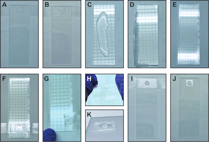
图 2:带有 PC/PDMS 印模的玻璃片的制备。(A)将带有打孔的双面胶带粘附在玻璃片的一端。(B)将一块洁净的 PDMS 印模置于打孔的中心位置。(C)将适量的溶于氯仿中的 PC 溶液滴加到玻璃片上。(D)将另一块洁净的玻璃片覆盖在下方的玻璃片上,以均匀铺展溶液,并使两块玻璃片相互滑动。(E)氯仿挥发后,在下方玻璃片上形成一层均匀的 PC 薄膜。(F)将另一片带有打孔的双面胶带贴在 PC 薄膜的洁净区域上。使用镊子背面在孔周围划出划痕,以确保胶带与 PC 薄膜之间紧密结合。(G)沿胶带边缘切割 PC 薄膜并轻轻剥离。(H)在孔的中心位置可见一片自支撑的均匀 PC 薄膜。(I)通过将(H)中的打孔与(B)中的打孔对齐,将自支撑的 PC 薄膜覆盖到 PDMS 印模上。将孔周围的双面胶带紧密压合。(J)切除多余的胶带,仅保留中央的 PC/PDMS 印模区域。(K)PC/PDMS 印模的放大视图。请点击此处查看该图的放大版本。
2. 使用聚碳酸酯/聚二甲基硅氧烷印章制备玻片
- 使用聚碳酸酯(PC)和聚二甲基硅氧烷(PDMS)印章制备玻璃载玻片,用于转移二维材料。
- 准备一个洁净的6英寸培养皿。将硅弹性体基质与固化剂按10:1的质量比在培养皿中混合。为获得约1–2 mm的适宜PDMS厚度,通常使用约10 g基质和1 g固化剂的混合物。
- 充分混合后,将培养皿置于平坦表面,在室温下固化2天。固化完成后,PDMS即可使用。
- 将带有通孔的双面胶带贴在洁净玻璃载玻片的一端(图2A)。然后,将一块洁净的PDMS印章(厚度1–2 mm)置于孔的中央(图2B)。
注意:为确保PDMS印章与玻璃载玻片之间具有良好的粘附性,界面必须洁净、均匀,且无灰尘或气泡。 - 在通风橱中,取另一块洁净的玻璃载玻片,并在其表面滴加适量6% w/w的PC氯仿溶液(如图2C所示)。
- 将另一块洁净的玻璃载玻片盖在下方的载玻片上并轻轻按压(图2D)。待溶液铺展后,将两块玻璃载玻片相对滑动,以形成均匀的PC薄膜。待氯仿完全挥发后,底部载玻片上即形成一层PC薄膜(图2E)。
- 在PC薄膜表面洁净且均匀的区域,覆盖另一块带有通孔的双面胶带。使用镊子背面在孔周围按压,确保胶带与PC薄膜牢固粘合(图2F)。
- 沿胶带边缘切割PC薄膜,将该部分从载玻片上的其余部分分离,然后轻轻揭下胶带(图2G)。
- 揭下胶带后,检查孔中央自支撑的PC薄膜(图2H)。建议在高湿度环境中制备PC薄膜,例如雨天。否则,薄膜在揭离过程中可能出现褶皱。若出现褶皱,需重复步骤2.1.6–2.1.7,直至获得均匀的PC薄膜。
- 将自支撑的PC薄膜覆盖到步骤2.1.3中制备的PDMS印章上。然后使用剃刀刀片在通孔周围用力按压双面胶带,使其牢固贴合(图2I)。
- 剪除中心PC/PDMS印章区域以外多余的胶带。至此,一端带有PC/PDMS印章的玻璃载玻片制备完成(图2J),其局部放大图如图2K所示。
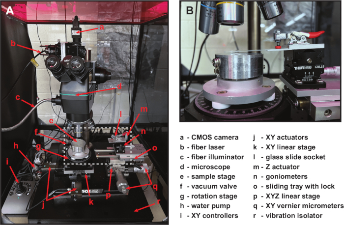
图3:高度可调的定制转移装置。(A)转移装置的前视图,关键组件以红色箭头和字母标注,各组件名称列于右侧。装置的核心区域由灰色虚线框标出。(B)(A)中核心区域在预接触状态下的放大视图,显示PC/PDMS印章位于Si/SiO2晶圆上方约2 mm处。请点击此处查看此图的放大版本。
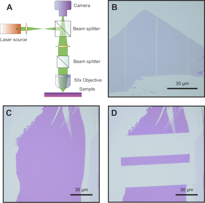
图4:石墨烯激光烧蚀。(A)定制转移装置中激光光路的示意图。激光束与相机成像光路共焦,以实现精确的激光烧蚀。(B)激光烧蚀后的单层石墨烯薄片。中间的激光切割线被切割两次,以增加相邻石墨烯片之间的间隙,而两条外侧切割线则将核心区域与薄片其余部分分离。(C)一片厚度均匀但形状不规则的石墨薄片。(D)激光烧蚀将不规则的石墨加工成矩形石墨指状结构,使其非常适合作为石墨栅极电极使用。所有比例尺均为30 µm。(A)改编自 Park 等人38。请点击此处查看该图的放大版本。
3. 二维材料莫尔超晶格的干法转移(以转角双层石墨烯为例)
注意:有关本实验方案中使用的定制转移装置(图3A)和集成超连续谱激光器(图4A)的详细信息,请参见讨论部分。
- 石墨烯激光烧蚀
- 将石墨烯晶圆放置在样品台上,使用10倍物镜定位石墨烯。调整石墨烯薄片至所需方向,然后切换至50倍物镜。
- 在 Inkscape 中使用绘制贝塞尔曲线和直线功能,勾勒出石墨烯的边界以及规划的激光切割线。如果石墨烯存在轻微褶皱或裂纹区域,请使用激光切割线将其与核心区域分离,以降低在拾取石墨烯过程中进一步发生折叠或开裂的风险。
注意:激光切割线可根据目标结构将石墨烯分割为两个或多个部分,每部分宽度至少为20 µm,长度至少为30 µm。 - 开启激光器并逐渐增加激光强度,直至光斑可见。调节样品台,使光斑对准规划切割线的起点,然后将激光强度调节至适合石墨烯烧蚀的水平。
注意:在不损伤SiO2表面的前提下,切割石墨烯所需的激光功率为60 mW至150 mW(在分束器前测量)。 - 移动样品台,引导光斑沿规划的激光切割线行进,完成薄片切割。切割完成后,将激光强度归零,并检查切割线质量。
- 重复上述操作,在已有切割线附近进行额外一次切割。这可以增大石墨烯各部分之间的间隙,为hBN直边对准时提供更大空间,避免与相邻石墨烯部分接触。
- 对每一条规划的激光切割线重复该操作。完成激光烧蚀后,原始石墨烯被分割成多个部分(图4B),用于构建莫尔超晶格的中心部分已与其他区域隔离。
- 将石墨烯晶圆从样品台上取下,并使用光学显微镜检查激光切割线,确保切割线区域无任何污染物。
注意:石墨烯激光烧蚀技术也可用于将石墨薄片加工成所需几何形状。例如,可将不规则的石墨薄片(图4C)加工成理想的矩形石墨指状结构(图4D),适用于作为栅极电极。该方法显著减少了寻找特定几何形状石墨薄片所需的时间。
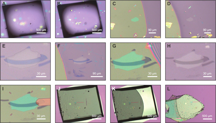
图 5:底部石墨栅极的转移。(A)对准 PC 薄膜,并在 2 倍物镜下识别出一个洁净区域。(B)对准 hBN 薄片并将其移至(A)中识别出的洁净区域。(C)印章与晶圆接触,形成浅绿色接触区域,其彩色右边缘称为波阵面。PC 薄膜完全覆盖底部 hBN 薄片。(D)底部 hBN 薄片被拾取,薄片颜色呈半透明状。(E)在印章接触晶圆之前,将 hBN 与石墨指状电极进行最终对准。(F)波阵面接近石墨指状电极,此时结合速度降低至 0.5 µm/s。(G)波阵面完全通过石墨指状电极。(H)底部 hBN 薄片拾取石墨指状电极。(I)在 160 °C 下将底部石墨栅极释放到预图案化的标记晶圆上,确保石墨指状电极与 Ti/PdAu 金属指状电极之间形成接触。(J)将整个 PC/PDMS 印章压合到晶圆上。(K)PC 薄膜从 PDMS 印章上分离。不同颜色区域之间的透明波阵面表明 PC 薄膜与 PDMS 印章之间发生剥离。(L)PC 薄膜从玻璃载片上撕下,将底部石墨栅极留在晶圆上。图(A,B,J,K,L)中的比例尺为 500 µm;图(C,D,F)中为 90 µm;图(E,G,H,I)中为 30 µm。请点击此处查看该图的放大版本。
- 制备石墨底栅
- 按照步骤 3.3 中的类似步骤拾取底 hBN 薄片(图 5A – D)。需要注意的是,对于底 hBN 薄片,无需具有直的晶边和平行的波阵面(波阵面的定义见步骤 3.3.8)。
- 将带有石墨指状电极的晶圆放置在样品台上。将石墨指状电极置于相机视窗中央,并将其方向调整至所需方向。使用 Peek Through 功能使 Inkscape 窗口在相机视窗上方浮动时呈现半透明状态。在 Inkscape 中勾勒出石墨指状电极的边界。
- 将样品台温度设定为 80 °C。装载玻璃载片并将其移至预接触位置(参见步骤 3.3.4 和 图 3B)。
- 按照 3.4.5–3.4.10 中所述的类似步骤,在 stamp 接触晶圆之前对齐底 hBN 薄片和石墨指状电极,如 图 5E 所示。此对齐可确保石墨指状电极位于底 hBN 薄片的洁净且均匀区域下方。
- 使用 Z 方向驱动器以 5 µm/s 的速度将 PC/PDMS stamp 接触到晶圆上,直至波阵面接近石墨指状电极(图 5F)。
- 将速度降低至 0.5 µm/s,使波阵面缓慢通过石墨指状电极,直到完全覆盖石墨(图 5G)。
- 以 0.5 µm/s 的速度撤回波阵面。一旦石墨指状电极被拾取,其颜色将从紫色变为半透明的深灰色(图 5H)。当石墨完全被拾取后,以 5 µm/s 的速度完全撤回波阵面。
- 在样品台温度为 160 °C 的条件下,将底 hBN 薄片和石墨栅极热释放到预图案化的标记晶圆上,使其接触 Ti/PdAu 金属指状电极(图 5I–L),操作步骤与步骤 3.5 中所述类似。
- 将晶圆浸入氯仿中一小时以去除 PC 膜。去除后,用异丙醇冲洗晶圆,并用氮气喷枪吹干。
注意:通常情况下,20 分钟的氯仿处理足以溶解 PC 膜。此处使用 1 小时以获得更洁净的栅极表面。 - 将晶圆放入石英管中,在成形气体气氛(50% H2–50% Ar)下于 350 °C 退火 10 小时。
- 使用光学显微镜检查底栅。无气泡的底部石墨栅极的明场和暗场显微图像如 图 6A、B 所示。
- 使用 AFM 轻敲模式扫描底栅。选择无气泡且结构均匀的栅极区域,所选区域宽度略大于栅极宽度。退火后的栅极表面覆盖有聚合物残留物,如 图 6C 所示。
- 在选定均匀且无气泡的栅极区域后,将 AFM 切换至标准接触模式,使用上一步中相同的轻敲模式探针。
注意:轻敲模式探针比接触模式探针更刚硬,可获得更好的清洁效果。 - 以每扫描 512 行的分辨率扫描选定区域,并以约 20 µm/s 的速度在探针尖端施加数十 nN 的法向力,以清除表面的聚合物残留物。该步骤称为探针清洁过程。
- 完成一轮探针清洁后,将 AFM 切回轻敲模式,并使用新的轻敲模式探针检查清洁效果。
- 重复探针清洁过程,直至聚合物残留物从栅极区域完全清除至边缘(图 6D)。
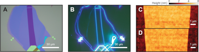
图6:预清洁且无气泡的底部石墨栅极。(A,B)典型无气泡底部石墨栅极的光学显微镜明场(A)和暗场(B)图像。原子力显微镜(AFM)显示尖端清洁工艺前脏污栅极表面(C)和清洁后洁净栅极表面(D)的形貌图像。聚合物残留物被扫至一侧,形成两条垂直线,如图(D)所示。图(A,B)中的标尺为30 µm,图(C,D)中的标尺为1 µm。请点击此处查看该图的放大版本。
- 拾取顶部的 hBN 薄片
- 将晶圆放置在样品台上,使用 10 倍物镜定位顶部的 hBN 薄片。
- 调整 hBN 薄片的方向,使其直边垂直并对准薄片右侧。然后在 Inkscape 中勾画出薄片的边界。该图形将作为后续将 hBN 与石墨烯薄片对准的参考依据。
注意:在整个转移过程中,相机与 Inkscape 的缩放倍数必须保持一致,以确保薄片与图形之间的比例统一。 - 将带有 PC/PDMS 转印膜的载玻片轻轻夹入插槽中,保持向下倾斜 2°–3° 的角度。通过滑动托盘将插槽向左移动,直至载玻片位于样品晶圆上方,然后手动锁定其位置。
- 将样品台温度设定为 50 °C。使用 Z 向驱动器以 1 mm/s 的快速度将载玻片向下推进,直至转印膜距离晶圆表面 2 mm。此时系统处于预接触位置(图 3B)。
- 将显微镜聚焦于 PC 膜表面,检查其清洁度(类似于 图 5A)。在转印膜中心略偏左的位置选择一个洁净区域用于接触 hBN 薄片,因为转印膜将从左侧接触。移动 hBN 薄片,使其对准所选洁净区域。
- 继续以 0.1 mm/s 的速度将载玻片向下推进。当 PC 膜与晶圆接近同一焦平面时,将速度降低至 5 µm/s。
- 通过观察转印膜与晶圆之间形成的牛顿环来确定接触点。为确保拾取过程平滑,需确保 hBN 薄片位于接触点右侧并远离该点。若不符合此条件,则返回预接触位置,并重复步骤 3.3.5–3.3.7 以调整 hBN 的位置。
- 当转印膜接触晶圆时,其界面会呈现绿色接触区域,其彩色的右边缘称为波前。如 图 7A 所示,平行的波前更容易在 hBN 的直边处被固定。
注意:由于转印膜表面可能存在轻微倾斜,波前相对于 hBN 直边可能略有倾斜。为确保在拾取石墨烯时两者平行,请记录大致的倾斜角度,并记住在步骤 3.4.3 中使用倾角调节器进行补偿。 - 以 5 µm/s 的速度进一步将转印膜压向晶圆,直至完全覆盖 hBN 薄片(类似于 图 5C)。随后将样品台温度设定为 80 °C。
注意:若 PC 膜的粘附性不确定,可先将样品台温度设为 60 °C,然后逐步升高温度,直至 hBN 能够顺利被拾取。 - 达到设定温度后,以 5 µm/s 的速度撤回转印膜,直至波前接近 hBN 的直边。随后将速度降至 2 µm/s,缓慢拾起 hBN 薄片。一旦完成拾取,将速度提高至 5 µm/s,使 PC 膜完全脱离晶圆。
注意:当回撤的波前触及 hBN 直边时,需仔细观察薄片颜色变化。成功拾取后,薄片将变为透明。若薄片仍呈现彩色,则重新压下转印膜覆盖薄片,并在更高温度下重复上述步骤。随着温度升高,PC 膜对薄片和晶圆的粘附性均会增强。建议最高温度不超过 120 °C。超过 120 °C 可能导致在撤回过程中 PC 膜从 PDMS 转印膜上脱落。若 PC 膜粘性不足,可考虑对带有转印膜的载玻片进行 5–10 分钟的紫外/臭氧处理。该处理可增强 PC 膜对二维材料的粘附性,提高薄片拾取的成功率。 - 关闭样品台加热器并开启水冷系统。待温度降至 45 °C 以下后,关闭水冷系统,并以 1 mm/s 的速度将载玻片完全撤回至最高位置。从样品台上取下 hBN 晶圆。
注意:高温下剧烈移动载玻片会扰动脆弱的薄片,可能导致冷却后出现褶皱或裂纹。若出现严重褶皱或裂纹,应弃用该薄片,因为这些不平整结构会阻碍石墨烯的顺利拾取。
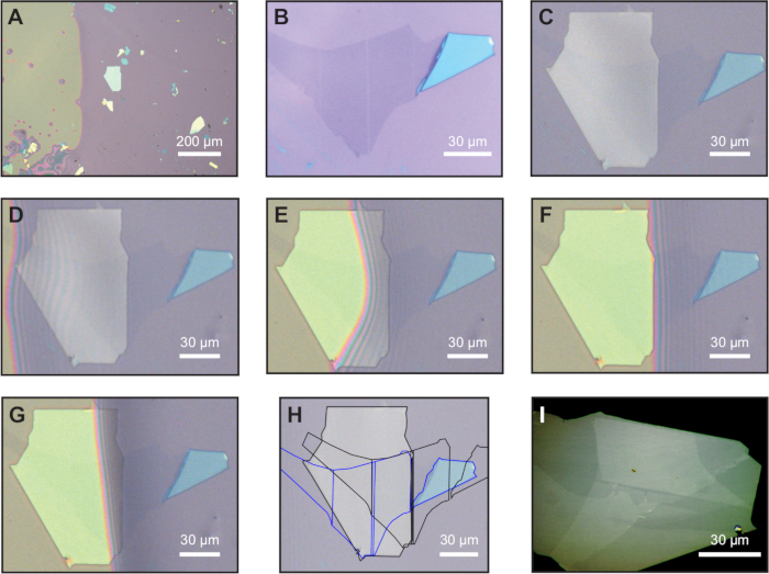
图7:石墨烯莫尔超晶格转移过程中的关键步骤。(A)拾取顶部六方氮化硼(hBN)薄片前拍摄的宏观图像。聚碳酸酯/聚二甲基硅氧烷(PC/PDMS)印章与晶圆之间的接触区域呈浅绿色。值得注意的是,波阵面与顶部hBN薄片的直边平行。(B)激光烧蚀后的石墨烯薄片。中间的激光切割线将第一块和第二块石墨烯分隔开,由于进行了两次切割,这两块石墨烯更宽,如步骤3.1.5所述。另外两条切割线用于将石墨烯核心区域与长石墨烯尾部及较厚的石墨块分离,若不分离,这些部分可能在拾取过程中引入额外应变。(C)在拾取第一块石墨烯之前,hBN与石墨烯已处于最终对准位置。(D)波阵面非常接近hBN左侧边缘,此时应将接触速度降低至0.02 µm/s。(E)hBN缓慢接触第一块石墨烯。(F)波阵面完全越过第一块石墨烯,并被hBN的直边钉扎。(G)hBN正在平稳拾取石墨烯。(H)在拾取第二块石墨烯之前,各薄片已与各自的示意图对齐。hBN和原始石墨烯示意图的边界以黑色标出,而旋转后复制的石墨烯示意图则以蓝色表示。(I)通过(A–H)步骤制备的顶层堆叠结构的光学显微图像,颜色对比度经过优化,以清晰显示堆叠内部的精细特征。仅观察到极少的无序结构,表明该顶层堆叠为高质量的转角双层石墨烯。所有图像中的比例尺均为30 µm,仅(A)中为200 µm。请点击此处查看该图的放大版本。
- 拾取石墨烯莫尔超晶格
- 将带有新近激光切割石墨烯的晶圆放置在样品台上。使用10倍物镜定位石墨烯,然后调整石墨烯片层的取向,使激光切割线与六方氮化硼(hBN)的直边平行,如图所示。 图7B.
- 勾勒石墨烯边界 Inkscape,包括激光切割线。使用 窥探 使绘图在相机窗口上方浮动时呈现半透明效果。
- 根据步骤 3.3.8 的观察结果,调节测角仪以补偿波前与 hBN 直边之间的倾斜。
- 将带有顶部hBN薄片的玻璃载玻片装载到位,并将其移至预接触位置,使PC/PDMS印章位于石墨烯晶圆上方2 mm处。
- 将 hBN 和石墨烯的示意图对齐,使 hBN 的直边位于激光切割线的中央,该切割线用于分隔中心的石墨烯部分。调节显微镜以聚焦在石墨烯上,然后将其与示意图对齐 Inkscape.
- 聚焦顶部的hBN薄片,移动玻璃载片的XY方向,使hBN与其示意图对齐。此步骤完成预接触位置的粗略对准。
- 聚焦于预先切割的石墨烯,然后略微向上调整焦平面。以0.1 mm/s的速度将玻璃载片向下移动,直至顶部的六方氮化硼(hBN)薄片进入焦点。此时,hBN与预先切割的石墨烯已非常接近。
- 重新聚焦到石墨烯上。将速度设置为 5 µm/s 缓慢压下印章,直至六方氮化硼(hBN)大致可见,确保印章与晶圆不发生接触。
- 将石墨烯和顶部的hBN均重新对准至其对应的标记图形。这一步将作为 stamp 接触晶圆前的最终对准。如图所示,薄片已实现良好对准。 图7C.
注意:一旦印章接触晶圆,应避免进一步的对准调整。移动印章可能会在PC薄膜和hBN中引入过大的应变。 - 继续向下按压印章,直至其接触晶圆。如果波阵面仍不平行于hBN的直边,则从步骤3.4.3重新开始,以重新调整测角仪。目标是实现如图所示的平行波阵面 图7A.
- 通过持续向上移动印模并同时监测波前运动,评估 z 轴平台的滞后水平。若波前先向前移动数个单位 µm 然后开始回缩,表明该载物台在此玻片上表现出明显的滞后现象;反之,如果波阵面立即回缩而无任何向前移动,则表明该载物台在此玻片上无明显滞后现象。
注意:迟滞效应可能影响波阵面在hBN直边处的钉扎,导致过度接触,从而污染后续的石墨烯样品。因此,若观察到迟滞效应,建议后续接触过程优先采用直流电流加热法(步骤3.4.13),而非机械法(步骤3.4.12)。 - 机械法(无滞后):使用 5 µm/s 速度推动印章,直至波前接近六方氮化硼(hBN)的左边缘图7D)。将速度降低至 0.02 µm/s,然后使用此极慢速度将hBN与第一片石墨烯接触(图7E)。一旦它完全覆盖第一片石墨烯并被固定在六方氮化硼的直边上(图7F),停止 engagement 过程。以一定速度向上移动载物台以消除滞后现象 5 µm/s 直到波前趋于回缩。
注意:需密切监控缓慢接触过程,因为如果未在 hBN 直边处及时停止,波阵面可能会过度接触并污染下一个石墨烯样品。 - 直流电流加热法(带滞后):使用 5 µm/s 速度推动印章,直至波前接近六方氮化硼(hBN)的左边缘图7D)。通过向上移开印章以消除滞后现象,直至波阵面开始回缩。对样品台加热器施加微小的直流电流,以缓慢且可控地加热样品台,升温速率为0.5-1 °C/分钟
注意:由于印章的热膨胀,波前将持续接触图7E)。一旦它完全覆盖第一片石墨烯并被固定在六方氮化硼的直边缘处(图7F),停止直流电流。 - 设定一个脱离速度 0.02 µm/s 轻轻地拾取石墨烯(图7G)。等待波前移出六方氮化硼(hBN)后,再提高速度 5 µm/s 完全将印章从晶圆上剥离。
- 当印章与晶圆完全分离后,将印章以额外3秒的时间向上移动 5 µm/s 速度需适中,以确保所有薄片均从PC膜或晶圆上完全脱离。否则,一旦发生扭转,将导致PC膜起皱。
- 复制整个石墨烯图案 Inkscape 并将其旋转至所需扭转角度(±1.13° 用于MATBG)。将复制的图改为不同颜色以避免混淆(如蓝色) 图7H将复制图中的第二片石墨烯与原始图中的第一片石墨烯对齐,使其重叠部分最大化。
注意:根据经验,装置中的最终扭转角度通常小于转移过程中设定的目标角度。因此,该角度通常需略微设高一些(约 0.05°)而非“魔角”,这正是选择±1.13° 用于MATBG器件的制备。 - 将样品台旋转至所需扭转角度(±1.13° 用于MATBG。将晶圆上剩余的石墨烯与复制的石墨烯图形对齐。精确的扭转角度控制通过旋转台中的直流伺服电机实现,该电机提供 360° 连续旋转,使用 2 µrad 分辨率高且滞后效应可忽略。
- 聚焦玻璃载片上的顶部hBN薄片,并将其与图纸对齐。由于hBN与剩余的石墨烯已处于紧密接近的位置,此对齐即作为最终对齐步骤。图7H).
- 重复步骤 3.4.12–3.4.14 以拾取扭曲的石墨烯片。如果这是最后一个待拾取的石墨烯片,波前可越过 hBN 的直边过度接触,从而更彻底地挤出堆叠内部的气泡。
- 此时,石墨烯莫尔超晶格已完全被顶部 hBN 薄片拾取,整体称为顶部堆叠体。
- 使用光学显微镜检查顶层堆叠的质量。保存具有颜色对比的明场图像,供步骤3.5.2使用。 图7I高质量的双层石墨烯上层堆叠样品,可见气泡极少。
- 封装石墨烯莫尔超晶格
- 将带有预先清洁且无气泡的底栅的晶圆放置在样品台上。使用10倍物镜定位底栅。
- 将顶部图层的彩色对比明场图像导入 Inkscape 将其与图纸对齐,定位并勾勒出顶层堆叠中无气泡石墨烯莫尔超晶格区域的边界,该区域将覆盖在底栅上。
- 调整栅极方向,以覆盖无气泡上层堆叠的最大面积。然后,勾勒出底部栅极的边界。
- 封装完成后,将样品台温度设置为以撕下PC膜 160 °C,高于PC的玻璃化转变温度(147 °C).
- 将顶部堆栈加载到玻璃载玻片上,然后移至预接触位置。根据图纸大致对齐底部栅极和顶部堆栈。
- 聚焦于底栅,然后略微提升焦平面。以0.1 mm/s的速度将玻璃载玻片向下推进,直至顶部堆叠结构在焦平面中可见。
- 在底部门和顶层堆栈之间确定另一个中间焦平面。将速度设置为 5 µm/s 逐渐压下印模,直至顶部堆叠显现。
注意:在温度高于 120 °C一旦印章与晶圆接触,便很难将二者分离。以中间焦平面作为参考,可确保印章与晶圆在达到最佳对准之前不会发生接触。 - 重复步骤 3.5.7,直至底部门极与顶层堆叠几乎处于同一焦平面,准确对准图纸。此步骤作为印章接触晶圆前的最终对准。同时,样品台到达约 160 °C.
注意:高温会引起空气对流,导致相机图像抖动,从而增加精确对准的难度。然而,为防止热诱导的转角弛豫,必须尽快完成对准。因此,该操作需要大量练习。 - 使用一个速度 5 µm/s 将印章压下直至接触晶圆。当波阵面接近底部门极时,降低速度至 0.5 µm/s.
- 缓慢将顶层堆栈与底层栅极接合。当波阵面通过顶层堆栈后,切换回 5 µm/s 将整个印章完全压接到晶圆上(类似于 图5J).
注意:在堆叠顶层时需仔细控制波前。平稳的操作过程有助于提高最终堆叠中维持目标扭转角度的可能性。 - 等待1分钟,以确保PC膜完全软化,然后以一定速度分离印章 5 µm/sPC薄膜仍附着在晶圆上,而PDMS印章回缩,在两者之间形成一个透明的波前(类似于 图 5K).
- 波前完全回缩后,PC薄膜与PDMS印章将彻底分离。以指定速度向上提起印章,持续额外3秒 5 µm/s,然后开始移动它以撕下PC膜(类似于 图5L).
- 撕下PC薄膜后,以1 mm/s的速度完全分离玻璃载片,然后将其从卡槽中取出。关闭载物台加热器并启动水冷系统。待载物台冷却至室温后,取下晶圆,使用光学显微镜检查封装的石墨烯莫尔超晶格。
4. 石墨烯莫尔超晶格器件的霍尔棒几何结构定义
- 将晶圆浸入氯仿中 20 分钟以去除 PC 薄膜。从氯仿溶液中取出后,用异丙醇冲洗晶圆一次,并用气流吹干。
- 再次使用光学显微镜检查堆叠结构,确保在去除 PC 薄膜后结构保持不变。然后使用原子力显微镜轻敲模式扫描封装的石墨烯莫尔超晶格。选择无气泡、无裂纹且无张力的区域作为目标器件区域。该过程可滤除高度无序的区域,提高不同样品间扭转角的一致性。
- 采用电子束光刻(EBL)定义接触电极构型,随后使用反应离子刻蚀(RIE)结合标准 hBN 刻蚀工艺(CHF3 与 O2 混合气体)暴露新鲜的石墨烯边缘。刻蚀完成后立即进行 Cr/Au 一维边缘电极的热蒸发沉积29。
- 使用 EBL 和 RIE 定义最终的霍尔棒器件几何结构。至此,完成石墨烯莫尔超晶格器件的制备过程。
访问受限。请登录或开始试用以查看此内容。
结果
为表征石墨烯莫尔超晶格器件,进行了低温输运测量。以魔角扭曲双层石墨烯(MATBG)为例,图8A22展示了一个高质量魔角器件典型的朗道扇形图。平带的填充因子ν = 4n/ns 用于描述系统的载流子密度,其中n为载流子密度,ns = 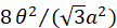 为超晶格密度(
访问受限。请登录或开始试用以查看此内容。
讨论
在石墨烯层之间引入微小的扭转角度可能会在异质结构中产生显著的无序。因此,为了最大限度地提高制备高质量石墨烯莫尔超晶格器件的成功率,必须使用一种高度可调的转移装置,以实现对位置、角度和温度的精确控制。此外,在制备过程中还需关注若干关键因素:严格的薄片筛选标准、预先清洗且无气泡的底层栅极、石墨烯激光刻蚀,以及最重要的一点——在室温下以亚微米速度平稳拾取预先切割的石墨烯碎片。
本方案中的转移过程是在一个高度可调的定制转移装置中进行的,如图所示 图3A整个装置安装在被动式隔振器上,以最大限度减少振动噪声。使用配备2倍、10倍和50倍长工作距离物镜的显微镜观察转移过程,并连接CMOS相机至计算机。样品台基于直驱旋转台,可实现360°连续旋转,分辨率为2 µrad,配备水冷系统和中心真空接口以固定晶圆。此外,该样品台还可在XY方向移动,由两个微线性驱动器控制。带有PC/PDMS印章的玻璃载片可牢固地夹紧在插座中图3B),倾斜角度可通过底部的两个测角仪进行调节。该插座安装在一个...
访问受限。请登录或开始试用以查看此内容。
披露
作者声明无利益冲突。
致谢
作者们衷心感谢Jarillo-Herrero课题组所有现任和前任成员在开发和优化制备方案方面所做的贡献。本工作主要由美国陆军研究办公室MURI项目(W911NF2120147)资助,同时得到了2DMAGIC MURI项目(FA9550-19-1-0390)、麻省理工学院/微系统技术实验室三星半导体研究基金、Sagol WIS-MIT桥梁计划、美国国家科学基金会(DMR-1809802)、戈登与贝蒂·摩尔基金会EPiQS计划(资助号GBMF9463)以及拉蒙·阿塞斯基金会的资助。本研究利用了哈佛大学纳米系统中心的设施,该中心由美国国家科学基金会(ECS-0335765)支持。
访问受限。请登录或开始试用以查看此内容。
材料
| 姓名 | 公司 | 目录编号 | 评论 |
|---|---|---|---|
| 台式振动隔离平台 | Minus K Technology, Inc | 100BM-8 | 定制转移装置的振动隔离 |
| 彩色相机 | Teledyne FLIR LLC | BFS-U3-200S6C-C | 用于定制转移装置的CMOS相机 |
| 隔膜泵 | Pfeiffer Vacuum | MVP 015-2 | 为样品台上的晶圆提供真空吸力以将其固定 |
| 直接驱动旋转台 | Thorlabs, Inc | DDR 100 | 用于定制转移装置的旋转台 |
| 符合人体工学的高功率显微镜 | Mitutoyo | FS70 | 用于定制转移装置的显微镜主体 |
| 测角仪载物台 | Thorlabs, Inc | GNL 18 和 GNL 10 | 控制玻璃载片的倾斜角度 |
| 石墨晶体 | NGS 交易 & Consulting GmbH | 荧光薄片 | 用于石墨烯剥离的扁平有光泽石墨晶体 |
| 高功率超连续谱光纤激光器 | Fianium, Inc | SC-400 | 用于石墨烯激光烧蚀 |
| 内置控制器的微型线性执行器 | Zaber Technologies | X-NA08A25 | 控制 X-Y 样品台 |
| Mitutoyo 10倍M Plan APO物镜 | Mitutoyo | 378-803-3 | 转移阶段使用的10倍物镜 |
| Mitutoyo 2x M Plan APO 物镜 | Mitutoyo | 378-801-12 | 转移阶段使用2x物镜 |
| Mitutoyo 50倍 M Plan APO 物镜 | Mitutoyo | 378-805-3 | 转移阶段使用的50倍物镜 |
| 电动执行器 | Zaber Technologies | TRB12CC | 控制 X-Y-Z 玻璃载物片支架平台 |
| 聚(双酚A碳酸酯) | MilliporeSigma | 181641-25G | 用于制作含PC/PDMS印章的玻璃载片的PC微粒 |
| 优质硅晶圆 | NOVA电子材料 | FP02-61160-DO | 用于二维材料剥离的P型掺杂硅片。详细描述:6" P <100> 0.001–0.005 欧姆·厘米,650–700μm 厚优质 SSP Si 晶圆,仅带主定位边 && 2850 Å°±5% 干法热氧化层 |
| 无硅蓝色粘性塑料薄膜 | Ultron Systems, Inc | 1005R/1009R | 用于剥离二维材料的蓝色胶带 |
| SYLGARD 184 硅胶封装剂(透明) | 陶氏公司 | 4019862 | 制作PDMS印章 |
| 轻敲模式原子力显微镜探针,带铝反射涂层 | Innovative Solutions Bulgaria Ltd | Tap300Al-G | 用于探针清洁的轻敲模式探针 |
| XY 手动线性位移台 | Newport Corporation | M-462-XY | 用于定制转移装置的X-Y样品台 |
| XYZ 手动线性位移台 | Newport Corporation | M-562-XYZ | 用于定制转移装置的X-Y-Z玻璃载片架载物台 |
参考文献
- Cao, Y., et al. Correlated insulator behaviour at half-filling in magic-angle graphene superlattices. Nature. 556 (7699), 80-84 (2018).
- Cao, Y., et al. Unconventional superconductivity in magic-angle graphene superlattices. Nature. 556 (7699), 43-50 (2018).
- Andrei, E. Y., et al. The marvels of moiré materials. Nat Rev Mater. 6 (3), 201-206 (2021).
- Chen, G., et al. Evidence of a gate-tunable Mott insulator in a trilayer graphene moiré superlattice. Nat Phys. 15 (3), 237-241 (2019).
- Burg, G. W., Zhu, J., Taniguchi, T., Watanabe, K., MacDonald, A. H., Tutuc, E. Correlated insulating states in twisted double bilayer graphene. Phys Rev Lett. 123 (19), 197702(2019).
- Cao, Y., et al. Tunable correlated states and spin-polarized phases in twisted bilayer-bilayer graphene. Nature. 583 (7815), 215-220 (2020).
- Shen, C., et al. Correlated states in twisted double bilayer graphene. Nat Phys. 16 (5), 520-525 (2020).
- Liu, X., et al. Tunable spin-polarized correlated states in twisted double bilayer graphene. Nature. 583 (7815), 221-225 (2020).
- He, M., et al. Symmetry breaking in twisted double bilayer graphene. Nat Phys. 17 (1), 26-30 (2021).
- Park, J. M., Cao, Y., Watanabe, K., Taniguchi, T., Jarillo-Herrero, P. Tunable strongly coupled superconductivity in magic-angle twisted trilayer graphene. Nature. 590 (7845), 249-255 (2021).
- Cao, Y., Park, J. M., Watanabe, K., Taniguchi, T., Jarillo-Herrero, P. Pauli-limit violation and re-entrant superconductivity in moiré graphene. Nature. 595 (7868), 526-531 (2021).
- Hao, Z., et al. Electric field-tunable superconductivity in alternating-twist magic-angle trilayer graphene. Science. 371 (6534), 1133-1138 (2021).
- Park, J. M., et al. Robust superconductivity in magic-angle multilayer graphene family. Nat Mater. 21 (8), 877-883 (2022).
- Zhang, Y., et al. Promotion of superconductivity in magic-angle graphene multilayers. Science. 377 (6614), 1538-1543 (2022).
- Cao, Y., et al. Nematicity and competing orders in superconducting magic-angle graphene. Science. 372 (6539), 264-271 (2021).
- Sharpe, A. L., et al. Emergent ferromagnetism near three-quarters filling in twisted bilayer graphene. Science. 365 (6453), 605-608 (2019).
- Serlin, M., et al. Intrinsic quantized anomalous Hall effect in a moiré heterostructure. Science. 367 (6480), 900-903 (2020).
- Chen, G., et al. Tunable correlated Chern insulator and ferromagnetism in a moiré superlattice. Nature. 579 (7797), 56-61 (2020).
- De Sanctis, A., et al. Strain-engineering of twist-angle in graphene/hBN superlattice devices. Nano Lett. 18 (12), 7919-7926 (2018).
- Kazmierczak, N. P., et al. Strain fields in twisted bilayer graphene. Nat Mater. 20 (7), 956-963 (2021).
- Beechem, T. E., Ohta, T., Diaconescu, B., Robinson, J. T. Rotational disorder in twisted bilayer graphene. ACS Nano. 8 (2), 1655-1663 (2014).
- Uri, A., et al. Mapping the twist-angle disorder and Landau levels in magic-angle graphene. Nature. 581 (7806), 47-52 (2020).
- Zondiner, U., et al. Cascade of phase transitions and Dirac revivals in magic-angle graphene. Nature. 582 (7811), 203-208 (2020).
- Wang, D., et al. Thermally induced graphene rotation on hexagonal boron nitride. Phys Rev Lett. 116 (12), 126101(2016).
- Woods, C. R., et al. Macroscopic self-reorientation of interacting two-dimensional crystals. Nat Commun. 7 (1), 10800(2016).
- Lau, C. N., Bockrath, M. W., Mak, K. F., Zhang, F. Reproducibility in the fabrication and physics of moiré materials. Nature. 602 (7895), 41-50 (2022).
- Castellanos-Gomez, A., et al. Deterministic transfer of two-dimensional materials by all-dry viscoelastic stamping. 2D Mater. 1 (1), 011002(2014).
- Zomer, P. J., Guimarães, M. H. D., Brant, J. C., Tombros, N., van Wees, B. J. Fast pick up technique for high quality heterostructures of bilayer graphene and hexagonal boron nitride. Appl Phys Lett. 105 (1), 013101(2014).
- Wang, L., et al. One-dimensional electrical contact to a two-dimensional material. Science. 342 (6158), 614-617 (2013).
- Bistritzer, R., MacDonald, A. H. Moiré bands in twisted double-layer graphene. Proc Natl Acad Sci U S A. 108 (30), 12233-12237 (2011).
- Uri, A., et al. Superconductivity and strong interactions in a tunable moiré quasicrystal. Nature. 620 (7975), 762-767 (2023).
- Xia, L. -Q., et al. Topological bands and correlated states in helical trilayer graphene. Nat Phys. 21 (2), 239-244 (2025).
- Zhu, J., Li, T., Young, A. F., Shan, J., Mak, K. F. Quantum oscillations in two-dimensional insulators induced by graphite gates. Phys Rev Lett. 127 (24), 247702(2021).
- Jang, S. K., Youn, J., Song, Y. J., Lee, S. Synthesis and characterization of hexagonal boron nitride as a gate dielectric. Sci Rep. 6 (1), 30449(2016).
- Kim, K., et al. der Waals heterostructures with high accuracy rotational alignment. Nano Lett. 16 (3), 1989-1995 (2016).
- Cao, Y., et al. Superlattice-induced insulating states and valley-protected orbits in twisted bilayer graphene. Phys Rev Lett. 117 (11), 116804(2016).
- Roberts, A., et al. Response of graphene to femtosecond high-intensity laser irradiation. Appl Phys Lett. 99 (5), 051912(2011).
- Park, J. M., Cao, Y., Watanabe, K., Taniguchi, T., Jarillo-Herrero, P. Flavour Hund's coupling, Chern gaps and charge diffusivity in moiré graphene. Nature. 592 (7852), 43-48 (2021).
- Li, H., et al. Electrode-free anodic oxidation nanolithography of low-dimensional materials. Nano Lett. 18 (12), 8011-8015 (2018).
- Park, J. M., Sun, S., Watanabe, K., Taniguchi, T., Jarillo-Herrero, P. Simultaneous transport and tunneling spectroscopy of moiré graphene: Distinct observation of the superconducting gap and signatures of nodal superconductivity. , http://arxiv.org/abs/2503.16410 (2025).
- Long, G., et al. Achieving ultrahigh carrier mobility in two-dimensional hole gas of black phosphorus. Nano Lett. 16 (12), 7768-7773 (2016).
- Haigh, S. J., et al. Cross-sectional imaging of individual layers and buried interfaces of graphene-based heterostructures and superlattices. Nat Mater. 11 (9), 764-767 (2012).
- Wang, W., et al. Clean assembly of van der Waals heterostructures using silicon nitride membranes. Nat Electron. 6 (12), 981-990 (2023).
- Masubuchi, S., et al. Autonomous robotic searching and assembly of two-dimensional crystals to build van der Waals superlattices. Nat Commun. 9 (1), 1413(2018).
- Mannix, A. J., et al. Robotic four-dimensional pixel assembly of van der Waals solids. Nat Nanotechnol. 17 (4), 361-366 (2022).
访问受限。请登录或开始试用以查看此内容。
重印与许可
