An erratum was issued for: Fabrication of Zero Mode Waveguides for High Concentration Single Molecule Microscopy. A figure was updated.
Erratum: Fabrication of Zero Mode Waveguides for High Concentration Single Molecule Microscopy
225 조회수
⸱
2021년 8월 10일
이 논문에서
요약
초록
An erratum was issued for: Fabrication of Zero Mode Waveguides for High Concentration Single Molecule Microscopy. A figure was updated.
Figure 3 was updated from:
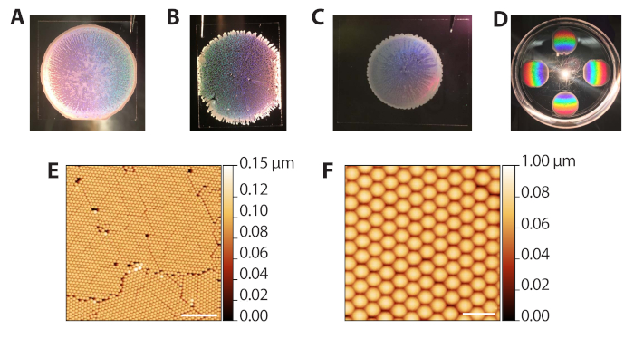
Figure 3: Representative results from evaporative deposition of colloids. (A) Example of optimal colloid deposition. (B) Example of an acceptable colloid deposition in which conditions were more humid (80% RH) than ideal. Holes in the crystal monolayer are apparent. (C) Example of an acceptable colloid deposition in which conditions were drier (65% RH) than optimal. The monolayer regions are slightly translucent while multilayered areas are white and opaque (perimeter and streaks inward). (D) A colloidal crystal illuminated with white light to highlight the rainbow diffraction from the crystals. (E) AFM image (tapping probe AFM in air) of a monolayer of hexagonally packed polystyrene beads from a successful colloid deposition (scale bar = 10 µm). (F) Expanded AFM image of packed beads (scale bar = 2 µm). Please click here to view a larger version of this figure.
to:
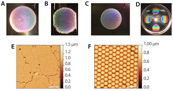
Figure 3: Representative results from evaporative deposition of colloids. (A) Example of optimal colloid deposition. (B) Example of an acceptable colloid deposition in which conditions were more humid (80% RH) than ideal. Holes in the crystal monolayer are apparent. (C) Example of an acceptable colloid deposition in which conditions were drier (65% RH) than optimal. The monolayer regions are slightly translucent while multilayered areas are white and opaque (perimeter and streaks inward). (D) A colloidal crystal illuminated with white light to highlight the rainbow diffraction from the crystals. (E) AFM image (tapping probe AFM in air) of a monolayer of hexagonally packed polystyrene beads from a successful colloid deposition (scale bar = 10 µm). (F) Expanded AFM image of packed beads (scale bar = 2 µm). Please click here to view a larger version of this figure.
프로토콜
An erratum was issued for: Fabrication of Zero Mode Waveguides for High Concentration Single Molecule Microscopy. A figure was updated.
Figure 3 was updated from:
Figure 3: Representative results from evaporative deposition of colloids. (A) Example of optimal colloid deposition. (B) Example of an acceptable colloid deposition in which conditions were more humid (80% RH) than ideal. Holes in the crystal monolayer are apparent. (C) Example of an acceptable colloid deposition in which conditions were drier (65% RH) than optimal. The monolayer regions are slightly translucent while multilayered areas are white and opaque (perimeter and streaks inward). (D) A colloidal crystal illuminated with white light to highlight the rainbow diffraction from the crystals. (E) AFM image (tapping probe AFM in air) of a monolayer of hexagonally packed polystyrene beads from a successful colloid deposition (scale bar = 10 µm). (F) Expanded AFM image of packed beads (scale bar = 2 µm). Please click here to view a larger version of this figure.
to:
Figure 3: Representative results from evaporative deposition of colloids. (A) Example of optimal colloid deposition. (B) Example of an acceptable colloid deposition in which conditions were more humid (80% RH) than ideal. Holes in the crystal monolayer are apparent. (C) Example of an acceptable colloid deposition in which conditions were drier (65% RH) than optimal. The monolayer regions are slightly translucent while multilayered areas are white and opaque (perimeter and streaks inward). (D) A colloidal crystal illuminated with white light to highlight the rainbow diffraction from the crystals. (E) AFM image (tapping probe AFM in air) of a monolayer of hexagonally packed polystyrene beads from a successful colloid deposition (scale bar = 10 µm). (F) Expanded AFM image of packed beads (scale bar = 2 µm). Please click here to view a larger version of this figure.
공개 사항
No conflicts of interest declared.