Waiting
Login processing...

Trial ends in Request Full Access Tell Your Colleague About Jove

Bioengineering

Fabrication of Zero Mode Waveguides for High Concentration Single Molecule Microscopy

Published: May 12, 2020 doi: 10.3791/61154

ERRATUM NOTICE

Summary

Described here is a nanosphere lithography method for parallel fabrication of zero mode waveguides, which are arrays of nanoapertures in a metal-clad glass microscopy coverslip for single molecule imaging at nano- to micromolar concentrations of fluorophores. The method takes advantage of colloidal crystal self-assembly to create a waveguide template.

Abstract

In single molecule fluorescence enzymology, background fluorescence from labeled substrates in solution often limits fluorophore concentration to pico- to nanomolar ranges, several orders of magnitude less than many physiological ligand concentrations. Optical nanostructures called zero mode waveguides (ZMWs), which are 100−200 nm in diameter apertures fabricated in a thin conducting metal such as aluminum or gold, allow imaging of individual molecules at micromolar concentrations of fluorophores by confining visible light excitation to zeptoliter effective volumes. However, the need for expensive and specialized nanofabrication equipment has precluded the widespread use of ZMWs. Typically, nanostructures such as ZMWs are obtained by direct writing using electron beam lithography, which is sequential and slow. Here, colloidal, or nanosphere, lithography is used as an alternative strategy to create nanometer-scale masks for waveguide fabrication. This report describes the approach in detail, with practical considerations for each phase. The method allows thousands of aluminum or gold ZMWs to be made in parallel, with final waveguide diameters and depths of 100−200 nm. Only common lab equipment and a thermal evaporator for metal deposition are required. By making ZMWs more accessible to the biochemical community, this method can facilitate the study of molecular processes at cellular concentrations and rates.

Introduction

Single-molecule techniques such as single molecule fluorescence resonance energy transfer (smFRET) or single molecule fluorescence correlation spectroscopy (FCS) are powerful tools for molecular biophysics, allowing the study of dynamic movements, conformations, and interactions of individual biomolecules in processes such as transcription1,2,3, translation4,5,6, and many others7. For smFRET, total internal reflection fluorescence (TIRF) microscopy is a common method because many tethered molecules may be followed over time, and the evanescent wave generated by TIR is limited to a 100−200 nm region adjacent to the coverslip8. However, even with this restriction on excitation volume, fluorophores of interest still need to be diluted to pM or nM ranges in order to detect single molecule signals above background fluorecence9. Since the Michaelis-Menten constants of cellular enzymes are typically in the μM to mM range10, biochemical reactions in single molecule studies are usually much slower than those in the cell. For example, protein synthesis occurs at 15−20  amino acids per second in E. coli11,12, while most prokaryotic ribosomes in smFRET experiments translate at 0.1−1 amino acid per second13. In protein synthesis, crystal structures and smFRET on stalled ribosomes showed that transfer RNAs (tRNAs) fluctuate between ‘hybrid’ and ‘classical’ states before the tRNA-mRNA translocation step14,15. However, when physiological concentrations of the translocation GTPase factor, EF-G, was present, a different conformation, intermediate between the hybrid and classical states, was observed in smFRET6. Studying dynamic molecular processes at rates and concentrations similar to those in the cell is important, but remains a technical challenge.

A strategy to increase the fluorescent substrate concentration is the use of metal-based, sub-visible wavelength apertures, called zero mode waveguides (ZMWs), to generate confined excitation fields that selectively excite biomolecules localized within the apertures16 (Figure 1). The apertures are typically 100−200 nm in diameter and 100−150 nm in depth17. Above a cutoff wavelength related to the size and shape of the wells (λc ≈ 2.3 times the diameter for circular waveguides with water as the dielectric medium18), no propagating modes are allowed in the waveguide, hence the term zero mode waveguides. However, an oscillating electromagnetic field, termed an evanescent wave, exponentially decaying in intensity still tunnels a short distance into the waveguide18,19. Although similar to TIR evanescent waves, ZMW evanescent waves have a shorter decay constant, resulting in 10−30 nm effective excitation region within the waveguide. At micromolar concentrations of fluorescently labeled ligands, only one or a few molecules are simultaneously present within the excitation region. This restriction of the excitation volume and consequent reduction of background fluorescence enables fluorescence imaging of single molecules at biologically relevant concentrations. This has been applied to many systems20, including FCS measurements of single protein diffusion21, single molecule FRET measurements of low-affinity ligand-protein22 and protein-protein interactions23, and spectro-electrochemical measurements of single molecular turnover events24.

ZMWs have been produced by directly patterning a metal layer using ion beam milling25,26 or electron beam lithography (EBL) followed by plasma-etching16,27. These maskless lithography methods create waveguides in series and typically require access to specialized nanofabrication facilities, preventing widespread adoption of ZMW technology. Another method, ultraviolet nanoimprint lithography lift-off28, uses a quartz slide mold to press an inverse ZMW template onto a resist film like a stamp. While this method is more streamlined, it still requires EBL for fabrication of the quartz mold. This article presents the protocol for a simple and inexpensive templated fabrication method that does not require EBL or ion-beam milling and is based on close-packing of nanospheres to form a lithographic mask.

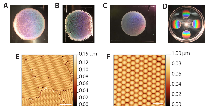
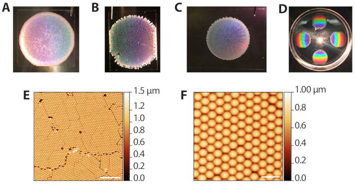
Nanosphere or “natural” lithography, which was first proposed in 1982 by Deckman and Dunsmuir29,30, uses the self-assembly of monodisperse colloidal particles, ranging from tens of nanometers to tens of micrometers31, to create templates for surface patterning via etching and/or deposition of materials. The two-dimensional (2D) or three-dimensional (3D) extended periodic arrays of colloidal particles, referred to as colloidal crystals, are characterized by a bright iridescence from scattering and diffraction32. Although less widely used than electron-beam or photolithography, this masking methodology is simple, low cost, and easily scaled down to create feature sizes below 100 nm.

Directing the self-assembly of colloidal particles determines the success of using colloidal crystals as masks for surface patterning. If the size and shape of particles are homogeneous, colloidal particles can be readily self-assembled with hexagonal packing, driven by entropic depletion33. Water evaporation after drop-coating is an effective route to sediment the colloidal particles, although other methods include dip-coating34, spin coating35, electrophoretic deposition36, and consolidation at an air-water interface37. The protocol presented below is based on the evaporation sedimentation method, which was the simplest to implement. The triangular interstices between close-packed polystyrene beads form openings in which to plate a sacrificial metal, forming posts (Figure 2 and Supplemental Figure 1). Brief annealing of the beads before this step adjusts the shape and diameter of these posts. The beads are removed, a final metal layer is deposited around the posts, and then the posts are removed. After the two metal deposition steps onto the colloidal nanomask, removal of the intermediate posts, and surface chemistry modification for passivation and tethering, ZMW arrays are ready to use for single molecule imaging. More extensive characterization of the ZMW optical properties after fabrication can found in an accompanying article38. Besides a thermal evaporator for vapor deposition of the metals, no specialized tools are required.

Subscription Required. Please recommend JoVE to your librarian.

Protocol

NOTE: All steps can be completed in general lab space.

1. Glass coverslip cleaning

  1. To provide a clean surface for evaporative deposition of colloidal particles, place 24 x 30 mm optical borosilicate glass coverslips (0.16−0.19 mm thickness) within the grooved inserts of a coplin glass staining jar for cleaning.
    NOTE: Make sure the coverslips stand upright and are well-separated so that all surfaces are clearly exposed during the cleaning process.
  2. Pour enough acetone in the staining jar to cover the coverslips, place the cover on, and sonicate for 10 min at 40 °C.
  3. Pour out the acetone and rinse the coverslips by filling the staining jar with distilled H2O and pouring out the water. Repeat 2 more times.
  4. Repeat the acetone sonication (steps 1.2 and 1.3) once more.
  5. Pour enough 200 mM KOH in the jar to cover the coverslips and sonicate, covered, for 20 min at 40 °C.
    NOTE: The KOH slightly etches the glass.
  6. Rinse the coverslips with distilled H2O 6 times.
  7. Add ethanol to cover the coverslips, add the lid, and sonicate for 10 min at 40 °C.
  8. Rinse the coverslips with distilled H2O 3 times.
  9. Pick up each coverslip at the edge using gentle forceps and dry the coverslips with N2 gas. Touch only the edges of the coverslip. Place each of the dried, cleaned coverslips in an individual clean Petri dish.

2. Evaporative deposition of polystyrene beads

  1. To create the colloidal crystal mask for the ZMW array, centrifuge 50 µL of 1 µm diameter, non-functionalized polystyrene beads (2.5% w/v in water) at 15,000 x g, 25 °C for 5 min.
    NOTE: Before pipetting the beads, the stock solution should be briefly vortexed in case the beads have settled to the bottom of the bottle.
  2. Discard the supernatant, leaving as little water remaining as possible.
    NOTE: Residual water can change the evaporation properties of the ethanol resuspension39, so removal of a small amount of beads in order to remove all of the water is acceptable.
  3. Resuspend the beads from step 2.2 in 50 µL of 1:400 TritonX-100:ethanol solvent. Pipette up and down several times to thoroughly mix the beads with the solvent.
    NOTE: TritonX-100:ethanol solvent should be sealed with paraffin film after use and prepared fresh once a month. The beads tend to adhere to the sides of a plastic vessel, such as a microcentrifuge tube, so pipette along the sides to ensure that all beads are resuspended.
  4. To set up a humidity chamber for deposition, place 6 Petri dishes, each with one coverslip, on a bench in a line with lids left slightly ajar. In each dish, move the coverslip to the open region so that the coverslips are exposed to the environment when the humidity is increased in the next step.
  5. Place a hygrometer and a small electric fan centered behind the Petri dishes.
  6. Record the starting relative humidity (RH) in the lab. Fill a 200 mL beaker with 150−200 mL of ~75 °C water and place it behind the fan.
  7. Turn on the fan and cover the Petri dishes, fan, beaker, and hygrometer with an overturned, transparent plastic storage container (66 cm x 46 cm x 38 cm).
  8. Let the RH in the chamber rise to 70−75%, which typically takes 5−10 min.
    NOTE: If the ambient lab RH is low (below ~50%), let the chamber reach a higher RH, but no higher than 80%, to compensate for loss of humidity during deposition (see below).
  9. When the RH reaches 70−75%, record the RH and lift up the plastic storage container slightly to quickly place covers on the Petri dishes, which prevents over-wetting of the coverslips.
    NOTE: The temperature in the chamber will be slightly warmer than room temperature, typically 25−26 °C, as a result of humidification. If moisture is visible on the coverslips, then the glass surfaces are too wet. A commercial glove box might simplify this part of the protocol.
  10. Let the RH in the chamber continue to rise to 85%. At that point, record the RH in the humidity chamber and pipette 5 µL of the bead suspension onto the center of each coverslip.
  11. Close the chamber and Petri dishes after each deposition to minimize loss of humidity. Aim to finish all 6 depositions within 2 min.
  12. Record the RH in the chamber after the deposition.
    NOTE: The RH after deposition will help gauge how fast humidity was lost during deposition, which depends on ambient lab conditions. For a typical successful run, the chamber will start at 85% RH prior to deposition and end at 70−75% RH after the deposition.
  13. Let the bead droplets spread and dry for 5 min.
    NOTE: If the colloidal crystals have many holes or multilayered regions, then the chamber was likely too humid or dry, respectively. Adjust the relative humidity at which to close the Petri dishes and begin the depositions (see the results section for further discussion of optimization).

3. Bead annealing for reducing pore size in the colloidal crystal template

  1. To provide a uniform temperature surface for annealing of the polystyrene beads, which narrows the inter-bead interstices and rounds the interstices’ corners, place a flat, milled aluminum plate on top of a standard ceramic hot plate.
  2. Set the temperature of the hot plate to 107 °C, the glass transition temperature of polystyrene40.
    NOTE: To obtain stable and accurate temperature, a thermocouple probe was held in a 2−3 mm wide and 4−5 mm deep hole in the aluminum plate.
  3. Place a coverslip containing the bead template on the hot aluminum plate and anneal for 20 s (see the discussion section for explanation of melting time).
  4. After heating, remove the coverslip from the aluminum plate and promptly place it on another room temperature aluminum surface to cool it.
    NOTE: It is helpful to either have the coverslips hang slightly over the edge of the plate or mill shallow channels (see the accompanying video) into the plate to facilitate pickup of the coverslips.

4. Nanofabrication of aluminum zero mode waveguides using the colloidal crystal template

  1. Using thermal or electron-beam evaporative deposition, deposit 300 nm of copper at 2 Å/s over the colloidal crystal template to generate posts in the interstices between the beads.
  2. Remove excess metal on top of the beads by gently pressing the surface with tape. Slowly peel the tape to pull off the metal.
    NOTE: Some small patches of reflective excess metal may remain after the tape pull, and these can often be removed by a stream of N2 gas. If substantial patches of reflective excess metal remain after the tape pull, try soaking the templates in toluene for 2 h to partially dissolve the polystyrene beads. Wash the coverslips with distilled water, dry with N2, and repeat the tape pull. The additional soak should not completely dissolve the beads, as the beads help protect the posts from damage during the tape pull.
  3. To dissolve the polystyrene beads, place the bead templates in toluene and soak overnight.
    CAUTION: Toluene fumes may be toxic. Work with toluene under a well-ventilated hood and wear personal protective equipment, including gloves, safety glasses, and a lab coat. Toluene should be stored in ventilated cabinets designated for flammable liquids.
  4. After the toluene incubation, rinse the templates once with chloroform and twice with ethanol. Handle coverslips carefully at this point because the delicate 200−300 nm tall metal posts are now exposed. Dry the templates with N2 and remove residual polymer and contaminants in an oxygen plasma cleaner for 30 min.
    CAUTION: Chloroform fumes may be toxic. Work with chloroform under a well-ventilated hood and wear personal protective equipment, including gloves, safety glasses, and a lab coat. Chloroform should be stored in ventilated cabinets away from other flammable solvents.
  5. Using thermal or electron-beam evaporative deposition, deposit 3 nm of a titanium adhesion layer at 1 Å/s followed by 100−150 nm of aluminum at 4 Å/s around and on top of the copper posts.
    NOTE: One can use thicker cladding to obtain deeper guides and better attenuation of background fluorescence, but this also decreases the yield after exposing and dissolving the posts in the next step (see the discussion section).
  6. To dissolve the metal posts, soak the coverslips in copper etchant (citric acid-based; Table of Materials) for 2 h.
    CAUTION: Metal etchant can cause skin burns. Work with etchants under a well-ventilated hood and wear protective equipment. Wash hands thoroughly after handling. Metal etchant should be stored in ventilated cabinets designated for corrosive liquids.
  7. Rinse the coverslips with distilled water, dry with N2, and gently buff the surface of the metal cladding with lens paper to expose any posts that are still covered in cladding. Place the coverslips back in copper etchant for another 2 h, then rinse again with distilled water and dry with N2.
    NOTE: ZMW slides should be stored in covered, clean Petri dishes to keep them free of contaminants.

5. Nanofabrication of gold zero mode waveguides using the colloidal crystal template

NOTE: The method to fabricate gold ZMWs (Supplemental Figure 1), which mirrors the protocol to fabricate aluminum ZMWs, is provided in this section.

  1. Using thermal or electron beam evaporative deposition, deposit 3 nm of a titanium adhesion layer at 1 Å/s followed by 300 nm of aluminum at 4 Å/s.
  2. Remove excess metal on top of the beads by gently pressing the surface with tape. Slowly peel the tape to pull off the metal.
  3. To dissolve the polystyrene beads, place the bead templates in toluene and soak overnight.
  4. After the toluene incubation, rinse the templates once with chloroform and twice with ethanol. Dry the templates with N2 and remove residual polymer contaminants in an oxygen plasma cleaner for 30 min.
  5. Using thermal or electron beam evaporative deposition, deposit 100−150 nm of gold at 5 Å/s around and on top of the aluminum posts.
  6. To dissolve the metal posts, soak the coverslips in aluminum etchant (phosphoric acid-based; Table of Materials) for 1 h.
  7. Rinse the coverslips with distilled water, dry with N2, and gently buff the surface of the metal cladding with lens paper to expose any posts that are still covered in cladding. Place the coverslips back in aluminum etchant for 1 h, then rinse again with distilled water and dry with N2.
    NOTE: ZMW slides should be stored in covered, clean Petri dishes.

Subscription Required. Please recommend JoVE to your librarian.

Representative Results

The self-assembly of the polystyrene colloidal particles via evaporative sedimentation (steps 2.1−2.13) can produce a range of results since it requires control of the solvent evaporation rate. However, because the depositions are fast (10−15 min per round), the procedure can be quickly optimized for different ambient lab conditions. Figure 3A shows a well-formed colloidal template after deposition and evaporation. Macroscopically, the region of beads is circular, with borders defined by an opaque, multilayered ring of beads. The translucent, but not white regions in the image are the desired monolayer areas. Figure 3B shows a colloidal template that was packed in an overly humid environment (80% RH when Petri dishes were closed). These templates tend not to have a clean circular boundary and have multilayered tendrils extending outward. The deposition is acceptable and can be used in subsequent phases, but the holes in the lattice reduce the number of useable ZMW array areas for single molecule imaging. Figure 3C shows a colloidal template that was packed in an overly dry environment (65% RH when Petri dishes were closed). These templates are usually smaller in diameter compared to the ideal, well spread templates. The deposition can be used, but the multilayered, white regions, which streak inward, reduce the area usable for imaging. Thus, we do not recommend performing more than 6 depositions at a time since depositions toward the end of the process will occur at a lower humidity as the chamber is opened and closed. Figure 3D shows the rainbow pattern produced by diffraction of reflected light from the polystyrene crystal. This pattern can be used to confirm success and quality of crystal packing by eye. Figure 3E,F shows atomic force microscopy (AFM) images of well-packed colloidal templates. The defects between grains arise from jamming during the evaporative sedimentation41, and distinct grains can be seen with a 10x objective. Thus, examining the colloid depositions with a low-power light microscope can also be used to assess packing.

After deposition of copper onto the annealed colloidal templates (step 4.1), the rainbow diffraction pattern should still be visible and enhanced by the reflective metal coating the tops of the beads (Figure 4A,B). The templates lose the reflective rainbow diffraction pattern after the Scotch tape pull (step 4.2) that removes excess copper (Figure 4C). Figure 4D,E shows AFM images of a typical field of copper posts after metal deposition. The defects in between the colloidal crystal grains in Figure 3E are visible in the copper post images as larger regions of copper. Analysis of AFM images shows that, for a copper deposition thickness of 300 nm, the eventual copper posts average 255 nm (Figure 4F) in height and 121 nm in diameter (Figure 4G).

Deposition of the aluminum cladding (step 4.5) where the beads were and on top of the copper posts, and subsequent dissolution of the posts (steps 4.6 and 4.7) result in the aluminum ZMWs shown in Figure 5A−C. Defects between the colloidal crystal grains are visible as larger openings (Figure 5B). The average distance between the ZMW centers in Figure 5C is 559 nm, consistent with the spacing set by the hexagonal close packing geometry of the 1 µm beads (Equation 1 Using polystyrene templates that were annealed for 20 s results in waveguides that are on average 118 nm in diameter (Figure 5D,E), consistent with the post diameters and sufficiently small to cut off propagation of visible light. A height profile of a waveguide from Figure 5D also shows that it is ~120 nm deep.

Single molecule FRET was performed in the ZMWs to test for functionality (Figure 6A). A typical field of ZMWs for imaging is shown in Figure 6B, which contains >3000 waveguides in a 40 x 80 µm field of view. The ZMWs were first passivated using protocols described previously42,43. Briefly, the aluminum ZMWs were passivated with poly(vinylphosphonic acid) to coat the aluminum cladding followed by methoxy-terminated polyethylene glycol (PEG) doped with biotin-terminated PEG to coat the glass bottoms of the ZMWs. Gold ZMWs can be passivated with thiol-derivatized PEG to coat the gold cladding followed by a similar PEG treatment for the glass bottoms. Flow chambers, ~20 µL volume, were then constructed for single molecule imaging44. Single molecule FRET imaging of the DNA duplexes was performed as described previously38. Briefly, 100 pM−1 nM of cyanine-3/cyanine-5 (Cy3/Cy5), biotinylated DNA duplexes (33 base pair length) were incubated for 10 min in flow channels functionalized with streptavidin (5 min incubation, 0.5 mg/mL solution). The concentration of labeled macromolecules can be titrated to achieve ~20% loading of the waveguides with one molecule, leading to <5% waveguides loaded with more than one molecule, based on Poisson distributed loading (most waveguides, ~75%, will have no molecules)45. Unbound DNA was washed away with nuclease-free duplex buffer followed by illumination buffer (0.3% [w/v] glucose, 300 μg/mL glucose oxidase, 120 μg/mL catalase, and 1.5 mM Trolox [6-hydroxy-2,5,7,8-tetramethyl-chromane-2-carboxylic acid]). Non-biotinylated Cy5-labeled DNA duplexes (33 base pair length) were present in the illumination buffer at 0, 50, 100, and 500 nM as background fluorophores in solution. Single molecule FRET traces from the immobilized Cy3/Cy5 duplex DNA molecules were recorded with a custom-built TIRF microscope adjusted to epi-fluorescence conditions. Movies were recorded with a 1.48 numerical aperture (NA) 100x oil immersion objective with alternating 532 nm and 640 nm excitation (100 ms exposure) and a dual view spectral splitter to record Cy3 and Cy5 emission simultaneously on an electron-multiplying charge-coupled device (EMCCD) camera. Single molecule FRET traces with single step bleaches in the Cy5 channel were detectable at all concentrations of ambient Cy5 tested (Figure 6C−F). In comparison, single molecules would only be detectable in TIRF illumination with pM to low nM solution fluorophore concentrations46.

Figure 1
Figure 1: Schematic of zero mode waveguides. Diagram of ZMW array with expanded cross-sectional diagram of a single ZMW on the right. Single fluorescently tagged enzymes of interest (brown ribosome with red circle to represent fluorescent dye) chemically immobilized (via the mRNA in this example) to the glass bottom of the ZMWs (typically functionalized with biotinylated-PEG) can be imaged with a typical laser-based epifluorescence microscopy setup. The 532 nm excitation light (green arrows) is reflected at the glass-metal boundary due to the small size of the aperture (100−200 nm diameter), but a non-propagating evanescent wave that decays exponentially in intensity is present within the ZMW. This results in a 10−30 nm effective illumination depth (green shading in aperture). Individual fluorescent ligands (blue tRNAs with green circles as fluorescent tags) at nM to µM concentrations are added. An individual ligand that diffuses into the aperture and interacts with the enzyme is imaged without prohibitive background fluorescence. Please click here to view a larger version of this figure.

Figure 2
Figure 2: Schematic of colloidal templating method developed to fabricate aluminum ZMW arrays. Polystyrene beads, 1 µm in diameter, are deposited and self-assembled on a cleaned glass coverslip, as described in section 2 of the protocol. Beads are then annealed to reduce pore sizes (section 3), followed by copper deposition and bead dissolution in toluene. Aluminum is deposited around and on top of the copper posts, which are then selectively etched away to leave behind a hexagonal array of nanoapertures (section 4). For the last three steps, cross-sectional views are provided to the right of the plan views to show the widths and heights of the copper posts and aluminum ZMWs. Please click here to view a larger version of this figure.

Figure 3
Figure 3: Representative results from evaporative deposition of colloids. (A) Example of optimal colloid deposition. (B) Example of an acceptable colloid deposition in which conditions were more humid (80% RH) than ideal. Holes in the crystal monolayer are apparent. (C) Example of an acceptable colloid deposition in which conditions were drier (65% RH) than optimal. The monolayer regions are slightly translucent while multilayered areas are white and opaque (perimeter and streaks inward). (D) A colloidal crystal illuminated with white light to highlight the rainbow diffraction from the crystals. (E) AFM image (tapping probe AFM in air) of a monolayer of hexagonally packed polystyrene beads from a successful colloid deposition (scale bar = 10 µm). (F) Expanded AFM image of packed beads (scale bar = 2 µm). Please click here to view a larger version of this figure.

Figure 4
Figure 4: Macroscopic and microscopic images of ZMW templates after copper deposition. (A) Picture of slides after physical evaporation of copper on top of the bead templates. (B) Rainbow diffraction pattern from bead templates after copper deposition. (C) Picture of a template (right) after a tape pull to remove excess copper and the tape (left). (D) AFM image of copper posts after tape pull and complete dissolution of the polystyrene beads (scale bar = 5 µm). (E) Higher magnification AFM image of panel D (scale bar = 2 µm). (F) Histogram of the copper post heights (defined as maximum height measurement within each post), n = 534. (G) Histogram of the copper post Feret diameters, n = 201. Feret diameter is the maximum distance between two parallel lines tangent to the post boundary (quantified in ImageJ47). To identify particles for analysis, a threshold halfway between the top of the cladding and the bottom glass surface was used. Please click here to view a larger version of this figure.

Figure 5
Figure 5: Macroscopic and microscopic images of aluminum ZMWs. (A) Picture of slides after physical evaporative deposition of 150 nm of aluminum around and on top of the copper posts. (B) AFM image of aluminum ZMWs after post dissolution (scale bar = 5 µm). (C) Higher magnification image of panel B (scale bar = 0.2 µm). (D) Typical depth profile of an individual ZMW from panel C. Profile taken from the green line drawn in panel C. (E) Histogram of ZMW Feret diameters, n = 240. Feret diameters were measured as in Figure 4. Please click here to view a larger version of this figure.

Figure 6
Figure 6: Single molecule FRET imaging in ZMWs. (A) Schematic (not to scale) of single molecule FRET imaging of Cy3, Cy5-labeled DNA duplexes in ZMWs with Cy5 labeled duplexes in the background. (B) Example field of ZMWs under white light illumination (scale bar = 10 µm). (C−F) Single molecule FRET recordings of DNA duplexes immobilized in the ZMWs in the presence of 0 (C), 50 (D), 100 (E), and 500 nM (F) Cy5-labeled duplexes in solution. For each concentration, the top panel shows the Cy3 (green) and Cy5 (red) fluorescence intensity under 532 nm laser illumination (FRET imaging), middle panel shows the Cy5 fluorescence intensity under 640 nm laser illumination (direct acceptor excitation), and the lowest panel shows the FRET efficiency (Equation 2 ) calculated from the raw Cy3 (ID) and Cy5 (IA) fluorescence intensities. During imaging, the excitation wavelength alternated between 532 and 640 nm every 100 ms. Please click here to view a larger version of this figure.

Supplemental Figure 1: Schematic of colloidal templating method developed to fabricate gold ZMW array. Protocol to fabricate gold ZMW array is analogous to protocol to fabricate aluminum ZMW array (Figure 2). Instead of depositing copper on top of the polystyrene beads, aluminum is deposited. After dissolving the beads in toluene, gold is deposited instead of aluminum on top of the posts. Aluminum posts are then selectively etched to leave behind gold ZMW array. For the last three steps, cross-sectional views are provided to the right of the plan views to show the widths and heights of the aluminum posts and gold ZMWs. Please click here to download this file.

Supplemental Figure 2: Finite element modeling of electromagnetic field propagation in ZMWs. (A−D) Cross sections of the magnitude of the time-averaged Poynting vector (W/m2) through a waveguide made from an unannealed template (A,C) and an annealed template (B,D). Linearly polarized electromagnetic plane waves (1 W distributed over the area of the slide) at the wavelengths listed in the figure (400 nm or 1,000 nm) were projected onto the bottom surface, and the lowest (fundamental) mode, which has the lowest wavenumber, was computed using modeling software (Table of Materials) with the finite element method for solving Maxwell’s equations and appropriate boundary conditions. The boundaries of the waveguides were assumed to be perfect electrical conductors, which is well approximated by aluminum or gold walls. The cross-section from the unannealed waveguide template was determined by the hexagonal packing of 1 μm diameter circles, and the three-pointed tips from the resulting triangular shape were clipped to ~60 nm width to model a realistic physical aperture. The cross-section from the annealed templates was approximated as a circle 130 nm in diameter. Both waveguides had a 130 nm depth, similar to the cladding depth after fabrication. (E,F) In addition to excitation wavelengths of 400 nm and 1,000 nm, the models were solved at 100 excitation wavelengths evenly spaced between 400 nm and 1,000 nm, and the effective mode index (defined as Equation 3, where kz is the wavenumber in the waveguide, which is decreased due to restriction in the transverse plane, and k is the excitation light wavenumber in vacuum) was plotted against excitation wavelength for the triangular (E) and circular (F) waveguides. For shorter wavelengths, higher modes are excited, and the effective mode index increases (max effective mode index is 1, which is the limiting case where the electromagnetic plane wave travels unbounded in the transverse dimension). The effective cutoff wavelengths of the waveguides were estimated as the wavelength at which the effective mode index drops to 0. Note that the circular guide λcutoff = 221 nm from finite element modelling (F) is consistent with the theoretical prediction of a circular waveguide’s cutoff wavelength (λcutoff,analytical = 1.7d = 221 nm, where d is the waveguide diameter). Please click here to download this file.

Supplemental Figure 3: Representative results from Au ZMW fabrication. (A) Macroscopic picture of gold ZMW arrays. (B−D) AFM images of aluminum posts from a bead template that was not annealed (B), a template that was annealed at 107 °C for 20 s (C), and a template that was annealed at 107 °C for 25 s (D). (E) AFM image of gold ZMWs after dissolution of aluminum posts. (F) Higher magnification AFM image of panel E. (G) Typical depth profile of a gold ZMW. Profile taken from the green line drawn in panel F (scale bar = 1 µm in B, C, D, and F; 5 µm in E). Please click here to download this file.

Subscription Required. Please recommend JoVE to your librarian.

Discussion

For the colloidal self-assembly (protocol section 2), the use of ethanol rather than water as the suspension solvent speeds the evaporation process so that templates are ready in 2−3 min after deposition rather than 1−2 h as in previous methods48,49. The evaporative sedimentation protocol presented here is also simpler than previous sedimentation protocols that require controlling surface tilt, temperature, and air volume above the suspension49,50,51. The particle volume fraction used in this protocol is 2.4%, higher than the 0.2−0.5% used in previous sedimentation methods48, which resuspended colloids in water-glycerol mixtures for much longer settling time-scales. However, the quality of the depositions is robust to changes in the particle volume fraction, with past studies finding that it can be varied between 2−10%49,50,51. The grain sizes of the colloidal crystals obtained in a successful deposition from this protocol are 20−30 µm across, larger than grains from previous sedimentation methods (typically several hundred nanometers across)48,49. Macroscopically, the roughly 2 cm in diameter areas of colloidal monolayer are also comparable to the 1 cm areas produced by previous methods49. The large size of the colloidal crystal templates produced in this method also allows 3−5 separated flow chambers44, each about 3−4 mm wide, to be made on each ZMW slide. Thus, multiple independent single molecule experiments can be performed on each slide.

Annealing the colloidal bead templates (protocol section 3) after self-assembly is a simple, but crucial step for sufficiently reducing background fluorescence with the ZMWs. As Supplemental Figure 2 shows, the effective cutoff wavelength for a waveguide with the triangular cross-section from an unannealed template is 894 nm. In comparison, the effective cutoff wavelength for a 130 nm diameter circular waveguide from an annealed template is 221 nm, as determined both analytically (1.7 times the diameter of the guide18) and numerically. Using smaller beads for deposition could also reduce the size of the template pores, but the waveguides would then be spaced closer than 200 nm, which is around the diffraction limit of visible light. Furthermore, the waveguides would remain triangular in cross-section, which leads to nonsymmetric power propagation through the waveguide (Supplemental Figure 2A−D). One drawback of the annealing step is that variability in melting time can introduce fluctuations in waveguide diameter, so accurate timing helps to minimize variation between batches. The interstices start to close at annealing times longer than 25 s, and post diameters do not decrease very much between 20−25 s (Supplemental Figure 3B−D). A quick test for interstice closure is to check whether annealed templates still produce a rainbow diffraction pattern when illuminated with light and viewed at an angle. If not, the majority of interstices likely have closed. The relationship between annealing time and typical pore diameters has been presented earlier38.

After achieving the desired pore size during the annealing step, copper is deposited (step 4.1) onto the templates to create a shadow of the mask. It is important to use line of sight deposition, with the metal approaching the template as perpendicularly as possible. Thus, increasing the distance between the sample and metal source as well as ensuring the plate holding the templates is not spinning, as is automatically done in some vapor deposition machines, will aid in minimizing lateral deposition of metal onto the polystyrene substrate. However, some lateral deposition is inevitable, which reduces the size of the interstitial hole and thus the post cross-section as more metal is deposited52. This results in pyramidal metal posts rather than prism-like structures52.

Because the copper posts are likely pyramidal rather than prism shaped, aluminum deposition (step 4.5) on top of the posts also covers some of the sloped sides, blocking accessibility of the copper etchant for some of the posts. Thus, the lens paper buffing step (step 4.7 or 5.7) was added after the first soak in etchant to mechanically disrupt any copper posts still covered in aluminum. Depositing more copper to create taller posts also makes the posts more susceptible to mechanical disruption during the lens paper buffing. However, more than 500 nm of copper should not be deposited since the goal of deposition is to project the interstitial hole at the 500 nm midline of the 1 µm beads.

Another potential difficulty is the unintended removal of aluminum cladding during the lens paper buffing (step 4.7 or 5.7). It was found that loss of aluminum cladding during buffing became more frequent after the annealing step was added, likely due to increased polystyrene residue, which can interfere with aluminum adherence to glass (protocol section 3). However, the overnight toluene soak (step 4.3 or 5.3) after the tape pull resolved this issue. In the AFM image in Figure 4E, some residual rings of polystyrene can be seen between the posts, but the aluminum cladding still resisted multiple buffs in step 4.7. If loss of the aluminum cladding remains an issue after the overnight toluene soak, an RCA-1 (standard clean-1) wash, piranha wash, or further oxygen plasma cleaning can be added to step 4.4 or 5.4. These wash steps can also be added after the final etch step (step 4.7 or 5.7) and before passivation in order to further clean the ZMWs.

The performance of the ZMWs in single molecule FRET experiments was similar to that of ZMWs fabricated with EBL. In a previous study53 performing single molecule FRET on Cy3 labeled single stranded DNA with Cy5 labeled DNA helicase loader protein in solution (the same donor-acceptor arrangement as that in Figure 6A), FRET events were clearly discernible at 100 nM Cy5 background, were less clear (lower acceptor trace signal to noise) at 1 µM, and not discernible at 10 µM. We note that a previous study with commercial ZMWs reported single molecule FRET acceptor signals at background concentrations as high as 1 mM54, higher than we and other previous studies42,53 with in-house fabricated ZMWs have achieved. Further discussion of the signal-to-background performance among ZMWs is given in Jamiolkowski et al.38. Nonspecific interaction of fluorescent sample with the ZMW surfaces53 is a common challenge limiting access to higher concentrations, especially if the diffusing fluorescent species in solution is a large macromolecule. Studies with ZMWs on complex biochemical systems such as translation have typically limited free fluorescent substrate concentrations to 100−250 nM55,56,57,58. Regardless of the intended application of the ZMWs, optimization of passivation methods for different systems will likely be necessary to maintain acceptable signal to noise at high concentrations.

Overall, the method presented here requires no specialized skills or equipment, allows parallel fabrication of many templates at once, and can be adapted to fabricate ZMWs in different metals. In this work, copper and aluminum were substituted with aluminum and gold, respectively, to fabricate gold ZMWs (Supplemental Figure 3). This is advantageous for labs that use passivation methods of gold rather than aluminum. In addition, gold ZMWs have been shown to enhance emission for fluorophores that absorb in the red region of the visible spectrum, while aluminum ZMWs enhance emission for fluorophores that absorb in the green region59. In the future, fluorescent signal intensity from ZMWs fabricated with this method might be enhanced by etching into the glass below the ZMW metal cladding using HF16,26,60. This brings the immobilized biomolecules farther away from the metal walls, which can quench fluorophores61. Furthermore, there is a maximum in excitation illumination intensity below the entrance of the aperture, and this has been exploited previously to enhance single molecule emission26,60.

Subscription Required. Please recommend JoVE to your librarian.

Disclosures

The authors have nothing to disclose.

Acknowledgments

This work was supported by NIH grants R01GM080376, R35GM118139, and NSF Center for Engineering MechanoBiology CMMI: 15-48571 to Y.E.G., and by an NIAID pre-doctoral NRSA fellowship F30AI114187 to R.M.J.

Materials

Name Company Catalog Number Comments
1. Glass Coverslip Cleaning
Acetone Sigma 32201 1 L
Coplin glass staining jar Fisher Scientific 08-817 Staining jar with 8 grooves and molded glass cover
Coverslips VWR 48404-467 24 mm x 30 mm (No.1½, Rectangular)
Ethanol Sigma E7023 1 L
KOH Sigma 30603 Potassium hydroxide
Petri dishes Fisher Scientific R80115TS 100 mm diameter, 15 mm deep
Sonicator Branson Z245143 Tabletop ultrasonic cleaner, 5510
2. Evaporative Deposition of Polystyrene Beads
Clear storage container Fisher Scientific 50-110-8222 26 x 18 x 15 in.
Desk fan O2Cool FD05001A Any small desk (~5 in.) fan will work
Glass beaker Fisher Scientific 02-555-25B 250 mL
Humidity meter Fisher Scientific 11-661-19
Microcentrifuge tubes Fisher Scientific 21-402-903 1.5 mL
Polystyrene microspheres Polysciences 18602-15 1.00 µm diameter, non-functionalized
Triton X-100 deturgent Sigma X100 100 mL
3. Bead Annealing for Reducing Pore Size in the Colloidal Crystal Template
Aluminum plate Fisher Scientific AA11062RY Customized in-house to 14 cm x 14 cm
Ceramic hotplate Fisher Scientific HP88857100 13 x 8.2 x 3.8 in.
Temperature controller McMaster-Carr 38615K71 Read temperature with thermocouple probe
Thermocouple probe McMaster-Carr 9251T93 Type K, surface probe
4/5. Nanofabrication of Zero Mode Waveguides Using the Colloidal Crystal Template
Aluminum etchant Transene Type A
Aluminum pellets Kurt J. Lesker EVMAL40QXHB For electron beam evaporation
Chloroform Sigma 288306 1 L
Copper etchant Transene 49-1
Copper pellets Kurt J. Lesker EVMCU40QXQA For electron beam evaporation
Gold pellets Kurt J. Lesker EVMAUXX40G For electron beam evaporation
Lens paper Thorlabs MC-5
Plasma cleaner Harrick Plasma PDC-32G
Scotch tape Staples MMM119
Thin film deposition system Kurt J. Lesker PVD-75 Tabletop thermal evaporation system will also work
Titanium pellets Kurt J. Lesker EVMTI45QXQA For electron beam evaporation
Toluene Sigma 244511 1 L
Representative Results
COMSOL Multiphysics Modeling Software COMSOL, Inc.
Dual View spectral splitter Photometrics, Inc.

DOWNLOAD MATERIALS LIST

References

  1. Kapanidis, A. N., et al. Initial transcription by RNA polymerase proceeds through a DNA-scrunching mechanism. Science. 314 (5802), 1144-1147 (2006).
  2. Santoso, Y., et al. Conformational transitions in DNA polymerase I revealed by single-molecule FRET. Proceedings of the National Academy of Sciences of the United States of America. 107 (2), 715-720 (2010).
  3. Herbert, K. M., Greenleaf, W. J., Block, S. M. Single-molecule studies of RNA polymerase: motoring along. Annual Review of Biochemistry. 77, 149-176 (2008).
  4. Chen, C., et al. Dynamics of translation by single ribosomes through mRNA secondary structures. Nature Structural & Molecular Biology. 20 (5), 582-588 (2013).
  5. Chen, C., et al. Single-molecule fluorescence measurements of ribosomal translocation dynamics. Molecular Cell. 42 (3), 367-377 (2011).
  6. Jamiolkowski, R. M., Chen, C., Cooperman, B. S., Goldman, Y. E. tRNA Fluctuations Observed on Stalled Ribosomes Are Suppressed during Ongoing Protein Synthesis. Biophysical Journal. 113 (11), 2326-2335 (2017).
  7. Myong, S., Stevens, B. C., Ha, T. Bridging Conformational Dynamics and Function Using Single-Molecule Spectroscopy. Structure. 14 (4), 633-643 (2006).
  8. Martin-Fernandez, M. L., Tynan, C. J., Webb, S. E. A 'pocket guide' to total internal reflection fluorescence. Journal of Microscopy. 252 (1), 16-22 (2013).
  9. Holzmeister, P., Acuna, G. P., Grohmann, D., Tinnefeld, P. Breaking the concentration limit of optical single-molecule detection. Chemical Society Reviews. 43 (4), 1014-1028 (2014).
  10. Scheer, M., et al. BRENDA, the enzyme information system in 2011. Nucleic Acids Research. 39, 670-676 (2011).
  11. Kudva, R., et al. Protein translocation across the inner membrane of Gram-negative bacteria: the Sec and Tat dependent protein transport pathways. Research in Microbiology. 164 (6), 505-534 (2013).
  12. Talkad, V., Schneider, E., Kennell, D. Evidence for variable rates of ribosome movement in Escherichia coli. Journal of Molecular Biology. 104 (1), 299-303 (1976).
  13. Blanchard, S. C., Kim, H. D., Gonzalez, R. L., Puglisi, J. D., Chu, S. tRNA dynamics on the ribosome during translation. Proceedings of the National Academy of Sciences of the United States of America. 101 (35), 12893-12898 (2004).
  14. Dunkle, J. A., et al. Structures of the bacterial ribosome in classical and hybrid states of tRNA binding. Science. 332 (6032), 981-984 (2011).
  15. Kim, H. D., Puglisi, J. D., Chu, S. Fluctuations of transfer RNAs between classical and hybrid states. Biophysical Journal. 93 (10), 3575-3582 (2007).
  16. Levene, M. J., et al. Zero-mode waveguides for single-molecule analysis at high concentrations. Science. 299 (5607), 682-686 (2003).
  17. Zhu, P., Craighead, H. G. Zero-mode waveguides for single-molecule analysis. Annual Review of Biophysics. 41, 269-293 (2012).
  18. Pollack, G. L., Stump, D. R. Electromagnetism. , Addison-Wesley. Boston, MA. (2002).
  19. Jackson, J. D. Classical electrodynamics. Third edition. , Wiley. New York, NY. (1999).
  20. Crouch, G. M., Han, D., Bohn, P. W. Zero-mode waveguide nanophotonic structures for single molecule characterization. Journal of Physics D: Applied Physics. 51 (19), 193001 (2018).
  21. Wenger, J., et al. Dual-color fluorescence cross-correlation spectroscopy in a single nanoaperture: towards rapid multicomponent screening at high concentrations. Optics Express. 14 (25), 12206-12216 (2006).
  22. Goldschen-Ohm, M. P., et al. Structure and dynamics underlying elementary ligand binding events in human pacemaking channels. eLife. 5, 20797 (2016).
  23. Miyake, T., et al. Real-Time Imaging of Single-Molecule Fluorescence with a Zero-Mode Waveguide for the Analysis of Protein-Protein Interaction. Analytical Chemistry. 80 (15), 6018-6022 (2008).
  24. Zhao, J., Branagan, S. P., Bohn, P. W. Single-Molecule Enzyme Dynamics of Monomeric Sarcosine Oxidase in a Gold-Based Zero-Mode Waveguide. Applied Spectroscopy. 66 (2), 163-169 (2012).
  25. Fore, S., Yuen, Y., Hesselink, L., Huser, T. Pulsed-interleaved excitation FRET measurements on single duplex DNA molecules inside C-shaped nanoapertures. Nano Letters. 7 (6), 1749-1756 (2007).
  26. Rigneault, H., et al. Enhancement of single-molecule fluorescence detection in subwavelength apertures. Physical Review Letters. 95 (11), 117401 (2005).
  27. Foquet, M., et al. Improved fabrication of zero-mode waveguides for single-molecule detection. Journal of Applied Physics. 103 (3), 034301 (2008).
  28. Wada, J., et al. Fabrication of Zero-Mode Waveguide by Ultraviolet Nanoimprint Lithography Lift-Off Process. Japanese Journal of Applied Physics. 50 (6), 06 (2011).
  29. Fischer, U. C., Zingsheim, H. P. Submicroscopic pattern replication with visible light. Journal of Vacuum Science and Technology. 19 (4), 881-885 (1981).
  30. Deckman, H. W., Dunsmuir, J. H. Natural lithography. Applied Physics Letters. 41 (4), 377-379 (1982).
  31. Li, B., Zhou, D., Han, Y. Assembly and phase transitions of colloidal crystals. Nature Reviews Materials. 1 (2), 15011 (2016).
  32. Bohn, J. J., Tikhonov, A., Asher, S. A. Colloidal crystal growth monitored by Bragg diffraction interference fringes. Journal of Colloid and Interface Science. 350 (2), 381-386 (2010).
  33. Dimitrov, A. S., Nagayama, K. Continuous Convective Assembling of Fine Particles into Two-Dimensional Arrays on Solid Surfaces. Langmuir. 12 (5), 1303-1311 (1996).
  34. Pisco, M., et al. Nanosphere lithography for optical fiber tip nanoprobes. Light: Science & Applications. 6 (5), 16229 (2017).
  35. Chandramohan, A., et al. Model for large-area monolayer coverage of polystyrene nanospheres by spin coating. Scientific Reports. 7, 40888 (2017).
  36. Besra, L., Liu, M. A review on fundamentals and applications of electrophoretic deposition (EPD). Progress in Materials Science. 52 (1), 1-61 (2007).
  37. Yu, J., et al. Preparation of High-Quality Colloidal Mask for Nanosphere Lithography by a Combination of Air/Water Interface Self-Assembly and Solvent Vapor Annealing. Langmuir. 28 (34), 12681-12689 (2012).
  38. Jamiolkowski, R. M., et al. Nanoaperture fabrication via colloidal lithography for single molecule fluorescence analysis. PLoS ONE. 14 (10), 0222964 (2019).
  39. Innocenzi, P., et al. Evaporation of Ethanol and Ethanol-Water Mixtures Studied by Time-Resolved Infrared Spectroscopy. The Journal of Physical Chemistry A. 112 (29), 6512-6516 (2008).
  40. Rieger, J. The glass transition temperature of polystyrene. Journal of Thermal Analysis. 46 (3), 965-972 (1996).
  41. Donev, A., Torquato, S., Stillinger, F. H., Connelly, R. Jamming in hard sphere and disk packings. Journal of Applied Physics. 95 (3), 989-999 (2004).
  42. Kinz-Thompson, C. D., et al. Robustly Passivated, Gold Nanoaperture Arrays for Single-Molecule Fluorescence Microscopy. ACS Nano. 7 (9), 8158-8166 (2013).
  43. Korlach, J., et al. Selective aluminum passivation for targeted immobilization of single DNA polymerase molecules in zero-mode waveguide nanostructures. Proceedings of the National Academy of Sciences of the United States of America. 105 (4), 1176-1181 (2008).
  44. Chandradoss, S. D., et al. Surface passivation for single-molecule protein studies. Journal of Visualized Experiments. (86), e50549 (2014).
  45. Plénat, T., Yoshizawa, S., Fourmy, D. DNA-Guided Delivery of Single Molecules into Zero-Mode Waveguides. ACS Applied Materials & Interfaces. 9 (36), 30561-30566 (2017).
  46. Kudalkar, E. M., Davis, T. N., Asbury, C. L. Single-Molecule Total Internal Reflection Fluorescence Microscopy. Cold Spring Harbor protocols. 2016 (5), 077800 (2016).
  47. Schindelin, J., et al. Fiji: an open-source platform for biological-image analysis. Nature Methods. 9 (7), 676-682 (2012).
  48. Hoogenboom, J. P., Derks, D., Vergeer, P., Blaaderen, A. v Stacking faults in colloidal crystals grown by sedimentation. The Journal of Chemical Physics. 117 (24), 11320-11328 (2002).
  49. Micheletto, R., Fukuda, H., Ohtsu, M. A Simple Method for the Production of a Two-Dimensional, Ordered Array of Small Latex Particles. Langmuir. 11 (9), 3333-3336 (1995).
  50. Denkov, N., et al. Mechanism of formation of two-dimensional crystals from latex particles on substrates. Langmuir. 8 (12), 3183-3190 (1992).
  51. Okubo, T. Convectional, sedimentation and drying dissipative patterns of colloidal crystals of poly(methyl methacrylate) spheres on a watch glass. Colloid and Polymer Science. 286 (11), 1307-1315 (2008).
  52. Ye, S., Routzahn, A. L., Carroll, R. L. Fabrication of 3D Metal Dot Arrays by Geometrically Structured Dynamic Shadowing Lithography. Langmuir. 27 (22), 13806-13812 (2011).
  53. Zhao, Y., et al. Dark-Field Illumination on Zero-Mode Waveguide/Microfluidic Hybrid Chip Reveals T4 Replisomal Protein Interactions. Nano Letters. 14 (4), 1952-1960 (2014).
  54. Goldschen-Ohm, M. P., White, D. S., Klenchin, V. A., Chanda, B., Goldsmith, R. H. Observing Single-Molecule Dynamics at Millimolar Concentrations. Angewandte Chemie International Edition. 56 (9), 2399-2402 (2017).
  55. Noriega, T. R., Chen, J., Walter, P., Puglisi, J. D. Real-time observation of signal recognition particle binding to actively translating ribosomes. eLife. 3, 04418 (2014).
  56. Uemura, S., et al. Real-time tRNA transit on single translating ribosomes at codon resolution. Nature. 464 (7291), 1012-1017 (2010).
  57. Choi, J., Puglisi, J. D. Three tRNAs on the ribosome slow translation elongation. Proceedings of the National Academy of Sciences of the United States of America. 114 (52), 13691-13696 (2017).
  58. Eid, J., et al. Real-Time DNA Sequencing from Single Polymerase Molecules. Science. 323 (5910), 133-138 (2009).
  59. Martin, W. E., Srijanto, B. R., Collier, C. P., Vosch, T., Richards, C. I. A Comparison of Single-Molecule Emission in Aluminum and Gold Zero-Mode Waveguides. The Journal of Physical Chemistry A. 120 (34), 6719-6727 (2016).
  60. Wenger, J., et al. Single molecule fluorescence in rectangular nano-apertures. Optics Express. 13 (18), 7035-7044 (2005).
  61. Pineda, A. C., Ronis, D. Fluorescence quenching in molecules near rough metal surfaces. The Journal of Chemical Physics. 83 (10), 5330-5337 (1985).

Tags

Zero Mode Waveguides Single Molecule Microscopy Nanosphere Lithography Fabrication Low Cost Method Fluorescent Reagents Evaporative Deposition Colloidal Particles Borosilicate Glass Coverslips Coplin Glass Staining Jar Acetone Potassium Hydroxide Ethanol Forceps Petri Dish Centrifuge Polystyrene Beads

Erratum

Formal Correction: Erratum: Fabrication of Zero Mode Waveguides for High Concentration Single Molecule Microscopy
Posted by JoVE Editors on 08/10/2021. Citeable Link.

An erratum was issued for: Fabrication of Zero Mode Waveguides for High Concentration Single Molecule Microscopy. A figure was updated.

Figure 3 was updated from:

Figure 3
Figure 3: Representative results from evaporative deposition of colloids. (A) Example of optimal colloid deposition. (B) Example of an acceptable colloid deposition in which conditions were more humid (80% RH) than ideal. Holes in the crystal monolayer are apparent. (C) Example of an acceptable colloid deposition in which conditions were drier (65% RH) than optimal. The monolayer regions are slightly translucent while multilayered areas are white and opaque (perimeter and streaks inward). (D) A colloidal crystal illuminated with white light to highlight the rainbow diffraction from the crystals. (E) AFM image (tapping probe AFM in air) of a monolayer of hexagonally packed polystyrene beads from a successful colloid deposition (scale bar = 10 µm). (F) Expanded AFM image of packed beads (scale bar = 2 µm). Please click here to view a larger version of this figure.

to:

Figure 3
Figure 3: Representative results from evaporative deposition of colloids. (A) Example of optimal colloid deposition. (B) Example of an acceptable colloid deposition in which conditions were more humid (80% RH) than ideal. Holes in the crystal monolayer are apparent. (C) Example of an acceptable colloid deposition in which conditions were drier (65% RH) than optimal. The monolayer regions are slightly translucent while multilayered areas are white and opaque (perimeter and streaks inward). (D) A colloidal crystal illuminated with white light to highlight the rainbow diffraction from the crystals. (E) AFM image (tapping probe AFM in air) of a monolayer of hexagonally packed polystyrene beads from a successful colloid deposition (scale bar = 10 µm). (F) Expanded AFM image of packed beads (scale bar = 2 µm). Please click here to view a larger version of this figure.

Fabrication of Zero Mode Waveguides for High Concentration Single Molecule Microscopy
Play Video
PDF DOI DOWNLOAD MATERIALS LIST

Cite this Article

Chen, K. Y., Jamiolkowski, R. M.,More

Chen, K. Y., Jamiolkowski, R. M., Tate, A. M., Fiorenza, S. A., Pfeil, S. H., Goldman, Y. E. Fabrication of Zero Mode Waveguides for High Concentration Single Molecule Microscopy. J. Vis. Exp. (159), e61154, doi:10.3791/61154 (2020).

Less
Copy Citation Download Citation Reprints and Permissions
View Video

Get cutting-edge science videos from JoVE sent straight to your inbox every month.

Waiting X
Simple Hit Counter