We report a protocol for combining the atomic metrology of the Scanning Tunneling Microscope for surface patterning with selective Atomic Layer Deposition and Reactive Ion Etching. Using a robust process involving numerous atmospheric exposures and transport, 3D nanostructures with atomic metrology are fabricated.
A subscription to JoVE is required to view this content. Sign in or start your free trial.
Method Article
Atomically Traceable Nanostructure Fabrication
In This Article
Summary
Abstract
Reducing the scale of etched nanostructures below the 10 nm range eventually will require an atomic scale understanding of the entire fabrication process being used in order to maintain exquisite control over both feature size and feature density. Here, we demonstrate a method for tracking atomically resolved and controlled structures from initial template definition through final nanostructure metrology, opening up a pathway for top-down atomic control over nanofabrication. Hydrogen depassivation lithography is the first step of the nanoscale fabrication process followed by selective atomic layer deposition of up to 2.8 nm of titania to make a nanoscale etch mask. Contrast with the background is shown, indicating different mechanisms for growth on the desired patterns and on the H passivated background. The patterns are then transferred into the bulk using reactive ion etching to form 20 nm tall nanostructures with linewidths down to ~6 nm. To illustrate the limitations of this process, arrays of holes and lines are fabricated. The various nanofabrication process steps are performed at disparate locations, so process integration is discussed. Related issues are discussed including using fiducial marks for finding nanostructures on a macroscopic sample and protecting the chemically reactive patterned Si(100)-H surface against degradation due to atmospheric exposure.
Introduction
As nanotechnology becomes more important in a wide variety of arenas, understanding the structures being formed gains importance, especially in fields of lithography and electronics. To emphasize the importance of metrology at the nanoscale, specifically at scales below 10 nm, it should be pointed out that a variation in feature size of only 1 nm indicates a fractional variation at least 10%. This variation can have significant implications for device performance and material character.1,2–4 Using synthetic methods, very precisely formed individual features such as quantum dots or other complex molecules can be fabricated,2,5,6 but generally lacking the same precision in feature placement and orientation, despite work toward improving size and placement control. This paper demonstrates an approach for fabricating nanostructures with near atomic size precision and atomic precision in feature placement, as well as with atomic metrology in feature placement. Using the atomic precision of Scanning Tunneling Microscope (STM) induced Hydrogen Depassivation Lithography (HDL), atomically precise patterns with chemically sensitive contrast are formed on a surface. Selective Atomic Layer Deposition (ALD) then applies a hard oxide material in the patterned areas, with Reactive Ion Etching (RIE) ultimately transferring the patterns into the bulk material, as shown schematically in Figure 1. Combining the highly precise HDL process with the standard ALD and RIE processes results in a flexible method to produce nanostructures on a surface with arbitrary shape and positioning.
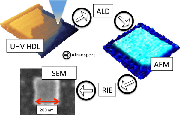
Figure 1. Primary Nanofabrication Process Steps. As an example, a 200 nm x 200 nm square is shown. Each circled arrow indicates a step of atmospheric exposure and transport between sites. After UHV sample prep, the sample is patterned using UHV HDL followed by STM metrology (top left). ALD is then performed, followed by AFM metrology (right). RIE transfers the patterns into Si(100), followed by SEM metrology (bottom left). Please click here to view a larger version of this figure.
The most precise lithography to date usually involves scanned probe techniques, specifically STM-based patterning where atomic resolution patterning and functionalization has been demonstrated for many applications.7 Previously, atom manipulation has produced nanostructures with ultimate precision by using individual atoms as building blocks,8,9,10 but the nanostructures required cryogenic conditions and thus lacked long-term robustness. RT atom manipulation by removal of hydrogen atoms from the surface has been shown, specifically HDL.11,12,13 HDL promises to enable new classes of electronic and other devices based on the spatial localization of surface contrast. Using HDL without further processing, various device architectures are possible including dangling bond wires or logic devices.14,15,16 In addition to providing electrical contrast, HDL can introduce chemical contrast on the surface where the passivating H layer has been removed, in effect creating a template for further chemical modification. This chemical modification has been demonstrated on silicon and other surfaces, showing selectivity for deposition of metals,17 insulators,18 and even semiconductors.16,19 Each of these examples produces two dimensional structures, so other processing steps must be used to produce true three dimensional structures with the atomically resolved control promised by HDL. Previously, this has required repeated patterning,19,20,21 annealing,22 or less well resolved processes such as tip-based e-beam induced deposition.23
Similar to e-beam lithography, HDL uses a localized flux of electrons to expose a resist. Several similarities exist such as the capacity to perform multi-mode lithography with variable spot size and patterning efficiency.24 However, the true power of HDL arises from how it differs from e-beam lithography. First, the resist in HDL is a monolayer of atomic hydrogen so that resist exposure becomes a digital process; the resist atom either is or is not present.25 Since the H atom placement corresponds to the underlying Si(100) lattice the HDL process can be an atomically precise process, although it should be noted that in this paper the HDL has nanometer precision as opposed to having atomic perfection and thus is not digital in this case. Since the electron source in HDL is local to the surface, the various modes of STM operation facilitate both throughput optimization as well as error checking. At tip-sample biases below ~4.5 V, lithography may be performed at the single atom level with atomic precision, known as Atomically Precise mode (AP mode). In contrast, at biases above ~7 V, electrons are emitted directly from the tip to the sample with wide linewidths and high depassivation efficiencies, known here as Field Emission mode (FE mode). HDL throughputs can then be optimized by careful combination of these two modes, although the overall throughputs remain small relative to e-beam lithography with patterning up to 1 μm2/minute possible. When the bias is reversed so that the sample is held at ~-2.25 V, electrons tunnel from the sample to the tip with extremely low depassivation efficiency, thus permitting inspection of the atomic structure of the surface both for error correction and for atomic scale metrology.
This nanostructure fabrication process shown in Figure 1 starts with an UHV-HDL step, as described above. Following HDL, the sample is vented to atmosphere, at which time the patterned areas become saturated with water, forming a thin (i.e., ~1 monolayer) SiO2 layer.26 After transport, the sample is inserted into an ALD chamber for deposition of titania (TiO2), with thicknesses around 2-3 nm deposited here, as measured by AFM and XPS.27 Since the titania reaction depends upon a water saturation of the surface, this process is possible despite atmosphere exposure which saturates the surface with water. Next, to transfer the ALD mask pattern into the bulk the sample was etched using RIE so that 20 nm of Si is removed, with the etch depth determined by AFM and SEM. In order to facilitate metrology steps, an Si(100) wafer is patterned with a grid of lines which are designed to be visible after UHV preparation by a long working distance optical microscope, AFM plan-view optical imaging, and low-magnification plan-view SEM imaging. To help identify the nanoscale structures, 1 μm2 serpentine patterns (serps) are patterned onto the samples with the most isolated nanopatterns located at fixed locations relative to the serps.
This combination of HDL, selective ALD, and RIE can be an important process for nanostructure fabrication, and it includes an atomic scale metrology as a natural byproduct of the process. Below, we include a detailed description of the steps involved to fabricate sub-10 nm nanostructures in Si(100) using HDL, selective ALD, and RIE. It is assumed that one is skilled in each of these processes, but information will be included related to how to integrate the various processes. Particular emphasis will be given to those unexpected difficulties experienced by the authors in order to prevent the same difficulties, especially related to transport and metrology.
Access restricted. Please log in or start a trial to view this content.
Protocol
1. Ex-Situ Sample Preparation
- Prepare chips
- Design appropriate etch mask to put identifying markers in the Si(100) wafer. Using standard optical lithography and RIE, etch a grid of lines as fiducial marks into the wafer from which STM samples will be taken. The lines should be 10 μm wide, 1 μm deep, and at pitch of 500 μm. After etching, strip remaining photoresist from sample.
Note: The fiducial marks must be identifiable in-situ for tip location on the sample as well as in AFM and SEM during metrology. - Protect wafer surface by applying standard tack blue dicing tape, tacky side down.
- Dice wafers into chips using a diamond tipped ceramic dicing saw into sizes appropriate for the specific UHV-STM tool being used to perform HDL. Here, the samples were 8.1 mm x 8.1 mm squares.
- Design appropriate etch mask to put identifying markers in the Si(100) wafer. Using standard optical lithography and RIE, etch a grid of lines as fiducial marks into the wafer from which STM samples will be taken. The lines should be 10 μm wide, 1 μm deep, and at pitch of 500 μm. After etching, strip remaining photoresist from sample.
- After dicing, prepare chip for insertion into UHV-STM patterning tool by gently peeling back the dicing tape, taking care not to touch chip with any nickel-containing tools which will induce an unfavorable surface reconstruction after UHV prep in section 2 below.
- Clean chip by rinsing the front face for 10 sec each with streams of acetone, isopropyl alcohol, methanol, and deionized water, respectively, while gripping the sides of the sample with polytetrafluoroethylene (PTFE) tweezers. Finally, dry with ultrapure N2 or Ar, still gripping with Teflon tweezers.
- Mount sample chip in STM sample holder using methods appropriate for the specific UHV-STM tool to be used for HDL.
- If mounting in a nickel-containing sample holder, cut tantalum foil barrier strips (appx. 4 mm by sample height) using titanium scissors. Sonicate foil strips for 5 min each in ultrapure acetone, isopropyl alcohol, methanol, and DI water, respectively. Dry with ultrapure N2 gas by partially covering a beaker with aluminum foil and injecting an N2 nozzle into the opening. Flow gas until all liquid has evaporated. Using nickel free tweezers, form foil around ends of sample then clamp in sample holder to isolate front and back sides of sample from sample holder.
- After mounting, plasma clean sample and sample holder in oxygen plasma to remove carbon contamination.28
2. UHV Sample Preparation
- Introduce sample into UHV system via load-lock or another preferred UHV-safe method so that the UHV processing and HDL can typically remain below 1.3 x 10⁻⁹ mbar (except for step 2.5.1.1 below).
- Degas O/N at 650 °C, monitoring the temperature with a pyrometer. Ensure that the chamber pressure is within 25% of background. In the case described here, typical background pressures are approximately 4.5 x 10⁻¹⁰ mbar.
- Degas tungsten hydrogen cracking filament at 1,500 °C for 5 min. Activate titanium sublimation pumps if possible.
- Perform sample “Flash” cycle.
- Flash sample by heating to 1,250 °C for 20 sec, monitoring T with pyrometer and using a 10 °C/sec heating gradient. Do not exceed a maximum pressure of 7 x 10⁻⁹ mbar. Cool by removing heating current in less than 5 sec.
- Rest sample at 350 °C for 5 min. to allow pressure to recover to baseline. Repeat 3x.
- Perform sample passivation.
- Set sample temperature to 350 °C using a pyrometer to monitor the temperature. Introduce 1.3 x 10⁻⁶ mbar ultra-pure H2 into prep chamber using leak valve.
- Put a cold trap on the H2 line very near a leak valve in the system in order to further purify H2.
- If possible, pump system with high-velocity turbo pump instead of an ion pump. This is so the ion pump does not contaminate the sample from being exposed to the high pressured and ejecting contaminants. The pumps are put back in the normal state after most the hydrogen has been removed and the sample is still warm (350 °C).
- Turn on tungsten hydrogen cracking filament to a temperature of 1,400 °C for 12 min, then turn off filament and H2 gas flow. Cool sample to RT.
- Set sample temperature to 350 °C using a pyrometer to monitor the temperature. Introduce 1.3 x 10⁻⁶ mbar ultra-pure H2 into prep chamber using leak valve.
3. Scanning Tunneling Microscopy and Lithography
- Transfer sample to STM, and bring sample and STM tip into tunneling range. Using a camera with resolving power of better than a 20 μm spot size, take high-resolution optical image of tip-sample junction. Deskew and resize the optical image so that it represents an undistorted reproduction of the fiducial marks.
- Remove any illumination to reduce system thermal instabilities. Determine surface quality.
- Using conventional STM techniques with sample bias of -2.25 V and 200 pA, identify the number of defects on the surface.
- If surface defects are below acceptable levels, move to the next step. Maximum acceptable defect levels are as followed: Dangling bonds of 1%; Si vacancies of 3%; contaminants of 1%.
- Design HDL patterns to be produced, including both experimental patterns and large (1 μm x 1 μm) serp identification patterns. The serp patterns should be drawn with a long vector axis perpendicular to expected AFM fast scan axis, using a pitch of 15-20 nm. Fracture overall pattern into fundamental shapes to define the path followed by the tip when applying HDL conditions.24
- Using vector outputs from the previous step, perform HDL using FE mode lithography for large areas with sample bias of 7-9 V, current of 1 nA, and 0.2 mC/cm and AP mode lithography for small areas or those areas requiring atomic precision edges.24
- Determine optimal AP mode lithography conditions by performing HDL with an variety of conditions with sample bias ranging from 3.5 to 4.5 V, current ranging from 2 to 4 nA, and line dosages ranging from 2 to 4 mC/cm. Choose conditions that produce the narrowest completely depassivated line.
- Perform STM metrology on desired HDL patterned areas by imaging at -2.25 V sample bias and 0.2 nA tunneling current.
- [optional] Perform error correction. After STM metrology, compare depassivation pattern in the STM images with the desired pattern from step 3.5. If any areas show insufficient dangling bond formation, repeat the lithography cycle in those areas.
- After completing STM HDL, disengage tip from sample, and move sample to load lock.
- Vent and remove sample. During vent with ultrapure N2, protect sample by contacting it with inert, flat substrate such as clean sapphire.29 After surface protection, close valves to any pumps then introduce vent gas as quickly as possible. Remove sample from system.
4. Sample Transport
- Remove sample from load lock. Release sample from sample holder, including removing the foil barrier pieces if possible. Using PTFE (or Ti) tweezers, move sample to transporter, keeping front side of sample protected, attempting to keep atmosphere exposure to less than 10 min.
- Install cover over sample and loosely assemble a pressurized sample transporter. Flush with ultrapure Ar for 1 min. Do not evacuate system at any point, or surface damage may occur.29 Finally, seal sample transporter with a small positive pressure (~50-100 mbar) of Ar so that the sample remains stable for up to a month.
5. Atomic Layer Deposition
- Ensure the ALD is at the proper deposition temperature (100 °C). Slowly increase the argon pressure in the ALD chamber until atmospheric pressure has been achieved.
- Open ALD chamber.
- Open sample transporter and quickly transfer to ALD chamber using a pair of PTFE tweezers grasping the sample on edge, then close the ALD chamber and purge using a flow of argon at a pressure of < 2 × 10⁻¹ mbar for 1 hr to degas the sample. Set a process to perform 80 repeated cycles of ALD to grow 2.8 nm of amorphous titania.
- Using an unmodified commercial ALD system at a sample temperature of 100-150 °C, with titanium tetrachloride (TiCl4) and water (H2O) as precursors perform deposition with reactants at pressures of 0.3 mbar and 0.8 mbar, with pulse times of 0.1 sec and 0.05 sec, respectively.27
- Following each gas pulse, purge the reactor with Ar for 60 sec at 0.2 mbar to ensure minimal background deposition due to physisorbed reactants. For the masks in this work, 80 ALD cycles are used to grow approximately 2.8 nm of amorphous titania at 100 °C.
- Slowly vent ALD chamber with Ar gas and open. Repeat steps 4.1 and 4.2 for sample transport.
6. Atomic Force Microscopy (AFM)
- Ensure proper calibration of the AFM according to manufacturer’s protocol. Open sample transporter and gently remove sample using tweezers.
- After removing from transporter, securely install the sample into the AFM using a mechanical mounting method such as a clamping system if possible. Focus the AFM camera onto the sample, and locate the fiducial markings on the sample surface to align the AFM tip to the pattern based on the optical metrology in step 3.2.
- Ensure that the AFM settings will show both the height and phase information and set the scan size to be between 20 and 40 μm wide. Engage the AFM tip onto the sample.
- Using the height and phase information at highest resolution, scan until the locator patterns region are identified. Zoom into the patterned region and locate the region in which an image is desired.
- Take an image of the desired regions using the appropriate image quality and resolution (typically the highest possible). Once all desired regions have been scanned, disengage the tip from the sample. Unload the sample. Repeat steps 4.1 and 4.2 for sample transport.
7. Reactive Ion Etching
- Chill capacitively coupled RIE reactor to -110 °C, then load the sample into its intro chamber and pump down to 7.5 x 10⁻⁶ mbar.
- Stabilize the temperature for 3 min. Then turn the gas on with flow rates of O2 at 8 sccm (standard cubic centimeter per minute), Ar at 40 sccm, and SF6 at 20 sccm.
- Strike plasma using a 150 W RF discharge, then modify the gas flow to etch for 1 min using SF6 at 52 sccm and O2 at 8 sccm. Interaction of these gases with Si will etch at a rate of approximately 20 nm/min.30
- Pump vacuum to 7.5 x 10⁻⁶ mbar. Vent RIE system. Repeat steps 4.1 and 4.2 for sample transport.
8. Scanning Electron Microscopy (SEM)
- SEM Sample Mounting and introduction of sample to system.
- Place non-adhesive sample mount into a convenient location to facilitate sample mounting.
- Open sample transporter and gently remove sample using tweezers to grab the sample by the edges and securely install into SEM mount, then introduce sample assembly into SEM.
- Vent and open SEM chamber. Securely install sample assembly to the SEM sample stage. Pump down SEM chamber.
- Locate the fiducials.
- Bring the magnification to lowest possible value. Select the accelerating voltage and beam current settings that would give good resolution. Start with lowest acceptable settings. Go up as needed.
- Turn on the electron beam. Bring the general region of interest to recommended working distance and eucentric height.
- Locate and focus on fiducials described in section 1.1. Adjust working distance as necessary. Optimize the focus, brightness and contrast.
- Locate and image the patterns.
- Relative to the fiducials, locate the patterns based on the optical metrology of section 3.2 and AFM metrology of section 6. To minimize carbon deposition on patterns, optimize focus using nearby non-essential features. Once optimized, move to the patterns and acquire plan view images and measurements.
- If needed, tilt the sample for 3D images and pattern height measurements. For other patterns, repeat from 8.3 as needed.
- Perform SEM system closing routine and dismount sample/s, as prescribed by the SEM manufacturer. Secure the sample back into the transporter.
- Repeat steps 4.3 and 4.4 for sample transport and storage. At this point, the samples are robust and can be stored for an indefinite period of time. Perform post-imaging analyses if necessary.
Access restricted. Please log in or start a trial to view this content.
Results
In the cases described here, HDL is performed using multi-mode lithography.24 In FE mode, performed with 8 V sample bias, 1 nA, and 0.2 mC/cm (equivalent to 50 nm/sec tip speed), the tip moves over the surface either parallel or perpendicular to the Si lattice, producing lines of depassivation. While this lineshape is very tip dependent, in the case here, the completely depassivated portion of the lines was approximately 6 nm wide, with tails of partial depassivation extending another 2 nm on either side of th...
Access restricted. Please log in or start a trial to view this content.
Discussion
Performing metrology on the nanostructures described above requires the ability to bridge the tip positioning during HDL and pattern location using other tools such as AFM and SEM. In contrast to other well-developed patterning tools with high-resolution position encoding such as e-beam lithography, the HDL performed here was performed with an STM without well controlled coarse positioning, so extra position identification protocols were used, as shown in Figure 3. First, a long-focal-length microscope i...
Access restricted. Please log in or start a trial to view this content.
Disclosures
The authors have nothing to disclose.
Acknowledgements
This work was supported by a Contract from DARPA (N66001-08-C-2040) and by a grant from the Emerging Technology Fund of the State of Texas. The authors would like to acknowledge Jiyoung Kim, Greg Mordi, Angela Azcatl, and Tom Scharf for their contributions related to selective atomic layer deposition, as well as Wallace Martin and Gordon Pollock for ex-situ sample processing.
Access restricted. Please log in or start a trial to view this content.
Materials
| Name | Company | Catalog Number | Comments |
|---|---|---|---|
| Si Wafer | VA Semiconductor | P type (Boron) Si<100> ± 2 degrees, 280 mm ± 25 mm thick, 0.01-0.02 ohm-cm | |
| Ta foil | Alfa Aesar | 335 | 0.025 mm (0.001 in) thick, 99.997% (metals basis) |
| Methanol | Alfa Aesar | 19393 | Semiconductor Grade, 99.9% |
| 2-Propanol | Alfa Aesar | 19397 | Semiconductor Grade, 99.5% |
| Acetone | Alfa Aesar | 19392 | Semiconductor Grade, 99.5% |
| Argon | Praxair | Ultra high purity (grade 5.0) | |
| Deionized water | Millipore | Milli-Q Water Purification System | >18 MW resistance water produced on demand. |
| TiCl4 | Sigma Aldrigh | 254312 | ≥99.995% trace metals basis |
| O2 | Matheson | G2182101 | Research Grade |
| SF6 | Matheson | G2658922 | Ultra high purity (grade 4.7) |
| Blue Medium Tack Roll | Semiconductor Equipment Corporation | 18074 | Thickness 75 μm / 0.003” Length 200 M / 660’ |
References
- Yoffe, A. D. Low-dimensional systems: quantum size effects and electronic properties of semiconductor microcrystallites (zero-dimensional systems) and some quasi-two-dimensional systems. Adv. in Phy. 42 (2), 173-262 (1993).
- Alivisatos, A. P. Semiconductor Clusters, Nanocrystals, and Quantum Dots. Science. 271 (5251), 933-937 (1996).
- Craighead, H. G. Nanoelectromechanical Systems. Science. 290 (5496), 1532-1535 (2000).
- Dai, M. D., Kim, C. -W., Eom, K. Finite size effect on nanomechanical mass detection: the role of surface elasticity. Nanotechnology. 22 (26), 265502(2011).
- Personick, M., Mirkin, C. Making sense of the mayhem behind shape control in the synthesis of gold nanoparticles. J. Am. Chem. Soc. 135 (C), 18238-18247 (2013).
- Rothemund, P. W. K., Ekani-Nkodo, A., et al. Design and Characterization of Programmable DNA. Nanotubes. J. Am. Chem. Soc. 26, 16344-16353 (2004).
- Hersam, M. C., Guisinger, N. P., Lyding, J. W. Silicon-based molecular nanotechnology. Nanotechnology. 11 (2), 70-76 (2000).
- Eigler, D. M., Schweizer, E. K. Positioning single atoms with a scanning tunnelling microscope. Nature. 344, 524-526 (1990).
- Heinrich, A. J., Lutz, C. P., Gupta, J. A., Eigler, D. M. Molecular cascades. Science. 298, 1381-1387 (2002).
- Crommie, M. F., Lutz, C. P., Eigler, D. M. Confinement of Electrons to Quantum Corrals on a Metal Surface. Science. 262 (5131), 218-220 (1993).
- Shen, T. -C., Wang, C., et al. Atomic-Scale Desorption Through Electronic and Vibrational Excitation Mechanisms. Science. 268, 1590-1592 (1995).
- Randall, J. N., Lyding, J. W., et al. Atomic precision lithography on Si. J. Vac. Sci. Tech. B. 27 (6), 2764-2768 (2009).
- Tong, X., Wolkow, R. A. Electron-induced H atom desorption patterns created with a scanning tunneling microscope: Implications for controlled atomic-scale patterning on H-Si(100). Surf. Sci. 600 (16), L199-L203 (2006).
- Hitosugi, T., Hashizume, T., et al. Scanning Tunneling Spectroscopy of Dangling-Bond Wires Fabricated on the Si(100)-2x1-H Surface. Jap. J. App. Phys, Pt 2 2. 36 (3B), L361-L364 (1997).
- Bird, C. F., Fisher, A. J., Bowler, D. R. Soliton effects in dangling-bond wires on Si(001). Phys. Rev B. 68, 115318(2003).
- Wolkow, R. A., Livadaru, L., et al. Beyond-CMOS Electronics. , Available from: http://arxiv.org/abs/1310.4148 1-28 (2013).
- Lyding, J. W., Shen, T. -C., Hubacek, J. S., Tucker, J. R., Abeln, G. C. Nanoscale patterning and oxidation of H-passivated Si(100)-2×1 surfaces with an ultrahigh vacuum scanning tunneling microscope. App. Phys. Lett. 64 (15), 2010-2012 (1994).
- Lyding, J. W., Shen, T. -C., Abeln, G. C., Wang, C., Tucker, J. R. Nanoscale patterning and selective chemistry of silicon surfaces by ultrahigh-vacuum scanning tunneling microscopy. Nanotechnology. 7, 128-133 (1996).
- Owen, J. H. G., Ballard, J., Randall, J. N., Alexander, J., Von Ehr, J. R. Patterned Atomic Layer Epitaxy of Si / Si(001):H. J. Vac. Sci. Tech. B. 29 (6), 06F201(2011).
- Goh, K. E. J., Chen, S., Xu, H., Ballard, J., Randall, J. N., Ehr, J. R. Von Using patterned H-resist for controlled three-dimensional growth of nanostructures. App. Phys. Lett. 98 (16), 163102(2011).
- Ye, W., Peña Martin, P. Direct writing of sub-5 nm hafnium diboride metallic nanostructures. ACS Nano. 4 (11), 6818-6824 (2010).
- Brien, J. L., Schofield, S. R., et al. Scanning tunnelling microscope fabrication of arrays of phosphorus atom qubits for a silicon quantum computer. Smart. 11 (5), 741-748 (2002).
- Van Oven, J. C., Berwald, F., Berggren, K. K., Kruit, P., Hagen, C. W. Electron-beam-induced deposition of 3-nm-half-pitch patterns on bulk Si. J. Vac. Sci. Tech. B. 29 (6), 06F305(2011).
- Ballard, J. B., Sisson, T. W., et al. Multimode hydrogen depassivation lithography: A method for optimizing atomically precise write times. J. Vac. Sci. Tech. B. 31 (6), 06FC01(2013).
- Randall, J. N., Ballard, J. B., et al. Atomic precision patterning on Si: An opportunity for a digitized process. Microelec. Eng. 87 (5-8), 955-958 (2010).
- Perrine, K. A., Teplyakov, A. V. Reactivity of selectively terminated single crystal silicon surfaces. Chem. Soc. Rev. 39 (8), 3256-3274 (2010).
- McDonnell, S., Longo, R. C., et al. Controlling the Atomic Layer Deposition of Titanium Dioxide on Silicon: Dependence on Surface Termination. The J. Phys. Chem. C. 117 (39), 20250-20259 (2013).
- Kane, D. F. Plasma cleaning of metal surfaces. J. Vac. Sci. Tech. 11 (3), 567(1974).
- Hersam, M. C., Guisinger, N. P., Lyding, J. W., Thompson, D. S., Moore, J. S. Atomic-level study of the robustness of the Si(100)-2×1:H surface following exposure to ambient conditions. App. Phys. Lett. 78 (7), 886-888 (2001).
- Agostino, R., Flamm, D. L. Plasma etching of Si and SiO2 in SF6–O2 mixtures. J. App. Phys. 52 (1), 162(1981).
- Longo, R. C., McDonnell, S., et al. Selectivity of metal oxide atomic layer deposition on hydrogen terminated and oxidized Si(001)-(2×1) surface. J. Vac. Sci Tech. B. 32 (3), 03D112(2014).
- Ruess, F. J., Oberbeck, L., et al. The use of etched registration markers to make four-terminal electrical contacts to STM-patterned nanostructures. Nanotechnology. 16 (10), 2446-2449 (2005).
- Ruess, F. J., Pok, W., et al. Realization of Atomically Controlled Dopant Devices in Silicon. Small. 3 (4), 563-567 (2007).
- Li, K., Namboodiri, P., et al. Controlled formation of atomic step morphology on micropatterned Si (100). J. Vac. Sci. Tech. B. 29 (4), 041806(2011).
- Ballard, J. B., Owen, J. H. G., et al. Pattern transfer of hydrogen depassivation lithography patterns into silicon with atomically traceable placement and size control. Journal of Vacuum Science and Technology B. 32 (4), 041804(2014).
- Gusev, E. P., Cabral, C. Jr, Copel, M., D’Emic, C., Gribelyuk, M. U ltrathin HfO 2 films grown on silicon by atomic layer deposition for advanced gate dielectrics applications. Microelectronic Engineering. 69, 145-151 (2003).
Access restricted. Please log in or start a trial to view this content.
Reprints and Permissions
