This paper investigates the suitability of inkjet printing for the manufacturing of dye-sensitized solar cells. A binder-free TiO2 nanoparticle ink was formulated and printed onto a FTO glass substrate. The printed layer was fabricated into a cell with an active area of 0.25 cm2 and an efficiency of 3.5%.
Method Article
Digital Printing of Titanium Dioxide for Dye Sensitized Solar Cells
In This Article
Summary
Abstract
Silicon solar cell manufacturing is an expensive and high energy consuming process. In contrast, dye sensitized solar cell production is less environmentally damaging with lower processing temperatures presenting a viable and low cost alternative to conventional production. This paper further enhances these environmental credentials by evaluating the digital printing and therefore additive production route for these cells. This is achieved here by investigating the formation and performance of a metal oxide photoelectrode using nanoparticle sized titanium dioxide. An ink-jettable material was formulated, characterized and printed with a piezoelectric inkjet head to produce a 2.6 µm thick layer. The resultant printed layer was fabricated into a functioning cell with an active area of 0.25 cm2 and a power conversion efficiency of 3.5%. The binder-free formulation resulted in a reduced processing temperature of 250 °C, compatible with flexible polyamide substrates which are stable up to temperatures of 350 ˚C. The authors are continuing to develop this process route by investigating inkjet printing of other layers within dye sensitized solar cells.
Introduction
Conventional silicon solar cells are made from highly pure materials that require expensive and high-energy consuming specialist equipment. These conventional silicon cells incorporate a p-n junction that requires highly pure materials at the interface to generate electron-hole pairs. Dye-sensitized solar cells (DSSCs) have a fundamentally different working principle, where charge generation takes place at the materials interface. This means that processing under vacuum, ultrahigh temperatures or the use of clean room facilities are not required1. Therefore they are seen as a potentially low cost alternative; however up-scaling from small laboratory test cells into large prototypes for industrial manufacturing involves overcoming several issues including the rapid patterning of substrates.
Electronics manufacturing generally requires a degree of patterning, which is either achieved by masking or selective removal of the material after deposition. These steps can be removed through the use of "additive" digital printing techniques such as inkjet printing or spray coating. Digital printing is a promising method for direct deposition of functional materials for electronic devices. The technique can be described as printing from a digital-based pattern directly to a variety of substrates2. They are non-contact methods, which will not damage or contaminate the substrate surface and deposit material only where it is required, resulting in little or no wastage3. These techniques have been highlighted as being ideally suited to being scaled up to high-volume production3. Since digital printing methods use liquid forms of materials dispersed in a solvent, it is critical to understand the deposition of ink to determine the applications of the technique.
DSSCs have three main components: a porous layer of wide bandgap metal oxide material, a dye that covers the particles, and a "charge transporter" that infiltrates the pores within the porous layer of semiconductor. These are sandwiched in between a transparent conductive electrode and a counter electrode4. The counter electrode is coated with a catalytic material for electron transfer, which in most cases is platinum. Under illumination, the dye molecules will absorb energy in the form of photons. The dye molecules then become excited and charge separation occurs at the interface of the titanium dioxide and the dye. Electrons are ejected into the adjacent metal oxide particles and 'holes' are left behind on the dye molecule. The injected electrons travel through the metal oxide particles and reach the transparent conductive electrode. When a load is connected, the electrons move to the counter electrode through the external circuit and are finally reunited with their counter charges through the redox couple present in the electrolyte1. The nano-structured metal oxide layer within DSSCs plays a critical role in the overall performance of the cell, with material choice, processing methods and nature of the structure all having influencing factors5-10. One of the most important requirements for the photoanode is that it needs to have an extremely large surface area. This is achieved through the deposition of nanoparticle materials, commonly TiO21,11. This has been fabricated by countless different processes, however wet coating techniques such as screen-printing and doctor-blading, are still the most popular approach9,12,13.
Inkjet technology is a potential manufacturing route for dye-sensitized solar cells. It uses the movement of a piezoelectric crystal to expel a fixed quantity of liquid through a nozzle onto the desired substrate. This deposition method allows material to be jetted very accurately but also at high frequency with a potentially high print speed or deposition rate. Inkjet technology is sensitive to the viscosity of the ink used and this was previously a barrier to the development of functional inks. Recent work in the development of solvents suitable for ink formulation has helped to alleviate this problem, and printing of electronic components using 2D layered materials such as graphene has been demonstrated14. The viscosity of nanoparticle suspensions such as these has been found to depend on the nanoparticle size and concentration15. High concentrations of nanoparticles result in higher viscosities, therefore particle loadings are usually around 10 wt% to avoid nozzle blockages16, however higher concentrations have been achieved17.
The key advantages of inkjet technology include it being non-contact, additive patterning and maskless18. The latter two attributes are due to the ability to position many nozzles together on one or more printheads, with each nozzle separately addressable by the control software. This allows highly complex, multi-layered patterns to be created very rapidly as the printheads move across the substrate. No masking between materials or layers is required as the position of each ink drop is accurately controlled, in some systems to an accuracy of ~1.5 µm19. One of the key benefits is that inkjet technology is mature, with significant development carried out in the latter half of the twentieth century. The result is that the inkjet is a very scalable technology, with roll-to-roll systems capable of printing accurately onto flexible substrates at rates of many meters per second. Traditionally this was used for high volume production, e.g., newspapers. However, developments in technology have allowed the inkjet to be used in roll-to-roll production of electronic circuits using nanoparticulate silver inks20. The inkjet is therefore an attractive process for the potential production of dye-sensitized solar cells by digital printing.
Protocol
1. Ink Formulation
Note: Ink formulations are often kept a highly guarded secret by manufacturers. Successful formulations balance jetting, drop formation, wetting and drying behavior alongside functional performance. Usually a functional material is dispersed in a solvent and at least one other component to make them jettable. This section details the development of a TiO2 ink for use within inkjet printing. A small batch of ink was prepared by the following method.
Caution: Ink preparation should be performed in a suitably vented area, e.g., under a fume hood, whilst wearing eye protective goggles and latex gloves.
- Prepare a 0.1 mM aqueous solution of hydrochloric acid (HCl) to produce a pH of approximately 4.
- Add 32 g of the acid solution to 8 g of a compatible solvent with a higher boiling point and lower surface tension than water (such as dimethylformamide (DMF)). The addition of a co-solvent acts as a drying agent to induce a circulating flow within the ink droplet as the ink evaporates, leading to a uniform placement of nanoparticles over the surface of the droplet 21.
- Add 1.5 g of dispersing additive (45% active solution of propylene glycol and tetramethyl-5-decyne-4,7-diol in water).
- Add 10 g of ethylene glycol, as a humectant to prevent drying at the nozzles.
- Add 0.5 g of defoaming agent (20% active solution of acetylenic diol in methoxypolyethyleneglycol) to the ink to prevent air bubbles from developing.
- Perform a simple shake test by taking an aliquot of the ink into a closed container and shake by hand for 60 sec. If any foam is observed then add another 0.5 g of defoaming agent to the ink.
- Mix the solution for 8 hr using a magnetic stirring bar to ensure homogeneity at RT.
- Add 1.5 g of titanium dioxide (TiO2) nanoparticles with a primary particle size of 21 nm and surface area of 35 - 65 m2/g.
- Sonicate the mixture using an ultrasonic probe for 15 min at a frequency of 60 Hz.
- Measure the particle sizes, using an appropriate measurement technique such as dynamic light scattering (DLS) according to manufacturer's protocol, to ensure that they will flow easily through the nozzle openings. Make measurements under the same conditions (e.g., same solvent, pH, concentration of dispersant) to be used for the ink as each component may influence the formation of agglomerates within the ink. For successful jetting, the particles within the fluid should be 100 times smaller than the nozzle opening.
- Measure the viscosity of the ink, using an appropriate measurement technique such as a rotational viscometer according to manufacturer's protocol, to ensure reliable jetting from the printhead as inkjet printing requires low viscosity inks of between 2 and 20 centipoise (cP). Increase the viscosity through the addition of polymeric materials or cellulose-based materials; however these need to be removed after deposition to free up sites for the dye within the printed film22.
- Measure the surface tension of the ink, using an appropriate measurement technique such as a tensiometer according to manufacturer's protocol, to ensure reliable jetting. The jettable fluid formulation guidelines for inkjet printers suggest a surface tension between 28 and 33 mN/m to enable reliable printing.
2. Inkjet Printing
- Prior to printing, soak the glass substrates in a 2 wt% solution of cleaning detergent (a mixture of anionic and non-ionic surface active agents, stabilizing agents, alkalis, non-phosphate detergent builders and sequestering agents, in an aqueous base) in deionized water. Rinse the glass thoroughly with deionized water as soon as they are removed from the cleaning solution to remove traces of contamination and cleaning detergent.
- Measure the surface energy of the substrate, using an appropriate measurement technique such as a tensiometer according to manufacturer's protocol. For good adhesion, the surface energy of the substrate should not exceed the surface tension of the fluid by more than 10 - 15 mN/m. Modify the surface energy of the substrate using methods such as corona treatment23, plasma treatment24 and chemical etching25 if it is not suitable.
- Load the substrate into the printer according to manufacturer's protocol.
- Flush the print head with the ink through the port located on the side of the head to displace any air or cleaning solution within the reservoir and nozzles.
- Insert the printhead into the printer. Connect the printhead with the head personality board.
- Filter the ink through the correct size filter just before loading into the cartridge to remove large particle aggregates which can clog the nozzles. The printhead used in this work (e.g., Konica KM512) has nozzles with a diameter of 40 µm; therefore inks should not contain particles with a diameter more than 400 nm. Pass the suspensions through a 5 µm, followed by a 1.2 µm polyvinylidene fluoride (PVDF) filter to remove any large particulates.
- Load the ink into the 150 ml syringe located above the print head, which supplies the ink to the print head. Attach the airtight cap on top of the syringe and turn on the vacuum pump.
- Purge the ink through the nozzles by pressing the 'purge' button located on the vacuum pump.
- Through the geographic information system (GIS) print server, set-up the waveform and printing parameters. Note that the printer can print up to a speed of 1.5 meters per second, however for this ink a print speed of 0.3 meters per second has been found to provide optimal coating
- Open GIS user interface software and load the desired pattern.
- Print from the loaded cartridge according to manufacturer's protocol.
- Remove the substrate from the platen and heat the printed films at 150 ºC for 30 min, followed by 250 ºC for a further 30 min either on a hot plate or in an oven.
3. Analysis of the Printed Films
- Use an optical microscope or a scanning electron microscope (SEM) to look at the surface of the printed films at low magnification (100X) to analyze the surface morphology and at high magnification (35,000X) to analyze the porosity of the printed films. Check that the images show a uniform coverage with no cracks and good porosity. More detailed information on SEM operation can be found in the following references26,27.
- Measure the thickness of the printed layer, using an appropriate measurement technique such as a surface profiler according to manufacturer's protocol. The thickness and porosity of the TiO2 layer within DSSCs influence the amount of dye that can be absorbed onto the surface of the nanoparticles, which therefore influence the overall electrical conversion efficiency of the cell18. It is therefore an important parameter to evaluate. Use a surface profiler (precision of 1 nm) to measure the thickness of the printed films.
- Measure the transmittance of the film, using an appropriate measurement technique such as an ultraviolet-visible (UV-VIS) spectrophotometer to determine how much visible light will transmit through the printed film. Use manufacturer's protocol.
4. Making the Cell
- Make a dye solution by mixing 20 ml of ethanol and 2 mg of ruthenium dye in a glass beaker using a magnetic stirrer for 8 hr.
- Submerge the TiO2 coated glass in the solution at RT (20 to 25°C) for 24 hr to allow the dye to absorb onto the surface of the TiO2 particles.
- Remove the TiO2 coated glass from the solution and place onto tissue paper to soak up any excess dye solution (with the TiO2 facing upwards to avoid contamination).
- Place the pre-cut 60 µm thick thermoplastic sealing spacer on top of the conductive glass, around the TiO2 coating.
- Place the platinum coated counter electrode on top of the pre-cut 60 µm thick thermoplastic sealing spacer so that the active sides of the anode and the cathode are facing each other. Allow enough overlap between the two pieces of glass so that an electrical contact can be made with the conductive glass. This should have a pre-drilled hole in the center to allow for electrolyte filling later.
- Heat on a hot plate to a temperature of 110 ˚C and apply light pressure using tweezers over the area of the sealing spacer. After 30 sec the electrodes should be sealed together.
- Fill the gap between the two electrodes with an iodide/tri-iodide electrolyte in acetonitrile at a concentration of 50 mM, by injecting through the pre-drilled hole in the platinum coated glass using a syringe.
Results
A TiO2 ink was formulated according to the procedure outlined. The size of particles suspended within the ink was measured using dynamic light scattering (DLS) and an average particle size of 80 nanometers (nm) was observed. The viscosity of the ink in this work was found to be 3 cP, measured using a rotational viscometer with a small sample adapter and an 18 mm spindle diameter. The surface tension was measured using a tensiometer and was calculated to be an average of 26 mN/m.
The surface energy of the FTO glass was calculated according to the European Standard EN 828 for determining the wettability of a solid surface by measuring the contact angle and surface free energy. Ten drops of three different liquids (water, ethylene glycol and diiodomethane) were dispensed onto a plane test piece surface. For each drop, the left and right contact angle were measured. From the averaged contact angles of each liquid combined with its surface tension, the surface free energy of the test piece is calculated. The Fowkes method calculates the total surface energy (γ) from the sum of the contributions from dispersive interactions (γd) and γnon-dispersive interactions (γp). This method resulted in a surface free energy of 26.45 mN/m for the FTO coated glass.
Printing was carried out according to the procedure above to produce 5 mm squares. The thickness of the printed layer on the glass was measured using a surface profiler. The maximum thickness at the center of the printed layer was measured to be 2.6 µm. The transmittance of the coated glass was measured using a UV-VIS spectrometer. At a wavelength of 700 nm, a 60% transmittance was measured for the TiO2 printed film compared with 78% for the FTO glass.
Photovoltaic devices were produced according to the procedure outline above and characterized directly after fabrication to minimize the effect of degradation caused by water and oxygen in the air. There are five electrical performance parameters that are used to characterize and compare solar cells28. The values of short circuit current (Isc) and open circuit voltage (Voc) can be derived from the current-voltage (I-V) curve. These can then be used to determine the fill factor (FF) and power conversion efficiency (η). The FF gives a ratio of the cells actual maximum power output to the product of the open circuit voltage and short circuit current29. This is a key parameter in evaluating the performance of solar cells. A high FF means low electrochemical losses, whereas a low FF indicates there is room for improvement. Several factors are known to influence the FF including the quality and interface of layers within the cell. DSSCs incorporating an iodide/triiodide redox couple with record efficiencies of 11.9% report fill factors of 0.7130. All of these parameters need to be determined under standard test conditions where the device temperature is 25 ˚C, spectral irradiance distribution of the light has an air mass of 1.5, total irradiance measured (Em) at the solar cell is 100 mW/cm2 . Theoretical maximum for the conversion efficiency for a single p-n junction cell has been widely reported as 37.7%31, however for DSSCs it has been reported that the maximum efficiency is closer to 15.1% with an absorption onset at 920 nm32.
The output current and voltages were measured using a source meter whilst the cells were illuminated with a 100 mW/cm2 light source fitted with a filter to match the spectral irradiance distribution with an air mass of 1.5. The results were compared to a cell produced using a doctor-bladed TiO2 layer using a commercially available paste which has a blend of anatase particles 20 nm and 450 nm. The printed layer had an area of 0.25 cm2 and an average thickness of 18 µm which was measured using a surface profiler. A comparison of the photoelectric performance between the two devices is shown in Figure 1 and Table 1.
Several studies have investigated the relationship between the thickness of the TiO2 layer and the conversion efficiency within DSSCs. The results vary significantly, with optimum film thickness reported from anywhere between 9.5 µm and 20 µm 33-39. Table 1 outlines the thicknesses of the TiO2 printed layers and the efficiencies. The thickness of the inkjet printed TiO2 is significantly less than the doctor bladed TiO2, resulting in a lower efficiency. Future work will investigate the use of organic binders within the ink formulation to increase the thickness of the inkjet printed layer.
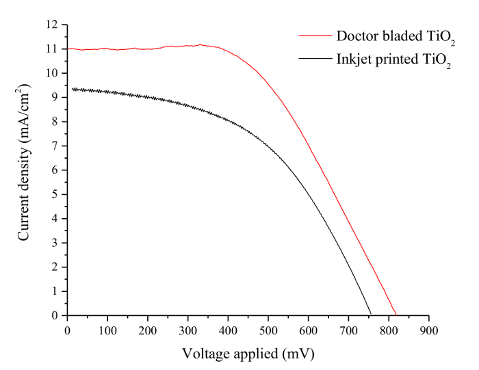
Figure 1. Performance Curves of DSSCs with Inkjet Printed and Doctor Bladed TiO2 Layers. Current-density/voltage curves for DSSCs incorporating an inkjet printed TiO2 layer and a doctor-bladed TiO2 layer. The short circuit current density in the device with the inkjet printed TiO2 layer is significantly lower than the device with the doctor bladed TiO2 layer resulting in a lower overall conversion efficiency. Please click here to view a larger version of this figure.
| Short circuit current | Open circuit voltage | Fill factor | Efficiency | Thickness | |
| (mA/cm2) | (mV) | ||||
| (%) | (µm) | ||||
| Inkjet printed | 9.42 | 760 | 0.49 | 3.5 | 2.6 |
| Doctor bladed | 11 | 756 | 0.58 | 4.8 | 18 |
Table 1. Key Performance Characteristics of the Cells in Figure 1. This table compares the key parameters of the solar cell including open circuit voltage (Voc), short circuit current (Isc) which determine the efficiency (η) under the specified light condition are presented. The parameters of a cell produced using a doctor-bladed TiO2 layer have also been included for comparison. The fill factors (FF) of both devices are quite low which is generally attributed to a high internal resistance within the cell.
Discussion
A particular challenge when formulating inks is the natural tendency for nanoparticles to cluster together. These are known as either aggregates or agglomerates, depending on the nature and strength of the bonds between the particles. The energy of simply stirring particles into water or binder is not great enough to overcome the particle attractive forces preventing the breakup of agglomerates. Ball milling, high shear mixing or ultrasonication are commonly used to break up agglomerated nanoparticles. Various anionic, nonionic, and cationic surfactants and polymers can also be used to provide long-term stabilization. By minimizing the number of these agglomerates, a good quality suspension can be achieved. The fluids should be filtered through the correct size filter just before loading into the cartridge to remove large particle aggregates which can clog the nozzles.
The particle size within the TiO2 layer also has been shown to influence the overall efficiency of DSSCs. The photocatalytic activity of titanium dioxide increases as particle sizes decrease due to an increase in the specific surface area40. A study comparing the efficiency of DSSCs incorporating TiO2 nanoparticles with 5 different sizes ranging from 400 nm to 14 nm and found that those with smaller particle sizes resulted in better electrical conversion efficiencies33.
Inkjet printing is a non-contact deposition technique capable of multi-pass printing. This presents the unique opportunity to rapidly fabricate multilayer devices in one operation on a wide range of substrates with minimal material waste. It also potentially provides a way to integrate other components (such as batteries) into the system through the printing of functional materials41. Although the representative results shown for the inkjet printed devices do not perform as well as the doctor-bladed devices, it demonstrates the potential for the deposition technique. With further ink optimization, it could perform on a comparable level to currently used methods and may provide further scope for cost-effective, environmentally friendly integration of photovoltaic cells onto a wide range of substrates. We hope to improve the efficiency of the inkjet printed devices by increasing the thickness of the printed layer closer to that of the doctor-bladed TiO2 and will continue to look at the printing of other materials and layers within DSSCs.
Disclosures
The authors have nothing to disclose.
Acknowledgements
This research is gratefully undertaken with support from the Engineering and Physical Sciences Research Council (EPSRC) funded through a doctoral training grant. Open access article processing charges (APCs) were funded by Research Councils UK (RCUK). All of the data is provided in full in the results section of the paper. Representative results have previously been published by the authors42.
We would like to thank Dr. Senthilarasu Sundaram from the University of Exeter for his help in characterising the electrical performance of the cells.
Materials
| Name | Company | Catalog Number | Comments |
|---|---|---|---|
| Titanium dioxide | Sigma Aldrich | 718467 | |
| Deionized water | Supplied from a filter in the laboratory | ||
| Hydrochloric acid, 2 M (2 N) | Fisher Scientific | J/4250/17 | |
| Dimethylformamide (DMF) | Fisher Scientific | D/3840/08 | |
| Ethanol | VWR Chemicals | 20721.33 | |
| Dispersing additive | Air Products | ||
| Defoaming agent | Air Products | ||
| Ethylene glycol | Fluka | 107-21-1 | |
| Polyvinylidene fluoride (PVDF) syringe filter | VWR International | ||
| Cleaning detergent | Fisher Scientific | 10335650 | |
| Fluorine doped tin oxide (FTO) glass, 8 Ω/sq | Pilkington | ||
| Ruthenizer dye | Solaronix | 21613 | |
| Pre-cut 60 µm thick thermoplastic sealing film | Solaronix | 74301 | |
| 50 mM Iodide/tri-iodide electrolyte in acetonitrile | Solaronix | 31111 | |
| Platinum coated FTO glass | Solaronix | 74201 | |
| Vac'n'Fill Syringe | Solaronix | 65209 | |
| Polyimide tape (6.35 mm) | Onecall Farnell | 1676087 |
References
- Docampo, P., et al. Lessons Learned: From Dye-Sensitized Solar Cells to All-Solid-State Hybrid Devices. Adv. Mater. 26, 4013-4030 (2014).
- Hudd, A. The Chemistry of Inkjet Inks. Magdassi, S. , 3-18 (2009).
- Krebs, F. C. Fabrication and processing of polymer solar cells: A review of printing and coating. Sol. Energ. Mat. Sol. Cells. 93, 394-412 (2009).
- Reddy, P. J. Solar Power Generation: Technology, New Concepts & Policy. , Taylor & Francis. (2012).
- Gemeiner, P., Mikula, M. Acta. Chem. Slov. 6, 29(2013).
- Xue, Z., Jiang, C., Wang, L., Liu, W., Liu, B. Fabrication of Flexible Plastic Solid-State Dye-Sensitized Solar Cells Using Low Temperature Techniques. J. Phys. Chem. C. 118, 16352-16357 (2014).
- Oh, Y., Yoon, H. G., Lee, S. -N., Kim, H. -K., Kim, J. Inkjet-Printing of TiO2 Co-Solvent Ink: From Uniform Ink-Droplet to TiO2 Photoelectrode for Dye-Sensitized Solar Cells. J. Electrochem. Soc. 159, 34-38 (2011).
- Lin, L. -Y., et al. Low-temperature flexible Ti/TiO2 photoanode for dye-sensitized solar cells with binder-free TiO2 paste. Prog. Photovolt. Res. Appl. 20, 181-190 (2012).
- Gong, J., Liang, J., Sumathy, K. Review on dye-sensitized solar cells (DSSCs): Fundamental concepts and novel materials. Renew. Sustainable Energy Rev. 16, 5848-5860 (2012).
- Bosch-Jimenez, P., Yu, Y., Lira-Cantu, M., Domingo, C., Ayllòn, J. A. Solution processable titanium dioxide precursor and nanoparticulated ink: Application in Dye Sensitized Solar Cells. J Colloid Interf Sci. 416, 112-118 (2014).
- Jose, R., Thavasi, V., Ramakrishna, S. Metal Oxides for Dye-Sensitized Solar Cells. J. Am. Ceram. Soc. 92, 289-301 (2009).
- Gemeiner, P., Mikula, M. Efficiency of dye sensitized solar cells with various compositions of TiO2 based screen printed photoactive electrodes. Acta. Chem. Slov. 6, 29-34 (2013).
- Lee, K. E., Charbonneau, C., Demopoulos, G. P. Thin single screen-printed bifunctional titania layer photoanodes for high performing DSSCs via a novel hybrid paste formulation and process. J. Mater. Res. 28, 480-487 (2013).
- Li, J., Lemme, M. C., östling, M. Inkjet Printing of 2D Layered Materials. ChemPhysChem. 15, 3427-3434 (2014).
- Rudyak, V. Y., Krasnolutskii, S. L. Dependence of the viscosity of nanofluids on nanoparticle size and material. Phys. Lett. A. 378, 1845-1849 (2014).
- Dispoto, G., Moroney, N., Hanson, E., Meyer, J. D., Allen, R. R. Color Desktop Printer Technology Optical Science and Engineering. , CRC Press. 111-155 (2006).
- Hsien-Hsueh, L., Kan-Sen, C., Kuo-Cheng, H. Inkjet printing of nanosized silver colloids. Nanotechnology. 16, 2436(2005).
- Singh, M., Haverinen, H. M., Dhagat, P., Jabbour, G. E. Inkjet Printing: Inkjet Printing-Process and Its Applications. Adv. Mater. 22, 673-685 (2010).
- Stüwe, D., Mager, D., Biro, D., Korvink, J. G. Inkjet Technology for Crystalline Silicon Photovoltaics. Adv. Mater. 27, 599-626 (2015).
- Perelaer, J., et al. Roll-to-Roll Compatible Sintering of Inkjet Printed Features by Photonic and Microwave Exposure: From Non-Conductive Ink to 40% Bulk Silver Conductivity in Less Than 15 Seconds. Adv. Mater. 24, 2620-2625 (2012).
- Hwang, M. -s, Jeong, B. -y, Moon, J., Chun, S. -K., Kim, J. Inkjet-printing of indium tin oxide (ITO) films for transparent conducting electrodes. Mat. Sci. Eng. B. 176, 1128-1131 (2011).
- Hara, K., Arakawa, H. Handbook of Photovoltaic Science and Engineering. , John Wiley & Sons, Ltd. Ch. 15 663-700 (2003).
- Ryu, J., Wakida, T., Takagishi, T. Effect of Corona Discharge on the Surface of Wool and Its Application to Printing. Text. Res. J. 61, 595-601 (1991).
- Yang, L., Chen, J., Guo, Y., Zhang, Z. Surface modification of a biomedical polyethylene terephthalate (PET) by air plasma. Appl. Surf. Sci. 255, 4446-4451 (2009).
- Qian, B., Shen, Z. Fabrication of Superhydrophobic Surfaces by Dislocation-Selective Chemical Etching on Aluminum, Copper, and Zinc Substrates. J. Am. Chem. Soc. 21, 9007-9009 (2005).
- Echlin, P. Handbook of Sample Preparation for Scanning Electron Microscopy and X-Ray Microanalysis. , Springer. (2011).
- Flegler, S. L., Heckman, J. W., Klomparens, K. L. Scanning and Transmission Electron Microscopy: An Introduction. , Oxford University Press. (1993).
- O'Donnell, M. Z. R. How To Minimize Measurement Errors In Solar Cell Testing. Solar Industry Magazine. , http://www.newport.com/images/webdocuments-en/images/Solar_Industry-Solar_Cell_Testing.pdf (2011).
- Grätzel, M. Dye-sensitized solar cells. J. Photochem. Photobiol. C: Photochem. Rev. 4, 145-153 (2003).
- Green, M. A., Emery, K., Hishikawa, Y., Warta, W., Dunlop, E. D. Solar cell efficiency tables (version 46). Prog. Photovolt. Res. Appl. 23, 805-812 (2015).
- Shockley, W., Queisser, H. J. Detailed Balance Limit of Efficiency of p-n Junction Solar Cells. J. Appl. Phys. 32, 510-519 (1961).
- Snaith, H. J. Estimating the Maximum Attainable Efficiency in Dye-Sensitized Solar Cells. Adv. Funct. Mater. 20, 13-19 (2010).
- Jeng, M. -J., Wung, Y. -L., Chang, L. -B., Chow, L. Particle Size Effects of TiO2 Layers on the Solar Efficiency of Dye-Sensitized Solar Cells. Int. J. Photoenergy. 2013, 9(2013).
- Song-Yuan, D., Kong-Jia, W. Optimum Nanoporous TiO2 Film and Its Application to Dye-sensitized Solar Cells. Chin. Phys. Lett. 20, 953-955 (2002).
- Baglio, V., Girolamo, M., Antonucci, V., Aricò, A. S. Influence of TiO2 Film Thickness on the Electrochemical Behaviour of Dye-Sensitized Solar Cells. Int. J. Electrochem. Sci. 6, 3375-3384 (2011).
- Ito, S., et al. High-Efficiency Organic-Dye- Sensitized Solar Cells Controlled by Nanocrystalline-TiO2 Electrode Thickness. Adv. Mater. 18, 1202-1205 (2006).
- Ito, S. Dye sensitized solar cells. Kalyanasundaram, K. , EFPL Press. Ch. 8 251-266 (2010).
- Tsai, J., Hsu, W., Wu, T., Meen, T., Chong, W. Effect of compressed TiO2 nanoparticle thin film thickness on the performance of dye-sensitized solar cells. Nanoscale Res Lett. 8, 1-6 (2013).
- Shin, I., et al. Analysis of TiO2 thickness effect on characteristic of a dye-sensitized solar cell by using electrochemical impedance spectroscopy. Curr. Appl. Phys. 10, 422-424 (2010).
- Brus, L. Electronic wave functions in semiconductor clusters: experiment and theory. J. Phys. Chem. 90, 2555-2560 (1986).
- Jung, S., et al. All-Inkjet-Printed, All-Air-Processed Solar Cells. Adv Energy Mater. 4, 1-9 (2014).
- Cherrington, R., Hughes, D. J., Senthilarasu, S., Goodship, V. Inkjet-Printed TiO2 Nanoparticles from Aqueous Solutions for Dye-Sensitized Solar Cells (DSSCs). Energy Technology. 3, (2015).
Reprints and Permissions
