Isolating electrical and thermal effects on electrically assisted deformation (EAD) is very difficult using macroscopic samples. Metallic sample micro- and nanostructures together with a custom test procedure have been developed to evaluate the impact of applied current on the formation without joule heating and evolution of dislocations on these samples.
Method Article
A Novel Method for In Situ Electromechanical Characterization of Nanoscale Specimens
Opens in a new tab
In This Article
Summary
Loading...
$$\rightleftharpoonup{xx}$$
$$\longleftharp{xx}$$,
$$\longrightharp{xx}$$,
Abstract
Loading...
$$\rightleftharpoonup{xx}$$
$$\longleftharp{xx}$$,
$$\longrightharp{xx}$$,
Electrically assisted deformation (EAD) is increasingly being used to improve the formability of metals during processes such as sheet metal rolling and forging. Adoption of this technique is proceeding despite disagreement concerning the underlying mechanism responsible for EAD. The experimental procedure described herein enables a more explicit study compared to previous EAD research by removing thermal effects, which are responsible for disagreement in interpreting previous EAD results. Furthermore, as the procedure described here enables EAD observation in situ and in real time in a transmission electron microscope (TEM), it is superior to existing post-mortem methods that observe EAD effects post-test. Test samples consist of a single crystal copper (SCC) foil having a free-standing tensile test section of nanoscale thickness, fabricated using a combination of laser and ion beam milling. The SCC is mounted to an etched silicon base that provides mechanical support and electrical isolation while serving as a heat sink. Using this geometry, even at high current density (~3,500 A/mm2), the test section experiences a negligible temperature increase (<0.02 °C), thus eliminating Joule heating effects. Monitoring material deformation and identifying the corresponding changes to microstructures, e.g. dislocations, are accomplished by acquiring and analyzing a series of TEM images. Our sample preparation and in situ experiment procedures are robust and versatile as they can be readily utilized to test materials with different microstructures, e.g., single and polycrystalline copper.
Introduction
Loading...
$$\rightleftharpoonup{xx}$$
$$\longleftharp{xx}$$,
$$\longrightharp{xx}$$,
Electrically assisted deformation (EAD) is a useful tool for metal deformation processes such as forging, stamping, extruding, etc. The EAD process involves applying an electric current through a metal workpiece during deformation, significantly improving metal formability by reducing flow stresses, increasing strains-to-failure, and sometimes eliminating springback after forming1,2,3. Despite its growth in use, there is not a consensus regarding the mechanism by which EAD improves metal formability. This paper describes sample preparation and test procedure for an experiment in which it is possible to isolate potentially competing EAD mechanisms and to enable in situ microstructural examination during testing.
There are two hypotheses for EAD's effect on metal forming. The first hypothesis, the Joule heating effect, states that the applied current encounters electrical resistance in the forming metal, causing the temperature to increase and leading to material softening and expansion. A second hypothesis is referred to as electroplasticity, in which the electrical current increases deformation by lowering the dislocation activation energy. Both of these hypotheses arose from experiments in the 1970s involving short-duration current pulses applied to mechanically deforming metals4,5. More recent studies typically involve lower-amperage DC pulses, which are more relevant for manufacturing applications, but researchers continue to disagree in their interpretation of EAD data.
Interpreting EAD data is difficult due to the highly-coupled nature of applied electric current and increasing thermal energy. Even small current densities in highly conductive metals can significantly raise material temperature; e.g., 130-240 °C with a current density of 33-120 A/mm2 for various aluminum and copper alloys6,7,8,9. This temperature change can significantly affect elastic modulus, yield strength, and flow stress, making it challenging to distinguish between thermal and electroplasticity effects. Highlighting this difficulty, recent studies can be found supporting either the Joule heating hypothesis or the electroplasticity hypothesis. For example, studying electro-mechanical deformation in various alloys of aluminum, copper, and titanium, researchers have reported that electroplasticity contributed to enhanced deformation because the effect could not be explained by Joule heating alone1,6,7. Contrasting those reports are studies that attribute EAD stress reduction in titanium, stainless steel, and Ti-6Al-4V to thermal effects10,11.
Thermal management is not specific to EAD research but, rather, is a general concern when investigating electromechanical material properties. Especially in large specimens, where the center of mass is deeply insulated from its surrounding, maintaining a uniform temperature can be challenging. Another electromechanical testing challenge related to specimen size is the ability to perform in situ and real-time observations of fundamental microstructural changes related to electromechanical stress. In situ TEM mechanical testing is routinely performed on standard test specimens12 but the samples' non-uniform cross-section would create geometry-dependent variations in current density and heat transfer near the gauge section. To summarize, the principal challenges in observing and interpreting EAD mechanisms are related to specimen size and can be summarized as follows: 1) thermoelectric coupling influences specimen temperature making it difficult to isolate a single proposed EAD mechanism and 2) standard test samples and procedures do not exist for an in situ, real-time study of a material in tension under an applied electric current. Surmounting these challenges is possible by performing EAD experiments on a specimen with an ultra-low volume gauge section in a transmission electron microscope (TEM) while controlling electrical current, mechanical loading, and temperature.
In this paper, we describe the sample preparation and testing procedure for an EAD experiment in which Joule heating effects are made negligible by utilizing a specimen structure with a micro/nanoscale gauge section (10 μm x 10 μm x 100 nm) attached to a larger stabilizing support frame. Through analytical and numerical modeling, it has been shown13 that under this configuration, even high current densities (~3,500 A/mm2) resulted in very little increase of the specimen's temperature (<0.02 °C). A three-dimensional schematic of the microdevice-based electromechanical testing system (MEMTS) is shown in Figure 1. Another important advantage to the method presented here is that rather than examining samples post-test, as is often done14, the specimen structure and support frame are designed to fit directly into a transmission electron microscope (TEM) sample holder outfitted with the capability of applying both electrical and mechanical loads simultaneously. This setup enables real-time in situ observation of material deformation at nano- to atomic-level resolution. Although single crystal copper specimens are used for the procedure outlined herein, the method is sufficiently flexible to be applied to other material specimens including metals, ceramics, and polymers15,16.
Protocol
Loading...
$$\rightleftharpoonup{xx}$$
$$\longleftharp{xx}$$,
$$\longrightharp{xx}$$,
1. Microfabrication of Si Frames
- Spin-coat (3,000 rpm and 30 s) SPR220-7 photoresist (PR) on a 180 μm thick Si wafer. Use enough PR to completely coat the wafer. Crystal plane orientation of the wafer is not important.
- Soft bake the wafer with a PR layer (about 7.5 µm thick) at 60 °C for 2 min and then at 115 °C for 90 s on a hot plate.
- Expose the PR layer to ultraviolet light through a patterned chrome/glass photomask that allows light to pass through it to define the Si frame's shape. Use standard photolithography equipment and processes for this step and the next one (Figure 2a-b).
- Develop the patterns exposed through the photomask by immersing the Si wafer with PR on it in undiluted MF 24A or MF 319 for about 1 minute (Figure 2c). The patterned PR layer serves as a mask during Step 1.6.
- Bond the 180 μm-thick Si wafer to a 500 μm-thick support Si wafer using a low melting point temporary adhesive for easier handling (see Table of Materials for details). Heat adhesive in a glass dish using a hot plate (70 °C) and use just enough adhesive to coat the support wafer. Then lightly press the 180 µm-thick Si wafer onto the 500 µm thick wafer (Figure 2d).
- Etch through the top silicon wafer from above to make free-standing structures. Use any number of commercially available inductively coupled plasma reactive ion etching systems that use the Bosch process with SF6 and C4F8 gases for the etching step. In the Bosch process, alternating cycles of passivation layer deposition and plasma etching result in deeply etched trenches with mostly intact sidewalls) (Figure 2e).
- Start with 3 and 100 sccm flows of SF6 and C4F8 for 5 s during deposition and 100 and 2.5 sccm of SF6 and C4F8 for 7 s during etching, respectively. Tune the instrument-dependent parameters (flow rates, the ratio between gases, and time intervals for deposition and etching steps) as needed.
- Every 20 min, measure the depth of the etched trench using a profilometer to calibrate the etch rate that is specific to the instruments and the etching recipe.
- Detach the support Si wafer and clean the thin Si wafer by removing the temporary adhesive and PR using an overnight acetone soak (Figure 2f). Then, rinse the thin wafer thoroughly with deionized (DI) water.
- Deposit an SiO2 insulation layer at 300 °C on both sides of the Si frame using any commercially available plasma-enhanced chemical vapor deposition (PECVD) system with SiH4, N2O, and N2 gases (Figure 2g). Use standard SiO2 deposition recipes, e.g., use 5% SiH4 at 170 sccm and N2O at 710 sccm, to deposit a 2-3 μm thick SiO2 layer.
- Break the tabs connecting individual rectangular Si frames to the surrounding structures. Use sharp tweezers under an optical microscope (Figure 2h).
2. Laser Patterning of Metallic Specimens
- Cut a 5.0 cm x 5.0 cm piece of copper foil (99.99% purity; see Table of Materials) and adhere it with tape to a glass slide. Spin coat both sides with a 1-µm thick layer of PR. While a foil with a wide range of thickness (up to 100 µm) can be cut by the laser techniques, here use two different thicknesses (13 µm and 25 µm) for demonstration. Use sufficient PR to completely coat the surfaces. Bake the PR at 115 °C for 2 min. The PR is required in order to protect the surface of the copper foil from debris produced during the laser cutting step and to allow chemical etching of the specimen beams (see step 2.4) without affecting the surface of the foil.
- Using a 355 nm, 10 watt, solid-state, frequency tripled Nd:YVO4 pulsed laser at 50 kHz with ~90 ns pulse width, cut an array of 5 by 4 individual specimens, each held by a copper frame 4 mm long by 1 mm wide (Figure 3b).
- Adjust the laser beam to a fluence of 65 mJ/cm2 at the surface of the copper foil. This provides enough laser energy to cut the copper in two passes without excessive heating and/or damage of the adjacent copper. The pattern for each specimen is generated by a Galvo scanning mirror which scans the laser beam to cut the copper foil generating 20 specimens at a time (Figure 3a). Adjust the width of the laser cut specimen beam from 30 µm (for the 13 µm thick foil) to 50 µm (for the 25 µm thick foil).
- Chemically etch the specimen array by immersing it in 40% liquid ferric chloride at 40-60 °C for 30 s (for the 13 µm thick foil) or 40 s (for the 25 µm thick foil) to remove potentially damaged laser-cut edges, reduce the width of the individual specimen beams below 20 µm (Figure 3c), and produce a smooth beam edge profile.
- Remove the protective photoresist by immersing the arrays in separate solvent baths of first acetone, then methanol followed by isopropanol and then dry with nitrogen. Store specimen arrays in a dry nitrogen desiccator. A cross-section schematic of the above fabrication steps is shown in Figure 3d.
- Use the laser to cut a box around the specimen array, releasing it from the rest of the copper foil.
3. Assembly and In Situ TEM Experiments
- Detach an individual specimen (including its copper frame) using mini-scissors. Place a small amount of silver epoxy on the silicon frame and carefully align the specimen under an optical microscope so the specimen gauge spans the narrow gap in the center of the frame (Figure 4a).
- Similar to Step 3.1, connect silver wires (50 μm in diameter) to both ends of the specimen by silver epoxy (Figure 5c).
- Use focused ion beam (FIB) milling to create the nanoscale gauge section (100 nm x 10 μm x 10 μm) with multiple shoulders. The progressively thicker cross-sections moving away from the gauge section are meant to produce a smooth transition in current densities, a more uniform current density in the gauge section, and to minimize localized heating at any given shoulder. To minimize damage, use reduced accelerating voltage (5 kV) and current (<80 pA) during the final milling of copper specimens. Measure the cross sectional area of the gauge using scanning electron microscope (SEM) images (Figure 4b-e and 5b).
- Remove the specimen frames by either laser cutting, FIB, or mini-scissors (see inset of Figure 4a). Although not the case in the image, the location of the cut should ideally be away from the gauge section to minimize possible material damage to the gauge section.
- Mount the MEMTS onto a single tilt straining TEM holder (see Table of Materials) under an optical microscope and then attach it by using bolts and nonconductive washers. The washers are used to prevent unwanted torsion during assembly. Use washers (0.5 mm-thick) patterned from a hard fiber electrical grade sheet using a 50 W CO2 laser system (see Table of Materials for specific parameters during laser cutting).
- Connect the silver wires from Step 3.2 to the metallic pins (Figure 5a) on the TEM holder using silver conductive epoxy.
- Using a hand-held or desktop multimeter, check the resistance across the MEMTS (B and C in Figure 1) to verify that the gauge section is not broken. The resistance should be less than 100 Ω. Also measure the resistance between the MEMTS and the electrically grounded TEM specimen holder to confirm that there is no electrical cross-talk between the specimen and TEM holder. If the specimen is isolated, the measured resistance should be greater than 10 MΩ.
- Place the TEM holder with the MEMTS into the TEM for in situ experiments.
- Connect an external DC power supply (see Table of Materials) to the built-in electrical feedthroughs in the TEM holder to apply DC input signals to the specimen from outside of the TEM chamber for control of electrical current. Electrical connection locations will depend on TEM holder manufacturers but for this study, the connections were located on the holder handle, and pin connectors were used to apply power from the supply to the TEM specimens. Obtain the nominal current density at the gauge section by dividing input current by the cross-sectional area (obtained from an SEM image in Figure 5b).
NOTE: The single tilt straining TEM holder contains a built-in actuator that is controlled by a separate displacement controller (Table of Materials). - While controlling mechanical and electrical loading, acquire TEM images during the steps that follow. Other strain and current loadings may also be used.
- Apply tensile strain incrementally in small steps depending on the resolution of the built-in piezo actuator (~0.34 nm in this example) until motion of one or many dislocations at the same time are observed. This is a crucial step so that any additional increase in either thermal and/or electrical energy produces additional movement.
- Allow the specimen to equilibrate for one minute.
- Apply an input current density to the specimen. Due to the small cross section, the current should be low enough, even at large current densities, that it will not result in significant temperature rise (
 ) in the gauge section. The maximum temperature rise at the center of the gauge section depends on specimen geometry and material properties as discussed below.
 - To image a specimen in steady-state condition, keep it under the electron beam for a minute while holding current steady before acquiring images. Allowing the sample to equilibrate in this manner applies after any change in either mechanical or electrical loading.
Results
Loading...
$$\rightleftharpoonup{xx}$$
$$\longleftharp{xx}$$,
$$\longrightharp{xx}$$,
Preparing and testing as described above should result in a specimen that fractures at its gauge, similar to the single crystal copper (SCC) specimen shown in Figure 6a. Mechanical failure should be accompanied by a large increase in the resistance, confirming that the SCC specimen is electrically isolated by the insulated washers and oxide-coated silicon frame. Plane dislocations in the specimen should be observed using the TEM's bright field mode focused near a zone axis. By gradually increasing strain until reaching the flow stress (the post-yield equilibrium state), dislocation motions should be visible (Figure 6b). With additional strain and/or applied current, the corresponding dislocation motions can be continuously monitored.
Figure 7 shows representative images during an EAD experiment on an SCC specimen13. After straining the specimen to its post-yield equilibrium state, additional strain was applied without applying any current (see Figure 7b1). This resulted in a new dislocation loop (or possibly a second dislocation gliding), as indicated by the arrow in Figure 7b2. Without modifying the strain, a current density of 500 A/mm2 was then applied but this did not produce noticeable motion in any dislocation (Figure 7b3). The current was removed, the specimen was held constant for one minute, and the strain was increased again, once again producing noticeable changes to the dislocation loop indicated by the arrow in Figure 7b4. This result illustrates the potential for this procedure to isolate thermal and electric effects involved in electrically assisted deformation. Experiments involving higher current densities (up to 5 kA/mm2) have also been performed using this technique, yielding similar results—no observable additional dislocation motion in the absence of additional strain. Using higher current densities emphasizes the ability of this technique to remove thermal stresses caused by Joule heating, which have complicated previous EAD datasets.
Considering the small size of the sample gauge section, choosing a high-quality material is of paramount importance. For example, microscale material defects, e.g., voids, near a gauge section would result in catastrophic failure of a specimen during material preparation (Figure 4g). This is particularly challenging as it is difficult to know if there are unseen material defects in the gauge section without performing additional non-destructive testing, such as X-ray diffraction topography.
Another key challenge is possible surface damage during laser or focused ion milling including Ga-ion implantation, ion beam-induced dislocations, and formation of amorphous structures from laser-induced heating. The majority of surface artifacts can be removed by utilizing a gentle FIB milling process (Step 3.3). However use of this microfabrication techniques still requires careful consideration as these surface defects could alter microstructures of the specimen and greatly influence EAD experimental results. In our work, we utilized high resolution TEM images and diffraction patterns to confirm that our specimens were indeed pristine single crystal copper Figure 6c.
It is worth noting that the maximum temperature rise at the center of the gauge section can be calculated using the following equation13:  where
where  is the current density,
  is the gauge section length,
  is electrical resistivity, and
  is the thermal conductivity. The equation indicates that the temperature increase in the gauge section is very sensitive to
  as the maximum specimen temperature rise is directly related to the square of the gauge length. For instance, increasing the gauge section length by an order of magnitude, from 10 µm (used in the present study) to 100 µm, would have increased the temperature rise by two orders of magnitude. Instead of a temperature rise of ~0.02 °C, the temperature would have increased by ~2 °C and that would likely have made a significant difference in this study. In addition, material choice also affects the temperature rise. Copper used in this study has relatively low electrical resistive and high thermal conductive coefficients and, as a result, for a given current density an expected temperature rise in a copper specimen would be much smaller compared to other material specimens. As an example, platinum has 6 times larger resistivity and 5 times smaller conductivity17 compared to copper and, as a result, much larger temperature rise (about 30 times) is expected for a platinum case when the gauge length and given current density are the same.
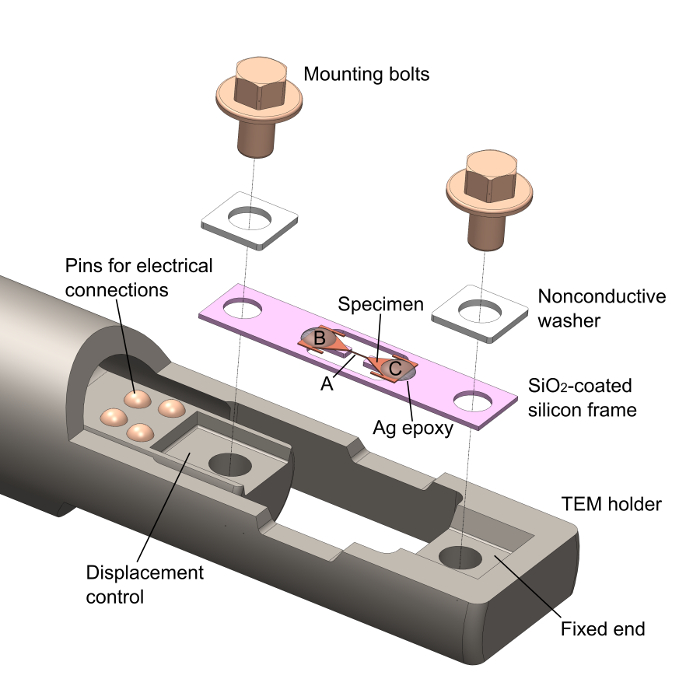
Figure 1: The microdevice-based electromechanical testing system (MEMTS). This image is a three-dimensional (3D) schematic showing the important components and how specimens fit into the TEM holder. Only the wires connecting the specimen to the pins on the TEM holder are not shown. Please click here to view a larger version of this figure.

Figure 2: Silicon frame fabrication process. A bare Si wafer (a) is spin-coated with photoresist (b), which is then patterned using photolithography. The exposed photoresist is developed away to expose the underlying Si wafer (c). The wafer is temporarily bonded to a thicker support wafer and reactive ion etching (RIE) is used to etch through the thinner top wafer (d-e). Acetone is used to remove the photoresist and to detach the support wafer (f). A silicon oxide layer is then deposited on all surface of the etched wafer (g). Finally, individual frames are separated from the wafer by carefully pulling them free of their support tabs (h). Please click here to view a larger version of this figure.

Figure 3: Metallic specimen fabrication. Optical images of (a) an array of copper specimens (b) an individual specimen, and (c) zoom-in view of a gauge section. Fabrication process steps are shown in (d), which is a cross-section along A---A in (b). Both sides of a thin foil are coated with photoresist to protect the sample during laser cutting (d, top). Structures are laser machined (d, second) and then etched to produce smooth edges (d, third). Many specimens can be produced from a single fabrication run as shown in (a). Finally, the photoresist is stripped and individual specimens are gently removed from the specimen sheet (d, bottom). Please click here to view a larger version of this figure.

Figure 4: Focused ion beam (FIB) milling images. Image (a) shows the specimen attached to the Si frame and a close-up view (inset) of the specimen support after it was laser-cut. Images (b)-(e) show the gauge section becoming progressively thinner during successive FIB passes. Each pass removes less material to improve surface finish and decrease material property changes due to the milling process. However, it is possible for gauge section defects to remain (f), which can result in material failure even before any strain is applied (g). Please click here to view a larger version of this figure.

Figure 5: Specimen mounted in a TEM holder. (a) and (b) show an assembled specimen in a TEM holder and final dimension of the gauge section with smooth surfaces using gentle FIB milling. Once the specimen is bonded to the Si frame and silver wires are attached using conductive epoxy (c), the two circular holes in the Si frame are used to mount the specimen in the TEM holder. Nonconductive washers are used to insulate the specimen from the TEM holder. Finally, the silver wires are attached to the TEM holder pins using conductive epoxy. Modified13, with the permission of AIP Publishing. Please click here to view a larger version of this figure.

Figure 6: A representative Single crystal copper (SSC) specimen. (a) shows the gauge section (location A from Figure 1) taken after failure of the gauge section. (b) is a bright field image of the gauge section showing plane dislocations. (c) shows the diffraction pattern at the gauge section. Modified13, with the permission of AIP Publishing. Please click here to view a larger version of this figure.

Figure 7: In situ EAD experimental TEM images. These images reveal mechanical and electrical loading effects on the dislocation motion. (b1)-(b4) show the zoom-in view of Area (b) in (a). (b1) shows the specimen in a post-yield equilibrium state. (b2) identifies dislocation loop formation resulting from additional strain beyond the state shown in (b1). No changes were observed when current was applied (b3). Once strain was increased again, further dislocation changes were again noticed (b4). Reprinted13, with the permission of AIP Publishing. Please click here to view a larger version of this figure.
Discussion
Loading...
$$\rightleftharpoonup{xx}$$
$$\longleftharp{xx}$$,
$$\longrightharp{xx}$$,
Micro/nanotechnology has offered powerful tools to characterize material behavior in analytical chambers including scanning16,18,19,20,21 and transmission electron microscopes13,22,23,24. Such in situ testing capability is highly attractive to the materials science and engineering community, as fundamental microstructures and underlying deformation mechanisms can be directly observed utilizing high resolution electron microscopy25,26.
Here we have presented a microdevice-based method to investigate coupled electrical and mechanical behavior of material samples utilizing unique advantages of in situ TEM. The steps in this approach require average experience using photolithography, reactive ion etching equipment, electron microscopes, and access to and training on a high-quality laser machining system such as the one used here. Although assembly of specimens and silicon holders is accomplished using simple means: silver epoxy and a basic light microscope, care must be taken so as to not damage the specimen gauge section. This is true at all times when handling the specimen. Care must also be taken during the final FIB milling processes of copper specimens. Reducing accelerating voltage (5 kV) and current (<80 pA)27 during the final polishing will reduce possible specimen damage28 and produce a smooth, defect-free gauge section. Another important item to remember is to check that the specimen in electrically isolated from the TEM holder to ensure that the applied current passes through the gauge section once the experiment begins.
The wafer etching process includes some steps that are critical to fabricate a good frame for the EAD specimen. Temporarily bonding the 500 µm supporting wafer to the 180 µm wafer with a uniform temporary adhesive coating between the wafers is important, not only to aid in handling the fragile etched wafer, but the support wafer also facilitates heat transfer during the plasma etching process. Insufficient heat transfer may result in etching of the PR mask and subsequent non-target etching of the silicon frame. It is also important to periodically measure etched trench depth. The thinner top silicon wafer must be completely etched through but there should be minimal etching to the support wafer so that it can act as a uniform heat sink to the thinner wafer. Finally, it is important to thoroughly clean the etched wafer with acetone followed by DI water rinse prior to SiO2 deposition to minimize any remaining residues.
The EAD experimental images shown here are representative of what can be expected but modifications can be made to resolution, dosage, and the frame rate to allow better observation and quantification of dislocations. Also, image processing software can be utilized to analyze a series of TEM images with enhanced resolution.
The MEMTS offers several unique advantages for studying electromechanical material behavior. This system enables direct observation of nanoscale phenomena that govern macroscale material deformations under electromechanical loading. Secondly, the specimen gauge sections with small cross-section provides the ability to apply substantial electric current densities using a low current magnitude, thereby removing safety concerns inherent with using high power instruments. For example, applying a current density of 1,000 A/mm2 to a 1 mm2 gauge section would require 1 kA compared to only 1 mA if the gauge cross-section were reduced to 1 µm2. More importantly, using a lower current aids in thermal management. The MEMTS is also unique in that its alignment and assembly do not require expensive equipment and are not time-intensive compared to other microdevice-based assembly methods.
The method described here lends itself well to electromechanical testing of metals, ceramics, and polymers, but it also can be used to explore the microstructure-dependent electromechanical behavior within each of those material classes. For example, the impact of single- and poly-crystallinity, grain orientation, grain size, phase distribution, and defect density on electromechanical behavior could be investigated by preparing representative samples. Insights gained from such a comprehensive study could provide the understanding needed to further understand the EAD driving mechanism(s) and advance EAD manufacturing capabilities. Speaking more broadly, the MEMTS might be a useful platform for studying other devices which utilize a thermoelectric coupling. For example, it could be used to observe materials used in thermoelectric coolers, which convert an applied voltage to a temperature difference via the Seebeck effect.
Although experiments performed using the process outlined here have yet to show electrically assisted deformation occurs in the absence of significant Joule heating, further experiments are needed. The process described here utilized a small set of experimental conditions and focused on a localized region. A more comprehensive set of experiments using multiple materials, current densities, and time scales is needed to more conclusively verify the existence or absence of purely electrical effects in EAD. One technical limitation of the current MEMTS approach is lack of a capability to quantify force acting on a specimen during in situ experiments. The force measure is essential to obtain stress-strain data (e.g. to quantitatively identify when the specimen has reached flow stress) and, when combined with in situ observations, directly provides microstructure-property relations. Towards this unique research opportunity, we are currently working on modifying Si frames to incorporate integrated force sensors.
Disclosures
Loading...
$$\rightleftharpoonup{xx}$$
$$\longleftharp{xx}$$,
$$\longrightharp{xx}$$,
The authors declare that they have no competing financial interests.
Acknowledgements
Loading...
$$\rightleftharpoonup{xx}$$
$$\longleftharp{xx}$$,
$$\longrightharp{xx}$$,
This work was supported by the ASEE-NRL postdoctoral fellowship and the Office of Naval Research through the US Naval Research Laboratory's Basic Research Program. The authors thank C. Kindle at NRL for his technical support.
Materials
| Name | Company | Catalog Number | Comments |
|---|---|---|---|
| Silicon wafers | Any high-quality polished wafers of the correct thickness will work | ||
| Photoresist | Dow | SR220-7 | |
| Photoresist developer | Shipley | MF 24A | |
| Photoresist developer | Rohm and Haas | MF 319 | |
| Temporary wafer adhesive | Crystalbond 509 | Available from a variety of sources | |
| Iductively Coupled Plasma Reactive Ion Etching (CP-RIE) system | Oxford | Plasmalab system 100 ICP RIE | |
| Profilometer | Veeco | Dektak 150 | |
| Plasma-Enhanced Chemical Vapor Deposition (PECVD) system | Oxford | Plasmalab system 100 PECVD | |
| Thin specimen sheet | Surepure Chemetals | 3702, 3703, 3704 or 2236 | 13 µm and 25 µm-thick copper, 99.99% 4N Pure |
| Photoresist | Shipley | 1818 | |
| 355 nm, 10 W, solid-state, frequency tripled Nd:YVO4 pulsed laser | JDSU | Q301-HD | |
| Liquid ferric chloride | Sigma-Aldrich | 157740 | |
| Conductive silver epoxy | Chemtronics | CW2400 | |
| Silver wires | Any highly conductive metallic wires will work (<100 µm in diameter) | ||
| Focused Ion Beam (FIB) | FEI | Nova 600 | |
| Single tilt straining TEM holder | Gatan | 654 | |
| Displacement controller | Gatan | 902 Accutroller | May be sold with the TEM holder |
| CO2 laser cutter | Universal Laser Systems | VLS 3.50 | Use 50% power and 15% speed |
| Electrical insulation sheet | 0.5 mm-thick Hard Fiber Electrical Grade Sheet (Fishpaper) | Available from a variety of sources | |
| Transmission Electron Microscope (TEM) | FEI | Tecnai G2 | |
| External power supply | Keithley | 2400 SourceMeter |
References
Loading...
$$\rightleftharpoonup{xx}$$
$$\longleftharp{xx}$$,
$$\longrightharp{xx}$$,
- Ross, C. D., Kronenberger, T. J., Roth, J. T. Effect of dc on the formability of Ti-6Al-4V. J Eng Mater-T ASME. 131 (3), 031004(2009).
- Siopis, M. S., Kinsey, B. L. Experimental investigation of grain and specimen size effects during electrical-assisted forming. J Manuf Sci Eng-T ASME. 132 (2), 021004(2010).
- Green, C. R., McNeal, T. A., Roth, J. T. Springback Elimination for Al-6111 Alloys Using Electrically Assisted Manufacturing (EAM). 37th Annual North American Manufacturing Research Conference. 37, Greenville, SC. 403-410 (2009).
- Okazaki, K., Kagawa, M., Conrad, H. A study of the electroplastic effect in metals. Scr Mater. 12 (11), 1063-1068 (1978).
- Sprecher, A. F., Mannan, S. L., Conrad, H. Overview no. 49. On the mechanisms for the electroplastic effect in metals. Acta Metall. 34 (7), 1145-1162 (1986).
- Perkins, T. A., Kronenberger, T. J., Roth, J. T. Metallic forging using electrical flow as an alternative to warm/hot working. J Manuf Sci Eng-T ASME. 129 (1), 84-94 (2007).
- Andrawes, J. S., Kronenberger, T. J., Perkins, T. A., Roth, J. T., Warley, R. L. Effects of DC current on the mechanical behavior of AlMg1SiCu. Mater Manuf Process. 22 (1), 91-101 (2007).
- Dzialo, C. M., Siopis, M. S., Kinsey, B. L., Weinmann, K. J. Effect of current density and zinc content during electrical-assisted forming of copper alloys. CIRP Ann Manuf Techn. 59 (1), 299-302 (2010).
- Fan, R., Magargee, J., Hu, P., Cao, J. Influence of grain size and grain boundaries on the thermal and mechanical behavior of 70/30 brass under electrically-assisted deformation. Mater Sci Eng A. 574, 218-225 (2013).
- Magargee, J., Morestin, F., Cao, J. Characterization of Flow Stress for Commercially Pure Titanium Subjected to Electrically Assisted Deformation. J Eng Mater Technol. 135 (4), 041003(2013).
- Kinsey, B., Cullen, G., Jordan, A., Mates, S. Investigation of electroplastic effect at high deformation rates for 304SS and Ti-6Al-4V. CIRP Ann - Manuf Technol. 62 (1), 279-282 (2013).
- Williams, D. B., Carter, C. B. Transmission electron microscopy. , 2nd edn, Springer. (2008).
- Kang, W., Beniam, I., Qidwai, S. M. In situ electron microscopy studies of electromechanical behavior in metals at the nanoscale using a novel microdevice-based system. Rev Sci Instrum. 87 (9), (2016).
- Kim, M. J., et al. Electric current-induced annealing during uniaxial tension of aluminum alloy. Scr Mater. 75, 58-61 (2014).
- Knowles, M. R. H., Rutterford, G., Karnakis, D., Ferguson, A. Micro-machining of metals, ceramics and polymers using nanosecond lasers. Int J Adv Manuf Tech. 33 (1-2), 95-102 (2007).
- Kang, W., Saif, M. T. A. A novel SiC MEMS apparatus for in situ uniaxial testing of micro/nanomaterials at high temperature. J Micromech Microeng. 21 (10), (2011).
- Callister, W. D. Materials Science and Engineering: An Introduction. , 7th edn, John Wiley & Sons, Inc. (2007).
- Kang, W., Saif, M. T. A. A Novel Method for In Situ Uniaxial Tests at the Micro/Nano Scale-Part I: Theory. J Microelectromech Syst. 19 (6), 1309-1321 (2010).
- Kang, W., Han, J. H., Saif, M. T. A. A Novel Method for In Situ Uniaxial Tests at the Micro/Nanoscale-Part II: Experiment. J Microelectromech Syst. 19 (6), 1322-1330 (2010).
- Kang, W. M., Saif, M. T. A. In Situ Study of Size and Temperature Dependent Brittle-to-Ductile Transition in Single Crystal Silicon. Adv Func Mater. 23 (6), 713-719 (2013).
- Sim, G. D., Vlassak, J. J. High-temperature tensile behavior of freestanding Au thin films. Scr Mater. 75, 34-37 (2014).
- Haque, M. A., Saif, M. T. A. Deformation mechanisms in free-standing nanoscale thin films: A quantitative in situ transmission electron microscope study. Proc Natl Acad Sci U S A. 101 (17), 6335-6340 (2004).
- Zhu, Y., Espinosa, H. D. An electromechanical material testing system for in situ electron microscopy and applications. Proc Natl Acad Sci U S A. 102 (41), 14503-14508 (2005).
- Hosseinian, E., Pierron, O. N. Quantitative in situ TEM tensile fatigue testing on nanocrystalline metallic ultrathin films. Nanoscale. 5 (24), 12532-12541 (2013).
- Kang, W., Rajagopalan, J., Saif, M. T. A. In Situ Uniaxial Mechanical Testing of Small Scale Materials-A Review. Nanosci Nanotechnol Lett. 2 (4), 282-287 (2010).
- Kang, W., Merrill, M., Wheeler, J. M. In Situ Thermomechanical Testing Methods for Micro/Nano-Scale Materials. Nanoscale. , (2016).
- Thompson, K., Gorman, B., Larson, D., Bv Leer,, Hong, L. Minimization of Ga Induced FIB Damage Using Low Energy Clean-up. Microsc Microanal. 12 (S02), 1736-1737 (2006).
- Mayer, J., Giannuzzi, L. A., Kamino, T., Michael, J. TEM sample preparation and FIB-induced damage. MRS Bulletin. 32 (5), 400-407 (2007).
Reprints and Permissions
Request permission to reuse the text or figures of this JoVE article
Request Permission