Volume is an important parameter regarding physiological and pathological characteristics of cells. We describe a fluorescent exclusion method allowing full-field measurement of in vitro neuronal volume with sub-micrometric axial resolution required for the analysis of neurites and dynamic structures implied in neuronal growth.
Method Article
High-resolution Volume Imaging of Neurons by the Use of Fluorescence eXclusion Method and Dedicated Microfluidic Devices
In This Article
Summary
Abstract
Volume is an important parameter regarding physiological and pathological characteristics of neurons at different time scales. Neurons are quite unique cells regarding their extended ramified morphologies and consequently raise several methodological challenges for volume measurement. In the particular case of in vitro neuronal growth, the chosen methodology should include sub-micrometric axial resolution combined with full-field observation on time scales from minutes to hours or days. Unlike other methods like cell shape reconstruction using confocal imaging, electrically-based measurements or Atomic Force Microscopy, the recently developed Fluorescence eXclusion method (FXm) has the potential to fulfill these challenges. However, although being simple in its principle, implementation of a high-resolution FXm for neurons requires multiple adjustments and a dedicated methodology. We present here a method based on the combination of fluorescence exclusion, low-roughness multi-compartments microfluidic devices, and finally micropatterning to achieve in vitro measurements of local neuronal volume. The high resolution provided by the device allowed us to measure the local volume of neuronal processes (neurites) and the volume of some specific structures involved in neuronal growth, such as growth cones (GCs).
Introduction
The precise knowledge of cellular volume has attracted increased attention in the last years, driven by the issue of cell size homeostasis in single-celled microorganisms 1 and more generally in mitotic cells 2. However, the question of cell volume is pertinent also for post-mitotic cells, for which neurons constitute a paradigmatic example.
Volume is indeed an important signature of physiological and pathological events at different scales and time-points in neuronal life, from transient axonal deformation associated to electrical activity (millisecond scale) 3 to the irreversible neuronal swelling occurring during the asymptomatic phase of neurodegenerative diseases (over years in humans) 4. However, the largest volume change occurs in an intermediate time scale of days or weeks (depending on the considered organism) during neuronal growth. The extended and complex morphology of neurons raises multiples issues, among which the regulation of cell size. Axonal length and diameter are indeed tightly regulated in vivo, with values specific to each neuronal type 5,6.
These issues, complex to address in vivo, can also be addressed in a simplified way in vitro. In that aim, a method dedicated to volume measurement fast enough to follow growth dynamics (i.e. in a time scale of minutes) and compatible with observation over hours or days is required. Several methods have been developed over the years to provide a direct or indirect access to cellular volume in vitro. Cell reconstruction from confocal imaging is one of them, but this method implies labeling and repeated exposures to light while showing a limited axial resolution of about 500 nm 7. Note that these two last drawbacks are partially overcome by a more sophisticated and recent method named lattice light-sheet microscopy 8. Atomic Force Microscopy has been used 9 but this scanning method is by essence slow and tedious. Moreover, the physical contact it requires with the cell might interfere with the measurement considering the extreme softness of neurons 10. Indirect method using impedance or resonance have been employed for different cell types 11, but are inadequate for extended adhesive cells like neurons.
One of the most promising methods is based on the measure of the excluded volume of cells in a close chamber filled with a fluorescent dye. The Fluorescence eXclusion method (FXm) is simple in its principle as it requires no labeling, and is suitable for fast, long term optical imaging of cell populations with a potentially sub-optical axial resolution. More precisely, the resolution in z depends on the maximum fluorescence intensity in the culture chamber (i.e. in region devoid of cells) divided by the dynamic range of the camera, although several sources of noise limit this ultimate resolution. This method has been very powerful to follow the volume of migrating adherent cells 12 or to study volume change during mitosis of mammalian cells, as thoroughly described in 13. However, neurons constitute a methodological challenge for FXm considering their extensive ramification into sub-micrometric processes.
We present here a method leading to the fabrication of smooth FXm chambers to access with high precision the volume and height of neuronal branches and dynamic structures involved in neuronal growth like growth cones.
Chambers should have similar heights than the object to measure in order to optimize axial resolution. Therefore, we designed different FXm devices characterized by central measurement chambers of three different heights. The thinnest (3 µm in height) is dedicated to neurite measurement: this low height excludes soma, which remain in the near 15 µm high intermediate chamber. Thicker central chambers (10 and 12 µm) are sufficiently high to follow the whole cell growth. The device also includes two reservoirs located on either side of the central chamber. Four injection holes (IH) are thus implemented and are designated as follows: the inlet and outlet serve to introduce the cellular suspensions into the chip, whereas the two others feed the reservoirs.
We have first fabricated calibration coverslips for height measurements using photoresist structures of known geometry. We have then imaged free growing neurons, but also morphologically constrained neurons into micropatterns of adhesion.
Protocol
The study was carried out in accordance with European Community guidelines on the care and use of laboratory animals: 86/609/EEC. The research purpose and the protocol are described in the Ethical Annex of ERCadg project CellO, which was approved and is regularly reviewed by the ERCEA. Institut Curie animal facility has received licence #C75-05-18, 24/04/2012, reporting to Comité d'Ethique en matière d'expérimentation animale Paris Centre et Sud (National registration number: #59).
1. Fabrication of the mold
NOTE: The mold includes central and intermediate chambers connected to an inlet and an outlet, plus two reservoirs (and inlets) located on both sides of the central chamber.
- Use flat tweezers to manipulate 51 mm diameter silicon wafers and transfer them from one place to another.
- Central chamber silicon mold
- Fill a 2-mL plastic pipette with positive photoresist. Position the pipette at the center of a 51-mm diameter silicon wafer and press on its reservoir until covering about 75% of the wafer surface with the photoresist. Spin-coat at 3000 rpm for 30 s.
- Transfer the wafer from the spin-coater to a hotplate, with a surface temperature of 100 °C, for 50 s.
- Transfer the wafer from the hotplate to the substrate holder (chuck) of the mask aligner. Expose through the "DRIE mask" (see Supplementary files "masks_neuron_volume_chips.tiff" and "masks_neuron_volume_chips.dxf").
- Remove the wafer from the chuck then dive it in a 100-mL glass crystallizing dish containing the developer (dilution 1:4 in deionized water). Release the wafer and maintain it for 1 min while continuously and gently stirring the crystallizing dish.
NOTE: To save reagents, fill the crystallizing dish to 1 cm in height at maximum. - Take back the wafer from the developer and submerge it into a 100-mL crystallizing dish filled with deionized water for about 10 s.Then place the wafer on an absorbent paper and dry it with pressurized nitrogen using an air blow gun.
- Place the wafer for 50 s on a hotplate with a surface temperature of 115 °C.
- Perform deep-Reactive Ion Etching (DRIE) with the following parameters (more information on the DRIE technique can be found in references 14 and 15); Passivation step: 50 sccm of C4F8, He backing flow 10 sccm, CP 10 W, Inductively Coupled Plasma (ICP) 1500 W, total pressure 24 mbar, temperature 18 °C; Etching step: 100 sccm of SF6, He backing flow 10 sccm, CP 11 W, ICP 1500 W, total pressure 24 mbar, temperature 18 °C; Passivation time: 4 s; Etching time: 7 s; Total process duration: typically 5 min for about 10 µm etched depth.
- Dissolve the photoresist by diving the substrate into a crystallizing dish filled with acetone.
- Submerge the wafer in a piranha solution (2/3 of H2O2 (30%) and 1/3 of H2SO4 (95%)) for 5 min.
Caution: Always add H2O2 first and then H2SO4 and rinse at least 3 times in deionized water after cleaning.
- Fabricate the molds corresponding to intermediate chambers by performing steps 1.2.1 to 1.2.11 following the parameters listed in Tables 1-3.
NOTE: Each table corresponds to a given device characterized by a specific height of the central observation chamber.
NOTE: Perform the whole process using increasing photoresists heights (Masks 1 to 3 for each device, see Supplementary files "masks_neuron_volume_chips.tiff" and "masks_neuron_volume_chips.dxf").- Place the etched silicon wafer on the spin-coater substrate holder.
- Check that the spin-coater is working properly by verifying that the aspiration of the substrate is effective (the substrate should spin and stay in place during the nominal rotation speed).
- The viscosity of SU-8 increases with the height of the targeted thickness range. Always use 20-30 mL bottles to store SU-8 photoresists and pour it on the wafer before spin-coating (SU-8 might be too viscous to be manipulated with a plastic pipette).
- Pour negative epoxy-type photoresist SU-8 at the center of the substrate until covering about 75% of the silicon wafer, then spin-coat using the parameters indicated in row "Spincoating" of the Tables.
- Place the coated wafer on a hotplate for the duration and temperature indicated in row "Soft bake".
- Mount the etched wafer and the adequate "SU-8 Mask" on the mask aligner.
- Align the etched wafer with the mask using the dedicated alignment crosses (typical size of these crosses: 50 µm × 150 µm) designed on each mask.
NOTE: Two crosses on each side of the device are sufficient (one at the bottom left and one at the top right). - Expose using the I-line of the mask aligner (wavelength 365 nm) with the appropriate UV dose, as indicated in row "Exposure energy".
NOTE: The exposure time is calculated by dividing the exposure energy E specific for each photoresist by the effective power of the UV lamp, modulated by the absorption of the mask: x (1- Absorptionmask). Absorption is about 20% for flexible masks and negligible for chromium hard mask.
 - Place the coated wafer on a hotplate for the duration and temperature indicated in row "Post bake".
- Prepare two 100-mL glass-crystallizing dishes, one containing the developer, the other empty. Dive the wafer in the developer for the duration indicated in row "Development". Agitate gently the crystallizing dish all along development
- Sprinkle the wafer with isopropanol above the empty crystallizing dish for about 5 s. Finally, place the wafer on an absorbent paper and dry it with pressurized nitrogen using an air blow gun.
- Place the coated wafer on a hotplate for the duration and temperature indicated in row "Hard bake" (optional).
NOTE: This step is useful to avoid cracks in the photoresist and provide a homogeneous flat surface for the next steps. - Repeat steps 1.3.1 - 1.3.10 to complete the processes listed in Table 1-3.
- After the last step of photolithography, silanize the final master mold consisting of 3 layers of negative photoresists by dispatching two 100 µL droplets of Trichloro(1H,1H,2H,2H-perfluoro-octyl) silane on each side of the master in a 100-mm Petri dish. Seal the Petri disk with a plastic paraffin film and incubate 20 min at room temperature (RT).
NOTE: The master mold is ready and can be used several times.
- Place the etched silicon wafer on the spin-coater substrate holder.
2. Fabrication of PDMS chip
- Pour 90 g of silicon-based organic polymer (Polydimethylsiloxane: PDMS) into a 100-mL plastic cup. Add 10 g of its curing agent (1:10 in weight). Stir the mixture using a plastic pipette for 2-3 min.
NOTE: Mix 90 g of PDMS with 10 g of curing agent for the fabrication of 6 chips. - Place the mixture within a vacuum desiccator and pump for about 30 min to remove air bubbles trapped into the PDMS.
- Place the master mold in a P100 Petri dish and pour 15 mL of the mixture on the mold using a syringe.
NOTE: 15 mL leads to a total chip height of 1.5 mm. - Place the PDMS-mold structure within a vacuum desiccator and pump until there are no more air bubbles bursting at the surface of the PDMS.
NOTE: This step takes about 30 min. - Push the wafer at the bottom of the Petri dish using a cone tip to avoid dead PDMS volume below the wafer. Place the PDMS-mold device in the oven set at 70 °C for at least 2 h.
- Demold the PDMS block under a chemical hood using a stainless steel flat spatula and by pouring isopropanol on the chip. Place it on the stainless steel bench of the hood.
- Cut around the silicon wafer and demold the PDMS replica using a scalpel.
- Cut around (leave a 2-mm margin) the chip using a scalpel or a razor blade.
- Punch inlets by pressing the 1.5 mm diameter puncher firmly and actuate it to cut and carve the hole of the inlet. Do the same at the four dedicated zones of the chip where liquid will be injected.
- Clean the chip by sticking and peeling adhesive tape on the microstructured side. Sprinkle isopropanol on both sides. Then dry the chip with pressurized nitrogen using an air blow gun.
3. Fabrication of patterned coverslips (24 × 24 mm2)
NOTE: Manipulate coverslips with curved tweezers.
- Poly-ornithine (PLO) patterns
- Apply an O2 cleaning plasma on glass coverslips. Plasma parameters: pumping down pressure: 0.25 mbar; O2 supply duration: 3 min; gas flow: 10 sccm; maximum deviation: ±5 sccm; plasma duration: 3 min; set pressure: 0.36 mbar; maximum deviation: ±0.10 mbar; set power: 50 W; maximum deviation: 5%; venting duration: 45 s.
- Mix 484 µL of acetic acid and 56 µL of 3-methacryloxypropyl-trimethoxysilane, complete with absolute ethanol to get a total volume of 15 mL.
- Using a 1-mL tip cone, put a drop of 500 µL of this solution on each coverslip, wait for 2-3 min. Dry using a cleanroom microfiber wiper.
NOTE: Silanized glass coverslips can be stored up to 1 month at room temperature within plastic boxes sealed with a plastic paraffin film. - Place each coverslip on a spin coater located in a clean room environment. Put a drop of a positive photoresist covering about 75% of the coverslip (about 500 µL) and spin-coat at 4000 rpm for 30 s to reach a final thickness of 0.45 µm.
- Place the coverslips for 1 min on a hotplate with a surface temperature of 115 °C.
- Using a mask aligner, expose each coverslip at a wavelength of 435 nm (G-line) through the dedicated mask according to the fabricant parameters (UV dose about 50-60 mJ.cm-1)
- Prepare 2 glass crystallizing dishes, one containing the developer (no dilution), the other containing deionized water.
- Dive one by one each coverslip in the developer for 1 min while continuously and gently stirring the crystallizing dish. Then submerge the wafer in deionized water for about 5 s. Place the wafer on an absorbent paper and dry it with pressurized nitrogen using an air blow gun.
- Apply an activation O2 plasma with the same parameters as in 3.1.1.
- Under the hood, depose four 170 µL drops of a 100 µg/mL PLO solution per P100 Petri dish. Put the patterned face of the coverslips on each of these drops. Seal the Petri dish with a plastic paraffin film to avoid drying. Incubate overnight at RT.
NOTE: The PLO solution should remain attached to the coverslips by capillarity. - Prepare four recipients (typically P60 Petri dishes), fill three of them with PBS and the fourth one with deionized water. Prepare two glass crystallizing dishes of pure ethanol.
- Take out each coverslip from the Petri dishes, submerge it in the first PBS bath for 10-15 s, evacuate the liquid on an absorbing tissue by putting the coverslip vertically on the side, insert it with e.g. the patterned face up inside the ethanol bath.
NOTE: Once the dissolution of the photoresist is completed, it becomes difficult to locate the patterned side of the coverslip. Therefore, it is important at this stage to trace its location. - Place the ethanol crystallizing dish within an ultrasonic bath sonicator (120 W / 35 kHz) and let the photoresist be dissolved for 3 min.
NOTE: Change the ethanol bath every 4 coverslips to limit dilution by the PBS that might impair the dissolution of the photoresist. - Take out the coverslip from the ethanol bath, then dive it several times into the second PBS bath. Check the surface aspect repeatedly until the greasy-like surface that results from the remaining liquid film of ethanol disappears.
- Submerge for 5-10 s the coverslip into the third PBS bath. Then immediately transfer it to the deionized water bath. Place the coverslip on an absorbent paper and dry it with pressurized nitrogen using an air blow gun.
NOTE: The last rinse in deionized water is used to avoid the formation of PBS crystals during the drying step.
- Photoresist structures for height calibration
- Perform only steps 3.1.4. to 3.1.8. using the dedicated mask (mask "Photoresist stripes", see Supplementary file "Mask_Photoresist-stripes.dxf").
4. Chip assembling and final implementation
- Chip assembling on glass bottom dishes
- Put both the PDMS chip and the glass dish on which it will be bonded into the plasma chamber for surface activation. Parameters: pumping down pressure: 0.25 mbar; O2 supply duration: 3 min; gas flow: 10 sccm; maximum deviation: ±5 sccm; plasma duration: 30 s; set pressure: 0.40 mbar; maximum deviation: ±0.10 mbar; set power: 50 W; maximum deviation: 5%; venting duration: 45 s.
- Gently put the activated PDMS chip in contact with the glass coverslip, and delicately apply pressure on the edges of the chip to bond the chip to the coverslip. To increase the bonding strength, place the device in the oven at 70 °C for 5 to 10 min.
NOTE: Do not press on parts containing pillars, they might collapse under too much pressure. - Under the hood (i.e. at RT) and within 30 min after bonding, place a 10-µL tip cone filled with a 100 µg/mL PLO solution at the IHs, then inject the liquid. Adjust the volume in order to form a drop at the top of each IHs. Then, using a 1-mL tip cone, add PBS in the Petri dish all around the chip.
- Let the chip at RT with a minimum of 2 h incubation time. For overnight incubation, seal the Petri dish using a plastic paraffin film to avoid drying.
NOTE: The liquid should not leak outside the chip otherwise the chip must be discarded. - Press a 10-µL tip cone lightly into each IH and suck up the excess of liquid. Then stick completely the tip cone inside the outlet and draw up the remaining liquid.
- Replace PLO by laminin following the instructions given in steps 4.1.5 (emptying) and 4.1.3 (filling). Incubate at RT for 1 h.
- Replace laminin by the culture medium following the instructions given in steps 4.1.5 (emptying) and 4.1.3 (filling). Composition of the culture medium: MEM 81.8%; Sodium Pyruvate 100 mM 1%; Glutamax 200 mM 1%; Horse Serum 5%; B27 supplement 2%, N2 supplement 1%, Gentamicin 0.2%; filter the solution using a 220-nm filter. Using a 1-mL tip cone, replace also the PBS surrounding the chip by this medium.
- Put the chip into the incubator regulated at 37 °C and 5% CO2 for at least 5 h (or overnight) before neuron seeding.
- Chip assembling using patterned coverslips
NOTE: If the patterned coverslips include positive photoresist reference objects, perform steps 4.2.1 to 4.2.9. Otherwise, perform only step 4.2.3, stick the PDMS device on the PLO patterned coverslip as indicated in 4.1.2, put culture medium inside and around the chip then go to step 4.2.10.- Deposit a drop of water on a rectangular thick microscope glass slide and stick the coverslip on the glass slide by capillarity (non-patterned side facing the glass slide). Under a microscope, mark the location of the photoresist stripes at the rear of the glass slide using a felt pen.
- Place the patterned glass coverslip on the mask holder of the mask aligner. Rely on the mark made with the felt pen to center the photoresist reference objects.
- Perform the plasma step as described in 4.1.1 on the PDMS chip.
- Place the PDMS chip on the mobile substrate holder (chuck) of the mask aligner.
NOTE: To increase optic contrast, place a silicon wafer beneath the PDMS chip. The silicon wafer should remain firmly attached on the chuck during the alignment process (use a transparent tape to stick it to the chuck). - Lift the chuck at the limit of mechanical contact to align the chip with the array of photoresist stripes located on the coverslip.
- Achieve mechanical contact between the chip and the coverslip by finishing up lifting the chuck until the surface of the PDMS pillars touch the glass coverslip.
- Lower the chuck. Remove the coverslip now bonded to the chip from the mask holder. Then place the device into a 35-mm Petri dish, and transfer everything into the oven (temperature: 70 °C) for 5 to 10 min to increase the bonding strength.
- Perform as in step 4.1.3.
NOTE: if using PLO patterned coverslips, go directly from step 4.2.7 to step 4.2.9. - Replace PLO by the plating medium following the procedures described in steps 4.1.5 (emptying) and 4.1.3 (filling). Using a 1-mL tip cone, replace also the PBS surrounding the chip by this medium.
- Put the chip into the incubator regulated at 37 °C and 5% CO2 until neuron seeding, with a minimum of 5 h incubation time.
5. Neuron culture
- Prepare 100 mL of dissection medium (HH medium) by mixing 10 mL of HBSS 10x, 2 mL of Hepes 1 M and 88 mL of sterile water in a 200-mL plastic flask.
NOTE: The HH medium can be prepared the day before the culture. - Dissect hippocampus from E18 mice embryo extracted from a mother euthanized by cervical dislocation (C57BL/6J mice from Charles Rivers). Steps of dissection are e.g. detailed in 16.
- Place hippocampus in a plastic tube containing trypsin (0.3 mL of trypsin 2.5%, w/o EDTA into 2.7 mL of HH medium) for 10 min at 37 °C in order to initiate chemical dissociation.
- Discard almost all the liquid and replace it with 5 to 10 mL of HH using disposable plastic pipettes. Do it 3 times. For the last fill, use 1 mL of plating medium instead of HH.
- Mechanically dissociate tissues using a 1 mL tip-cone by aspiring and ejecting the full volume several times, avoiding making bubbles and using no more than 15-20 passages.
- In a separate 500 µL recipient, prepare a solution using 5 µL of cell suspension diluted in 45 µL of PBS. Take 1 µL of this solution using a 10 µL pipette and insert the diluted suspension into a Malassez cell counter. Use the indications provided in 17 to estimate the number of cells.
NOTE: A single hippocampus usually provides about 0.5 million of neurons. - Centrifuge at 100 x g for 6 min at RT.
- Discard the supernatant and replace it by the volume of plating medium required to achieve a concentration of 10 million cells/mL. Resuspend cells by successively aspire and eject the cell suspension with a 1-mL tip cone.
- Draw up the plating medium present in the chip (refer to step 4.1.5). Collect 2-3 µL of the freshly resuspended solution using a 10-µL pipette and inject it at the inlet (refer to the injection procedure described in step 4.1.3). Repeat immediately the same operation at the outlet.
- Inject about the same volume of plating medium in each reservoir (refer to step 4.1.3).
NOTE: Quickly observe the chip under the microscope to check the density of cells. The order of magnitude of the optimal cell density corresponds to about 5-10 cells within the square surface delimited by 4 pillars (about 0.3 mm2, i.e. about 15-20 cells per mm2). - Eventually repeat step 5.10 using instead 0.5-1 µL of cell suspension to reach the targeted cell density.
- Place the seeded chip into an incubator regulated at 37 °C 5% CO2.
6. Fluorescence exclusion observation
- Replacement of culture medium by the imaging medium.
- Prepare the imaging medium as in 4.1.7 but use instead MEM devoid of phenol red and add fluorescent dextran. In that aim, dilute dextran (molecular weight 10,000 g/mol, stock solution concentrated at 10 mg/mL in PBS) in order to achieve a final concentration of 0.5-1 mg/mL in the imaging medium.
NOTE: Use Dextran conjugates with Absorption/Emission maxima 496/524 or 650/668. Prefer the first to image 0.45 µm high positive photoresist structures (to get rid of their auto fluorescence in the red bandwidth) and the second to image neurons (less toxic). - Empty all inlets using a 10-µL pipette and re-fill them completely with the imaging medium (refer to steps 4.1.3 and 4.1.5 for the precise methodology of medium replacement).
- Prepare the imaging medium as in 4.1.7 but use instead MEM devoid of phenol red and add fluorescent dextran. In that aim, dilute dextran (molecular weight 10,000 g/mol, stock solution concentrated at 10 mg/mL in PBS) in order to achieve a final concentration of 0.5-1 mg/mL in the imaging medium.
- Imaging
- Place the chip under an epifluorescence microscope equipped with an environmental chamber regulated at 37 °C and 5% of CO2. Use a 40X, numerical aperture (NA) 0.8 dry objective, 30% of full power (full power: 3 W) and 30 ms of exposure time. Acquire images of cells at focus (from single to multiple successive images in case of time-lapse experiments).
- Image analysis
- Normalize images using the background reduction routine implemented in dedicated software to get a homogeneous background. See 13 for the details of the image processing steps included in this software. The output image has a .MAT format.
- Convert .MAT file into .TIFF 8 bits images using the routine put in supplementary material (conversion_mattotiff.m, which calls for importfilevol.m).
- Perform Import > Image Sequence on ImageJ to build a video from the .TIFF images.
- Compute the mean intensity P of a square area localized in the center of a pillar (reference object) and the mean intensity B of a square area of the chamber devoid of cells (background, i.e. height zero). See 18 for an example of detailed methodology of image processing.
NOTE: The lateral dimension of the square areas used as intensity references must be about half of the pillar diameter to get a sufficient number of pixels while avoiding light pollution from the pillar edges. - Use the P and B values to establish the linear conversion law from intensity i to height h:

with hc the known height of the chamber, and
and 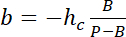
NOTE: PDMS displays no detectable autofluorescence. - Select an area around the zone of interest, integrate intensity using ImageJ (see 19 for more details) and apply the conversion law obtained in 6.3.5 to measure the volume of a cell compartment.
NOTE: The zone of interest might be selected based on the fluorescence of sub-cellular elements like actin, e.g., for the selection of growth cones in GFP-LifeAct neurons, select the zone of interest in the GFP emission channel, save the contour of this zone using a ROI manager tool, then measure the cell volume enclosed within the same zone in the emission channel of dextran (in red).
Results
The result of the process of fabrication described in sections 1 and 2 is illustrated by the images of Figure 1A-1B and the curve of Figure 1C. The table of Figure 1D displays the roughness values of two different representative areas of the PDMS chip, i.e. in the central and the 20 µm high next intermediate chamber. A decrease in roughness by a factor of about 7 has been obtained by using etched Si wafer instead of SU-8 photoresist. Then, FXm was first applied on a photoresist stripe of known geometry (Figure 2A) within a 10 µm high chamber. After image processing and intensity to height conversion (see the graph of Figure 2B), FXm profiles performed on cross-sections along this stripe (Figure 2C) provide the desired height profiles (Figure 2D). Figure 2D shows the comparison between profiles obtained using mechanical profilometry and FXm methods. These profiles, including edge and plateau value, are very similar, validating the method. Note that the scattering of FXm data is not representative of the ultimate resolution of the method, as further assessed in Figure 3 and Figure 4, but results from the low intensity employed to avoid a possible effect of the very weak auto-fluorescence of the photoresist in the GFP channel.
Then, we observed neurites in 3 µm and 10 µm high chambers (Figure 3). The standard deviation of the background noise is about 18 nm after intensity to height conversion and background correction. This value is slightly higher than the physical roughness of PDMS surfaces casted on silicon surfaces (12 nm, see the table of Figure 1D) but much lower than the roughness measured on PDMS obtained from SU-8 molds. These results highlight the added value of drilling wells into silicon wafers rather than opening holes into SU-8 photoresist to cast pillars. Such a low value allows a high signal to noise ratio and very clear images in volume such as the one displayed in Figure 3A. As an example of the data that can be retrieved from such images, we computed the volume of 1.6 µm (i.e. 10 pixels) wide neurite slice (see the graph of Figure 3B). Using in a first approximation a linear fit of these data gives a mean neurite height value of about 400 nm, to be compared with e.g. the 500-nm axonal diameter found in 10 days old pups within the corpus callosum 5. We also combined FXm with micropatterns of adhesion consisting of serially abutted 2 µm and 6 µm wide stripes of 30 µm in length. Our aim was to study the influence of the neurite width on its 3D shape. Figure 3C shows a 3D representation in false color of a whole neuron image obtained in a 10 µm high chamber. Neurites are spreading on 2 µm and 6 µm wide stripes, whereas the soma is located on the extremity of the largest stripe. Height profiles were drawn in three different cross sections. In coherence with the graph displayed in Figure 3A, the surface integrated over the cross-sections increase with the neurite width (Figure 3D).
We also focused on growth cone (GC) 3D structures. Figure 4A-B displays two different GC profiles obtained in a 3 µm high chamber, which highlight their branched sub-structure. In addition, we performed time-lapse experiments to follow the dynamics of the volume of GCs in a 12 µm high chamber. Figure 4C displays a cycle of shrinking and reactivation of a given GC within a time scale of a few tens of minutes. Thanks to the use of GFP-lifeact mice, growth cones were localized in the GFP emission wavelength (510 nm) from their high actin concentration. The surface identified at the wavelength was used to integrate over the dextran emission wavelength at 647 nm to compute GC volume. Figure 4D shows finally the distribution of GC volume at different time points and location on three different neurons, centered on a value of about 6 µm3.
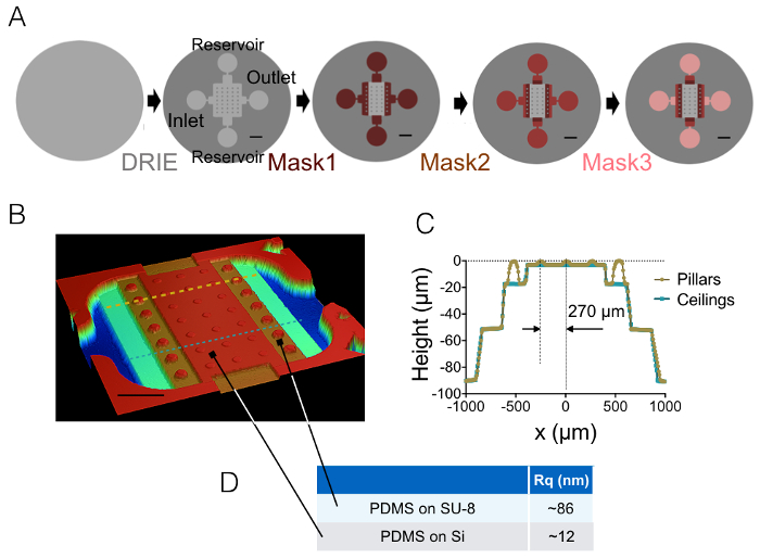
Figure 1: FXm PDMS chambers. (A) Schemes of the four different main steps of microfabrication leading to the final mold. The location of the inlet, outlet and reservoirs are indicated. Scale bars: 1 mm. (B) Image of the PDMS FXm chamber obtained using an optical profilometer. This image shows the central chamber containing 3 rows of 10 µm high pillars and the intermediate chambers of 20, 50 and 90 µm in height. Scale bar: 500 µm. (C) Cross-sectional view of the chip along the two dashed lines drawn in (B). Yellow/gold: cross-section along pillars, blue: cross-section between pillars. (D) Mean values of the PDMS roughness measured on 50 × 50 µm2 areas molded on silicon and on the 20 µm high SU-8 intermediate chamber (see arrows for the location of these areas). Mean values were obtained from the measurements of three different areas. Please click here to view a larger version of this figure.
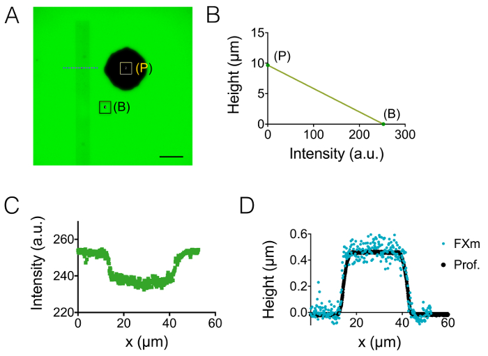
Figure 2: Calibration of FXm method using a photoresist stripe as the object of interest. (A) GFP-fluorescence image taken in a 10 µm high chamber filled with 10,000 MW dextran absorbing at 488 nm at 1 mg/mL. (B: background, P: pillar). Observation with a dry 40X NA 0.8 objective. Scale bar: 50 µm. (B) Linear calibration law obtained from the mean intensity of the two colored rectangles shown in A. (C) Fluorescence intensity profile obtained at the level of the blue dashed line displayed in (A), crossing the photoresist stripe (0.45 µm high positive photoresist). (D) Comparison of the profiles obtained from mechanical profilometer (black dots) and FXm after intensity to height conversion of the data of (B) (blue dots). Please click here to view a larger version of this figure.
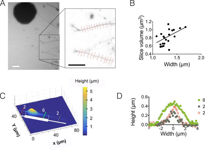
Figure 3: Neurite volume imaging. (A) Neurite extending into the central 3 µm high chamber from soma located in the next 15 µm intermediate chamber. Imaging performed using 10,000 MW dextran absorbing at 488 nm and a 40X, NA 0.8 dry objective. The inset obtained after the use of the background reduction routine highlights the two neurites and chosen to plot the graph on the right. Scale bars: 30 µm. (B) Neurite slice volume as a function of neurite width obtained from the 22 profiles (average on 10 pixels, i.e. on a 1.6 µm "neurite slice") shown in (A). The solid line represents a linear fit of slope 0.4 µm passing through the origin. (C) False color image of a patterned neuron on an adhesive stripe made of successive 2 µm and 6 µm wide stumps (represented in white). Measurements were made in a 10 µm high chamber filled with 10,000 MW dextran absorbing at 647 nm and using a 40x NA 0.8 dry objective. (D) Height profiles corresponding to the colored dashed lines shown in (C), keeping the same color code. Please click here to view a larger version of this figure.
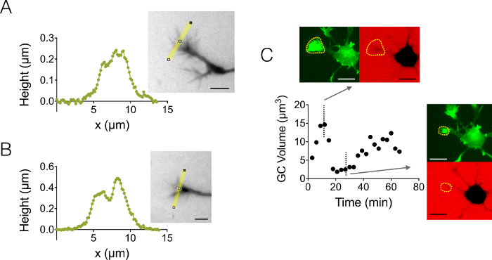
Figure 4: Static and dynamic growth cone imaging. (A-B) Growth cone height profiles obtained in a 3 µm high chamber after intensity to height conversion along the yellow lines displayed in associated images. Observation performed using a fill with 10,000 MW dextran absorbing at 488 nm and a 40X, NA 0.8 dry objective. (C) Whole neuron imaging in a 12 µm high chamber filled with 10,000 MW dextran absorbing at 647 nm. Observations have been made in two fluorescent channels: GFP for growth cone localization (dashed yellow lines), and CY5 to compute GC volume from fluorescence exclusion. The surface included by dashed yellow lines was used to compute GC volume. The graph shows the variation of GC volume over time, and associated morphologies in both GFP and CY5 channels at two representative different time points. All data were acquired using a 40x NA 0.8 dry objective every 3 min. Scale bars: 10 µm. Please click here to view a larger version of this figure.
| Step | Mask 1:8 µm layer | Mask 2:30 µm layer | Mask 3:40 µm layer |
| SU-8 type | 2007 | 2025 | 2050 |
| Spincoating | 30 s @ 2000 rpm | 30 s @ 3050 rpm | 30 s @ 3250 rpm |
| Soft bake | 3 min @ 95 °C | 2 min @ 65 °C + 6 min @ 95 °C | 3 min @ 65 °C + 7 min @ 95 °C |
| Exposure energy | 110 mJ/cm2 | 155 mJ/cm2 | 170 mJ/cm2 |
| Post-exposure bake | 4 min @ 95 °C | 1 min @ 65 °C + 6 min @ 95 °C | 2 min @ 65 °C + 7 min @ 95 °C |
| Development | 2 min 30 s | 5 min | 6 min |
| Hard bake (optional) | 3-5 min @ 200 °C | 3-5 min @ 200 °C | 3-5 min @ 200 °C |
Table 1: Photolithography steps performed to build a device containing a central chamber of 12 μm in height. Heights of the intermediate chambers: 20, 50 and 90 µm.
| Step | Mask 1:10 µm layer | Mask 2:30 µm layer | Mask 3:40 µm layer |
| SU-8 type | 2007 | 2025 | 2050 |
| Spincoating | 30 s @ 1500 rpm | 30 s @ 3050 rpm | 30 s @ 3250 rpm |
| Soft bake | 3 min @ 95 °C | 2 min @ 65 °C + 6 min @ 95 °C | 3 min @ 65 °C + 7 min @ 95 °C |
| Exposure energy | 125 mJ/cm2 | 155 mJ/cm2 | 170 mJ/cm2 |
| Post-exposure bake | 4 min @ 95 °C | 1 min @ 65 °C + 6 min @ 95 °C | 2 min @ 65 °C + 7 min @ 95 °C |
| Development | 2 min 30 s | 5 min | 6 min |
| Hard bake (optional) | 3-5 min @ 200 °C | 3-5 min @ 200 °C | 3-5 min @ 200 °C |
Table 2: Photolithography steps performed to build a device containing a central chamber of 10 μm in height. Heights of the intermediate chambers: 20, 50 and 90 µm.
| Step | Mask 1:12 µm layer | Mask 2:32 µm layer | Mask 3:40 µm layer |
| SU-8 type | 2015 | 2025 | 2050 |
| Spincoating | 30 s @ 3250 rpm | 30 s @ 2500 rpm | 30 s @ 3250 rpm |
| Soft bake | 3 min @ 95 °C | 2 min @ 65 °C + 5 min @ 95 °C | 3 min @ 65 °C + 7 min @ 95 °C |
| Exposure time | 140 mJ/cm2 | 157 mJ/cm2 | 170 mJ/cm2 |
| Post-exposure bake | 4 min @ 95 °C | 1 min @ 65 °C + 5 min @ 95 °C | 2 min @ 65 °C + 7 min @ 95 °C |
| Development | 3 min | 5 min | 6 min |
| Hard bake (optional) | 3-5 min @ 200 °C | 3-5 min @ 200 °C | 3-5 min @ 200 °C |
Table 3: Photolithography steps performed to build a device containing a central chamber of 3 μm in height. Heights of the intermediate chambers: 18, 50 and 90 µm.
Supplementary data 1: masks_neuron_volume_chips.tiff. Schematic view of the masks used to fabricate the PDMS device (DRIE mask and masks 1-3). Please click here to download this file.
Supplementary data 2: file "masks_neuron_volume_chips.dxf". Electronic files allowing to fabricate the DRIE mask and masks 1-3. Please click here to download this file.
Supplementary data 3: "Mask_Photoresist-stripes.dxf". Electronic files allowing to fabricate the mask used for the photolithography of photoresist stripes. Please click here to download this file.
Supplementary data 4: file conversion_mattotiff.m Please click here to download this file.
Supplementary data 5: file importfilevol.m Please click here to download this file.
Discussion
Volume imaging of neurons constitutes a challenge for the FXm technique due to the long and thin extensions of these cells. This protocol describes variants of the same type of microfluidic device dedicated to neuron imaging.
Beside the aspects of microfluidic design, the choice of the objective is fundamental for fluorescence exclusion imaging and implies a trade-off between lateral resolution and the image clarity. It has been shown in 13 that a high NA leading to a depth of focus smaller than the chamber height was not detrimental for the precision of volume measurement if imaging was performed at focus and if a sufficient margin is left between the contour of the object of interest and the boundaries of the integration surface. However, the use of a chamber much higher than the depth of focus impairs the image clarity due to photon diffusion, which smoothes the edges of the objects of interest. The fabrication of a 3 µm high chamber reduced this lateral blurring and provided exceptionally well defined fluorescent exclusion images even using high NA (0.8) 40X objectives to visualize neuronal branches with high lateral resolution.
Chip assembling is a critical step, in particular in the case of 3 µm high chambers, but careful manipulation as described in 4.1.2 avoids the collapse of the roof. The high surface to volume ratio associated to these thin chambers raised also the issue of the stability of Dextran concentration over time. We have checked that the surface absorption of the Dextran after one night of incubation was negligible: after replacing Dextran by PBS, the difference of intensity between the pillar and the background was about 1 per 1000 of the initial intensity contrast between these two regions in the presence of Dextran. Note that neurons may adhere both on the bottom coverslip and on the PDMS roof. This effect disappears when using patterned coverslips (i.e. when we do not incubate adhesive molecules within the PDMS chamber), as the coating is therefore strictly localized on the bottom of the chamber.
Apart from their challenging morphology, neurons are rather suited to FXm due to the fact that one of the major limitation of the method, i.e. dextran endocytosis, is very limited in these cells. We choose a 10 kDa formulation to suppress in the long range (hours) any visible endocytosis phenomena.
In conclusion, the conceptual simplicity of FXm is balanced by a set of experimental issues which have been solved by the present protocol, such as nanometric PDMS roughness and micrometric chamber height, or background correction to correct for the unevenness of the PDMS ceiling between pillars. However, the use of a close microfluidic chamber to confine the fluorescent medium yields a few specific constraints like the need of support pillars, which lowers the effective surface available for cell adhesion, or the necessity to exclude soma from the central chamber to observe neuronal extensions with the highest clarity, which restricts the regions of the cell accessible to high resolution observation. One possible evolution of this method would be to get rid of this physical confinement, to be replaced by an optical one. The new development of light sheet microscopy might be combined advantageously with FXm in the future.
Disclosures
The authors declare no conflict of interest.
Acknowledgements
The authors want to acknowledge ChiLab, Materials and Microsystems Laboratory - Politecnico di Torino - DISAT, in the person of Prof. C F Pirri, Dr. M Cocuzza and Dr. S L Marasso, for their precious support in the process development and device fabrication. We thank Victor Racine from Quantacell for discussion and support in image processing. We are grateful to Isabelle Grandjean and Manon Chartier from the Animal Facility of the Institut Curie for their support for mice, and Pablo Vargas and Ana-Maria Lennon (Institut Curie) for providing us with the GFP LifeAct mice. We are grateful to Olivier Thouvenin from the Institut Langevin and Clotilde Cadart, Larisa Venkova and Matthieu Piel from the Institut Curie - UMR 144, for their help in the understanding of the Fluorescence eXclusion Method. Finally, we thank the Technological platform of Institut Pierre-Gilles de Gennes (CNRS UMS 3750) for their support in microfabrication. This work was supported in part by the European Research Council Advanced Grant No. 321107 "CellO," PSL Université (SwithNeuroTrails project), ANR Investissement d'Avenir, and the IPGG Labex and Equipex.
Materials
| Name | Company | Catalog Number | Comments |
|---|---|---|---|
| Equipments | |||
| Plasmalab System 100 | Oxford Instruments | To perform DRIE | |
| MJB4 mask aligner | SUSS MicroTec | SU-8 photolithography | |
| NXQ 4006 Mask aligner | Neutronix Quintel | Photolithography associated to DRIE | |
| Plasma cleaner | Diener Electronic | Pico PCCE | |
| Cell culture hood | ADS Laminaire | Optimale 12 | |
| Centrifuge | Thermo Fisher Scientific | Heraeus Multifuge X1R | |
| Incubator 37 °C 5% CO2 | Panasonic | MCO-170AICUVH-PE IncuSafe CO2 Incubator | |
| Epifluorescence microscope | Leica | DMi8 | |
| PDMS Oven between 65 and 80 °C | Memmert | ||
| Mechanical profilometer | Veeco | Dektak 6M Stylus Profiler | |
| Optical profilometer | Veeco | Wyko NT9100 | |
| Vacuum desiccator | Verrerie Villeurbanaise (Kartel Labware) | 230KAR | Diameter 200 mm |
| Ultrasonic bath sonicator | Labo Moderne | SHE1000 | Volume of the bath: 0.8 liter |
| Hotplate | Stuart SD162 | SD162 | |
| Masks | |||
| DRIE | Supplementary data | ||
| Su8 Mask 1 | Supplementary data | ||
| Su8 Mask 2 | Supplementary data | ||
| Su8 Mask 3 | Supplementary data | ||
| S1805 calibration stripes | Supplementary data | ||
| Small laboratory equipment | |||
| 1.5 mm hole puncher | Sigma-Aldrich | 29002519 (US reference) | |
| Scalpel or razor blade | |||
| 9" Stainless Steel Flat Spatula with Spoon | VWR International | 82027-532 | To demold PDMS |
| Top Lip Wafer Handling | VWR International | 63042-096 | |
| Curved tweezer | FST | Dumont #7 Forceps - Standard / Dumoxel | To manipulate glass coverslips |
| Substrates | |||
| Silicon wafer | Prolog Semicor Ltd | ||
| 24x24 mm glass coverslips | VWR | 631-0127 | |
| Photoresists and developpers | |||
| AZ 1518 positive photoresist | Microchemicals GmbH | Before DRIE process, thicknes 1.8 µm | |
| AZ 351B developer | Microchemicals GmbH | To develop positive AZ 1518 photoresist | |
| SU-8 2007 | MicroChem | ||
| SU-8 2025 | MicroChem | ||
| SU-8 2050 | MicroChem | ||
| PGMA developer | Technic | To develop SU-8 negative photoresist | |
| Microposit S1805 resist | Chimie Tech Services | Positive photoresist used to obtain 0.5µm high structures | |
| MF 26A developer | Chimie Tech Services | To develop positive S1805 photoresist | |
| Laboratory consumables | |||
| Disposable plastic pipette 3 mL | LifeTechnologies - ThermoFisher | ||
| P100 Petri dishes | TPP | 93100 | |
| 20 mL syringe | Terumo | SS+20ES1 | |
| Transparent scotch tape | |||
| Square wipes | VWR | 115-2148 | |
| Parafilm | DUTSCHER | 90260 | Plastic paraffin film |
| Chemicals | |||
| (3-Methacryloxypropyl)trichlorosilane | abcr | AB 109004 | |
| PDMS and curing agent Sylgard 184 | Sigma-Aldrich | 761036 | |
| isopropanol | W292907 | ||
| poly-ornithine | Sigma-Aldrich | P4957 - 50 mL | |
| Ethanol absolute | Sigma-aldrich | 02865 | 99.8% |
| 3-methacryloxypropyl-trimethoxysilane | Sigma-aldrich | M6514-25ML | (C4H5O2)-(CH2)3- Si(OCH3)3 |
| acetic acid | Sigma-aldrich | 71251-5ML-F | |
| Dextran 10kW conjugated with Alexa488 | LifeTechnologies - ThermoFisher | D22910 | Absoprtion at 488 nm |
| Dextran 10kW conjugated with Alexa647 | LifeTechnologies - ThermoFisher | D22914 | Absoprtion at 647 nm |
| Culture medium | |||
| MEM | LifeTechnologies - ThermoFisher | 21090-022 | |
| Horse Serum | LifeTechnologies - ThermoFisher | 26050088 | |
| B27 | LifeTechnologies - ThermoFisher | 12587-010 | |
| Glutamax 200 mM | LifeTechnologies - ThermoFisher | 35050-061 | |
| Sodium Pyruvate GIBCO 100 mM | LifeTechnologies - ThermoFisher | 11360-070 | |
| Gentamicin | LifeTechnologies - ThermoFisher | 15710-049 | |
| PBS | Sigma-Aldrich | D8537-500ML | |
| HBSS 10x | LifeTechnologies - ThermoFisher | 14180-046 | |
| Hepes 1M | LifeTechnologies - ThermoFisher | 15630-056 | |
| trypsin-EDTA | Sigma-Aldrich | 59418C-100ML | |
| Neurobasal | LifeTechnologies - ThermoFisher | 21103-049 | |
| Neurobasal without phenol red | LifeTechnologies - ThermoFisher | 12348-017 | |
| Softwares | |||
| Routine in Matlab for background normalization | Quantacell | Contact Victor Racine: victor.racine@quantacell.com | |
| ImageJ | To select specific ROI for image analysis | ||
| Routine | ImageJ | Supplementary data | |
| Routine | Matlab | Supplementary data |
References
- Jun, S., Taheri-Araghi, S. Cell-size maintenance: universal strategy revealed. Trends Microbiol. 23 (1), 4-6 (2015).
- Zlotek-Zlotkiewicz, E., Monnier, S., Cappello, G., Le Berre, M., Piel, M. Optical volume and mass measurements show that mammalian cells swell during mitosis. J. Cell Biol. 211 (4), 765-774 (2015).
- Kim, G. H., Kosterin, P., Obaid, A. L., Salzberg, B. M. A mechanical spike accompanies the action potential in Mammalian nerve terminals. Biophys J. 92 (9), 3122-3129 (2007).
- Iacono, D., et al. Neuronal Hypertrophy in Asymptomatic Alzheimer Disease. J Neuropathol Exp Neurol. 67 (6), 578-589 (2008).
- Cheli, V. T., et al. Conditional Deletion of the L-Type Calcium Channel Cav1. 2 in Oligodendrocyte Progenitor Cells Affects Postnatal Myelination in Mice. J Neurosci. 36 (42), 10853-10869 (2016).
- Kneynsberg, A., Collier, T. J., Manfredsson, F. P., Kanaan, N. M. Quantitative and semi-quantitative measurements of axonal degeneration in tissue and primary neuron cultures. J Neurosci Methods. 266, 32-41 (2016).
- Fouquet, C., et al. Improving axial resolution in confocal microscopy with new high refractive index mounting media. PloS one. 10 (3), (2015).
- Aguet, F., et al. Membrane dynamics of dividing cells imaged by lattice light-sheet microscopy. Mol Biol Cell. 27 (22), 3418-3435 (2016).
- Roland, A. B., et al. Cannabinoid-induced actomyosin contractility shapes neuronal morphology and growth. eLife. 3, (2014).
- Lu, Y. B., et al. Viscoelastic properties of individual glial cells and neurons in the CNS. Proc Natl Acad Sci USA. 103 (47), 17759-17764 (2006).
- Chen, J., Xue, C., Zhao, Y., Chen, D., Wu, M. H., Wang, J. Microfluidic impedance flow cytometry enabling high-throughput single-cell electrical property characterization. Int J Mol Sci. 16 (5), 9804-9830 (2015).
- Bottier, C., et al. Dynamic measurement of the height and volume of migrating cells by a novel fluorescence microscopy technique. Lab Chip. 11, 3855-3863 (2011).
- Cadart, C., et al. Fluorescence eXclusion Measurement of volume in live cells. Methods Cell Biol. 139, 103-120 (2017).
- Marasso, S. L., et al. A novel graphene based nanocomposite for application in 3D flexible micro-supercapacitors. Materials Research Express. 3 (6), 065001(2016).
- Welch, C. C., Goodyear, A. L., Wahlbrink, T., Lemme, M. C., Mollenhauer, T. Silicon etch process options for micro-and nanotechnology using inductively coupled plasmas. Microelectronic Engineering. 83 (4), 1170-1173 (2006).
- Fath, T., Ke, Y. D., Gunning, P., Götz, J., Ittner, L. M. Primary support cultures of hippocampal and substantia nigra neurons. Nat. Protoc. 4 (1), 78-85 (2008).
- abcam. Counting cells using a hemocytometer. , Available from: http://www.abcam.com/protocols/counting-cells-using-a-haemocytometer (2017).
- ImageJ. Getting intensity values from single ROI. Image Intensity Processing. , Available from: https://imagej.net/Image_Intensity_Processing (2017).
- ImageJ. 19. Tools. ImageJ User Guide. , Available from: https://imagej.nih.gov/ij/docs/guide/146-19.html (2017).
Reprints and Permissions
