A method for imposing surface topography of light-absorbing composite polymer materials, particularly magnetoactive elastomers (MAEs), by using laser micromachining is presented. This method enables large flexibility in topographical designs and rapid prototyping. An example of structuring MAE surfaces, characterization, and their response to the external magnetic field is demonstrated.
Method Article
Laser Micromachining for Polymer Surface Topography Design
* These authors contributed equally
In This Article
Summary
Abstract
Soft magnetoactive elastomers (MAEs) are smart materials that respond to external magnetic fields by dynamically altering their mechanical properties. They are composed of magnetically responsive microparticles embedded within a soft polymer matrix, exhibiting an effective shear modulus of up to 100 kPa. In recent decades, MAEs' bulk properties have been successfully exploited for applications such as dynamic vibration damping, vibration sensing, and actuation in soft robotics. Recent research has shifted to their surface properties, revealing promising results on tunable surface features such as roughness, adhesion, and wetting. Even the transport of small solid and fluid objects was demonstrated. The associated surface effects can be significantly enhanced through the precise engineering of surface topography. In this article, an efficient laser micromachining technique, with a resolution of 15 µm, is presented, which enables rapid prototyping of MAE surfaces. It allows the creation of various complex shapes and offers functionality beyond the one achievable with traditional molding techniques. Additionally, the approach is versatile and can be applied to any polymer that sufficiently absorbs the laser light. As an example, a lamellar surface micro-pattern fabrication process and its characterization by optical and scanning electron microscopies are shown. Its response to a magnetic field is demonstrated. The technique provides a flexible and fast solution for optimizing polymer surface design across a wide range of applications.
Introduction
Polymer surface structuring is an essential method in many technological fields. Semiconductor device development and production utilize photolithography, a well-established technique1, for selective polymerization of light-sensitive polymers to create masks that enable selective etching or deposition of other materials, such as metal or oxides. Within the lab-on-a-chip concept2, photopatterning, 3D printing, or physical machining can create molds that imprint a pre-designed topography for polymer-based milli- and microfluidic devices. Here, a maskless method to structure polymers is described that can produce the same range of shapes achieved by molds with the addition of slanted protrusion geometry and a fast turn-around time3. Surfaces with small features lead to outstanding material properties such as self-cleaning capacity, decreased drag4, or iridescent structural colors5. Therefore, developing techniques with novel or improved structuring capabilities is paramount.
Magnetoactive elastomers (MAEs) have long been known as a material that can change its mechanical properties in response to external magnetic fields6,7,8, and they have already been implemented in automotive and loudspeaker technology. Direct laser machining enabled a surge in the experimental exploration of topographically modified MAE surfaces. Magnetic fields can influence the magnetically responsive protrusions to change their shape, orientation, and elastic properties. It has been demonstrated that this can profoundly affect object impact and rebound9,10, light reflection11,12, wetting13, and can be utilized to transport solid and liquid objects14,15,16,17,18,19,20 or generate flow21,22. The laser micromachining presented here is well-suited for MAE because magnetic particles absorb the irradiated laser light, heat up, and lead to material removal. The method applies to composites of particles that sufficiently absorb the laser light and any polymer, as well as light-absorbing polymers without particles.
The samples shown in this article are taken from larger MAE sheets. The MAE is made from a polydimethylsiloxane (PDMS) matrix filled with carbonyl iron particles. The PDMS is made from a custom mixture (see Table 1 for the ingredients and their weight ratio). The polymers, iron particles, silicone oil, and modifier are combined and mixed thoroughly, after which the crosslinker, inhibitor, and catalyst are added and remixed. The liquid MAE mixture is spread on a substrate, in this case, 0.2 mm thick polyethylene terephthalate (PET) foil, using a film applicator equipped with an adjustable blade set to the 0.5 mm distance. The applicator moves the blade over the liquid at a constant rate of 1 mm s−1 to form an MAE film of the desired thickness. The substrate with the MAE film was then transferred onto a flat baking sheet and placed in an oven for 1 h at 80 °C followed by 24 h at 60 °C to cure fully. The shear storage modulus G0' was measured at a circular frequency of 10 s−1 and a shear amplitude of 0.01% on a separate sample of 1 mm thickness. The material used in the experiments had a shear storage modulus of G0' ≈ 15 kPa (Young's modulus ≈ 45 kPa). Laser micromachining (see sketch in Figure 1) is employed to create surface patterning, which is characterized using an optical microscope (Figure 2 and Figure 3) and scanning electron microscope (Figure 3). Two types of patterning are shown: pillars in Figure 1 and lamellae in Figure 3 and Figure 4. The lamellar surface is deflected to the side in response to magnetic field changes (Figure 4) generated by an electromagnet (Figure 2).
Protocol
A sample of an optically absorbing polymer composite with a flat surface, which can be custom-made or commercially available magnetic rubbers, was used for this study. Therefore, this is not a critical step for polymer surface modification using the laser micromachining method (step 1, Figure 1). The reagents and the equipment used are listed in the Table of Materials.
1. Laser micromachining
NOTE: Use a micromachining technique to guide the focused laser beam on the sample's surface with a galvo-actuated 2D scanning head. Employ a nanosecond fiber laser system with a wavelength of 1064 nm, an average power of up to 20 W, a pulse duration between 10 ns and 250 ns, a frequency of 1 kHz to 1 MHz, and energy per pulse of up to 0.6 mJ. Ensure the beam's diameter at the focal point is 14.1 µm by using a telecentric f-theta lens with a focal length of 56 mm.
- Turn on the laser micromachining system and ventilation for fume removal.
- Position the cured MAE sample (or another light-absorbing polymer) on the working area of the scanning head in the focal plane and at the preselected tilt (θ in Figure 1).
- Set the processing and desired structure parameters (in an example shown in steps 2-4, a lamellar structure with a base width of 70 µm and 160 µm spacing width, without tilt) in the laser control software following the steps below:
- Design the scanning trajectory by tracing the area where the material should be removed (creating a "negative" of the required structures).
- Set the scanning parameters (repetitions - varying depending on targeted depth3, scanning speed 500 mm s-1, and hatching distance 15 µm).
NOTE: Calibrate these parameters for each material with a test structure. - Set the laser control parameters (power 20 W, frequency 30 kHz, pulse duration 12 ns).
NOTE: Calibrate these parameters for each material with a test structure.
- Ensure that safety protocols are met (wearing protective glasses and running fume removal ventilation) and run the program.
- (optional) For slanted structures, compensate the sample's surface tilt by raising/lowering the sample to keep the current working area always in the focal plane, utilizing a screw-driven custom-built motorized linear stage with a stepper motor and a resolution of ±10 µm, controlled using the laser scanning software.
NOTE: The height compensation depends on the tilt angle of the sample.
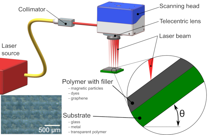
Figure 1: A sketch of the laser machining setup with the main elements. Circular zoom-in: the sample can be tilted to create tilted surface microstructures. Possible polymer and substrate options are described. Left bottom: An optical image of rectangular pillars is shown. Scale bar: 500 µm. Please click here to view a larger version of this figure.
2. Optical microscopy
NOTE: Make a preliminary characterization of structured MAE samples by using an optical microscope.
- Clean the sample using pressurized nitrogen gas and gently blow away potential dust or debris particles from the sample.
NOTE: Be careful not to use too strong bursts of gas, as that can potentially destroy the sample. - Place the sample on the microscope table and turn on the light source used in reflective microscopy. If the sample is deposited on a transparent substrate, use a transmissive light source.
- Choose the low magnification 10x objective and measure relevant lateral dimensions of the sample, for example, the pitch between lamellae (Figure 3A).
- Mount a camera on the top of the objective and pull the lever to redirect the light from the sample towards the camera sensor instead of the eyepiece.
- Configure the camera scale by capturing reference scale glass slide images. Measure the known distances in pixels to determine each objective's pixel size. Use open-source software like ImageJ to perform this scale calibration.
- Measure the chosen lateral dimensions of the sample in pixels, then calculate the physical distances by multiplying the number of pixels by the pixel size in micrometers.
- Switch to a higher magnification 40x objective to acquire structure height information.
- Open the field aperture to shallow the depth of the field.
- Adjust the micrometer stage height and focus the microscope on the top of the structures. Note down the number on the micrometer screw.
- Slowly raise the stage by turning the micrometer screw until the focus lies on the sample substrate. Note down the number on the micrometer screw.
- Estimate the height of the structure by subtracting the values on the micrometer screw before and after adjusting the focus (Figure 3A).
3. Scanning electron microscopy
NOTE: Acquire additional information about the surface of the MAE, like filler particle concentrations or surface roughness, with a scanning electron microscope (SEM).
- Connect to the SEM software and vent the pressure chamber.
NOTE: Position the potential samples in the SEM away from the detector column as it vents, to avoid detector contamination. - While the chamber is venting, prepare the samples for SEM following the steps below:
- Wear gloves. Cut the samples with a scalpel to the size of the SEM sample holder pin.
- Place a small piece of double-sided carbon tape on the pin, covering it whole. Trim the tape by extending it over the pin edges.
- Adhere the trimmed samples to the pins using plastic tweezers to avoid damaging the samples.
- Clean the samples using pressurized nitrogen gas and gently blow away potential dust or debris particles from the sample.
NOTE: Do not use too intense bursts of gas, as that can potentially destroy the soft elastomeric samples. - (optional) Coat the samples with a thin conductive layer of carbon or gold because it ensures less charge build-up and drift during longer measurements.
- Open the vacuum chamber and pull out the stage. Insert the pins with the samples in the stage while noting their positions. Return the stage to its primary position and close the vacuum chamber.
- Perform the backscattered electron measurements.
NOTE: Use the strong backscattering of electrons from larger atoms to generate contrast in material composition, as shown in Figure 3B, backscattered electrons. Measure particle shapes and sizes, concentration, and laser-ablation-induced particle changes by gathering backscattered data.- Pump the air from the vacuum chamber to achieve a high vacuum. Take an optical navigational photo of the samples and use it as a guide to move the stage to place the sample of interest at the correct distance from the detector edge.
NOTE: While driving the stage, constantly monitor its movement using the live infrared camera to avoid collisions. - Turn on the electron beam and display the image from the concentric backscatter detector (CBS). Adjust the beam strength and shape by choosing a 30 kV accelerating voltage, 4.0 spot size, and a 5 µs dwell time.
- Find the focus on the sample using either manual or auto adjustments. Set the correct brightness and contrast while viewing the histogram of the acquired image and maximize the histogram width.
- Choose the proper region of the sample and the desired magnification, and potentially readjust the focus.
- Pump the air from the vacuum chamber to achieve a high vacuum. Take an optical navigational photo of the samples and use it as a guide to move the stage to place the sample of interest at the correct distance from the detector edge.
- Perform the secondary electron measurements.
NOTE: Note that secondary electrons are generated along the electron path through the sample, however, only secondary electrons from the topmost surface layers escape the sample and are detected. By gathering secondary electron data with very low accelerating voltages, surface topography, where contrast stems from surface inclinations, is observed in Figure 3B of secondary electrons.- Turn off the electron beam. Move the sample holder away from the detector to a safe position. Set a low vacuum in the chamber of 0.70 mbar. Set the detector bias to 68%.
- Move the samples to a working distance of around 3.5 mm. Set a small accelerating voltage of 2.0 kV and a more prominent spot size 7. Increase the dwell time to 100 µs.
- Turn on the beam and display the detected image from the low-vacuum secondary electron detector (LVD). Find the focus and the correct brightness and contrast.
- Choose the proper region of the sample and the desired magnification, and potentially readjust the focus.
- After measurements, place the holder in the safe position and vent the vacuum chamber.
- While wearing gloves, open the chamber doors, remove the pins with the samples, and, using tweezers, peel the carbon tape from the pin.
- Save the samples for potential remeasurements. Close the chamber doors and leave the SEM in a high vacuum.
4. Magnetic manipulation
NOTE: Employ the setup shown in Figure 2, using an electromagnet with a 20 mm pole face to deform lamellar surfaces. Drive the electromagnet with a DC power supply, and observe the resulting deformations using a camera paired with a 10x objective.
- Place a nonmagnetic holder between the magnet poles. Above, construct a microscope by coupling the objective to a 200 mm tube lens that focuses the light on the camera detector. Design the objective-detector system to allow for translations in XYZ directions (Figure 2).
- Clean the sample using pressurized nitrogen gas and gently blow away potential dust or debris particles from the sample. Do not use too intense bursts of gas, as that can potentially destroy the soft elastomeric sample.
- Attach a piece of double-sided scotch tape to the sample holder and place the sample atop it in the center between the poles.
NOTE: For easier sample handling, use a polyvinyl alcohol (PVA) water-soluble glue to glue the samples onto microscope glass slides (glass also adheres better to tape than the elastomer). - Connect the power cables of the electromagnet to the power supply and connect to the camera using an appropriate connection cable.
- While capturing images, apply a 3.2 A direct current to the electromagnet, which produces a homogeneous magnetic field of around 340 mT in the center of the 20 mm pole gap. The magnetic field deforms the MAE structures.
- Study the deformations by testing different structures, sample-magnetic line orientations, magnetic field strengths, and dynamical field switching (Figure 4).
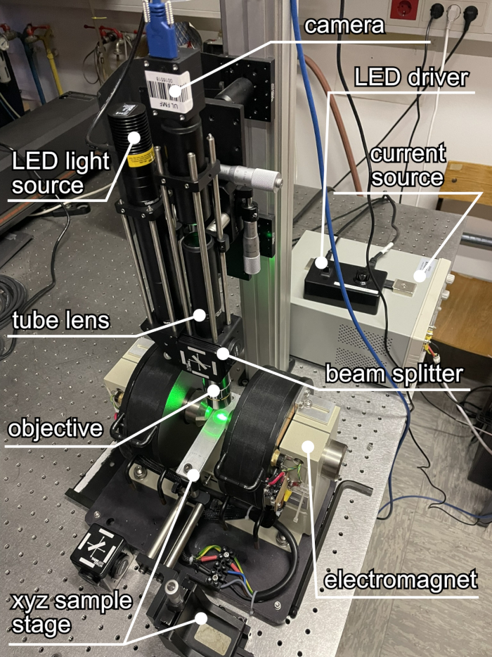
Figure 2: A photograph of the magnetic manipulation setup with the main components indicated. Please click here to view a larger version of this figure.
Results
Once the MAE surface is structured, it is inspected with optical microscopy. This is usually sufficient to confirm that the surface pattern is free from defects and to check that both lateral and vertical dimensions are as expected (Figure 3A). SEM is chosen if there is interest in further details, such as the particle distribution within the polymer matrix or the effect of the laser machining on the polymer surface roughness (Figure 3B).
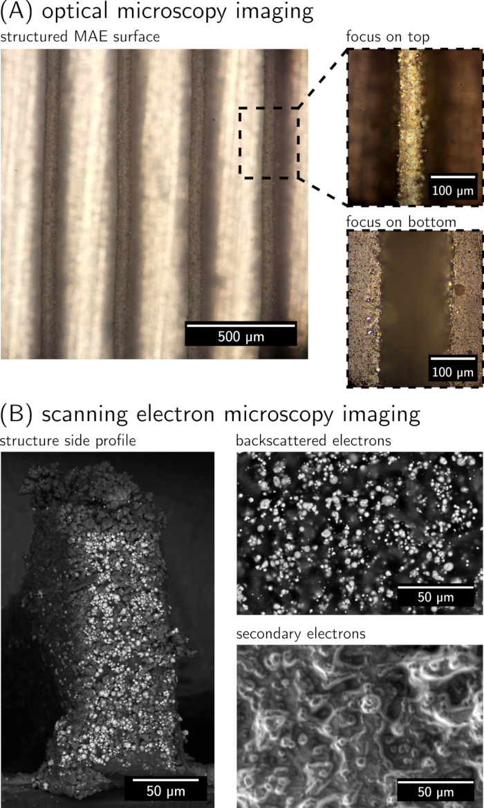
Figure 3: Optical images of a structured MAE surface. (A) Using a high-magnification objective, a preliminary structure characterization can be performed in lateral and longitudinal directions by varying the focus. The scalebar of the main image is 500 µm, and the scalebars in the magnified images are 100 µm. Additional surface characterizations are done with SEM (B), where different types of electrons can be detected and different surface properties measured. Backscattered electrons reveal compositional contrast, while secondary electrons offer insights into the topographical variation of the surface. All the scale bars are 50 µm. Please click here to view a larger version of this figure.
The protrusion orientation can be manipulated with time-varying magnetic fields, which can be created in various ways. Coils can produce electronically switchable fields or permanent magnets that are mechanically moved. Usually, magnetic fields are non-uniform, but if uniform magnetic fields are needed, the inside of solenoids or coils in the Helmholtz configuration can be utilized23.
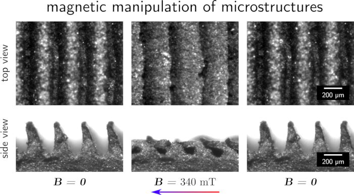
Figure 4: An example of the structure deformation control by a magnetic field. Using an electromagnet, a homogeneous magnetic field in the sample plane can be generated, inducing elastic deformations of surface structures. These deformations, in turn, induce changes in the macroscopic surface properties of MAE materials. The scale bars shown apply to all the images and are 200 µm. Please click here to view a larger version of this figure.
| Ingredient | Weight percent |
| Polymer VS 100000 | 7.07 |
| Modifier 715 | 0.03 |
| Polymer MV 2000 | 1.26 |
| Silicone oil | 16.62 |
| Carbonyl iron particles | 74.79 |
| Crosslinker 210 | 0.12 |
| Inhibitor DVS | 0.03 |
| Catalyst 510 | 0.08 |
| SUM | 100 |
Table 1: The ratio of chemicals in the MAE material formulation given by weight percent.
Discussion
Physical machining of the molds is optimal for large-scale production when the geometry of the surface features is already pre-set. In contrast, rapid prototyping is desirable at the development and optimization stage of a novel device. Both 3D printing of molds and direct laser photolithography have a fast turn-around time but have limitations. One disadvantage of 3D printed structures is that the molds' roughness leads to difficulties separating the casted polymer without rupture and damage. Direct laser photolithography is limited to orthogonal patterns to the surface. It is also suitable only for polymers that do not scatter the incoming light and are sufficiently transparent to enable photopolymerization throughout the polymer layer thickness. It is possible to use a photosensitive polymer to create a mold for another type of polymer, but this increases the fabrication time and prolongs prototype development. In contrast, laser machining is a moldless method that enables the direct structuring of optically absorbing polymers. This makes it perfectly suitable to create topographical features on polymers such as magnetoactive elastomers (MAEs), which gain absorption from a large concentration of magnetically responsive microparticles. Very distinctively, it also enables the production of non-orthogonal features, such as slanted or inclined walls3.
Laser micromachining
The laser micromachining technique described in step 1 is very robust, but particular attention should be put to the setup of the MAE sample. The distance from the lens should be carefully defined by accurately finding the focal plane on the sample's surface while also being parallel to the focusing lens plane because of the short Rayleigh distance provided by the laser system setup. A different approach is taken when fabricating slanted structures, compensating the sample's surface tilt by raising/lowering the sample to keep the current working area always in the focal plane. If the heat accumulation in the sample is too big (evaluated offline, after the micromachining, by visually checking the structures) and eroding the structures, suitable heat management should be employed.
Limitations of the approach are tied to the material filler particle size, which defines the lateral resolution of the process, and to the sample's optical properties, i.e., absorbance at the employed wavelength. Experimentally, we discovered that the minimum structure width that still withstands the laser micromachining is about five times the mean size of the filler particles3. If the target structures are smaller than that, the laser will remove all the material, resulting in a non-structured surface (albeit its roughness will be greater). For the material presented here, the specific laser light wavelength is predominantly absorbed by iron microparticles while it passes through the polymer. Changing the laser wavelength and the particle or polymer material can significantly alter the results. Test structuring is, therefore, a critical point for obtaining the processing parameters for new material.
The method described provides flexibility regarding structure size and the possibility of fabrication of tilted structures without the need for specialized molds. Also, the problem of MAE agglutination on mold removal is absent when employing this micromachining method. Compared to bottom-up spray coating under a magnetic field, this method provides higher spatial resolution and the possibility of fabricating ordered surface structure arrays. The micromachining method is used in research areas where micrometer-sized active structures are required to develop new devices for, i.e., surface wetting control, microfluidics, or transport of mm-sized solid particles or droplets.
Optical microscopy
Iron microparticles in MAE absorb a lot of light, while the base polymer, polydimethylsiloxane, is optically transparent. Observing the MAE surface roughness optically is challenging because imaging the polymer is required. For these kinds of measurements, an SEM is a better choice of equipment. On the other hand, the presence of iron microparticles in the MAE means that much light is required to observe the material. A common workaround is to capture images with a long exposure time and allow the detector to gather enough light.
Optical microscopy is a fast method for qualitative and quantitative analysis of samples. Changing the image focus is not the most accurate method, but it is comparable to the accuracy of the laser machining method. At 40x magnification, the axial resolution is very good (1 µm). Due to the roughness of the sample surface, the sample height is not well defined at those length scales, so an average height is measured instead with estimated uncertainties around 5 µm. The height versus the number of laser passes is found in Kravanja et al.3, where the smallest error bar is ±4 µm. If greater precision is needed, for example, examining the roughness of the protrusion surface, an excellent alternative is scanning confocal microscopy.
Observing magnetically induced changes in vivo under the microscope is not advisable, as the strong magnetic fields can magnetize microscope components and interfere with other magnetic-sensitive measurements. Consequently, a custom-built setup is used here for magnetic manipulation observation.
Scanning electron microscopy
SEM is a very versatile measurement technique for observing material surfaces. By choosing different detectors, it is possible to gather topographical and compositional data, revealing the surface ablation-induced roughness and composite structure of MAEs. It is important to note that MAEs are generally not electrically conductive, so specific measures must be taken to avoid electron build-up on the sample surface. It is possible to coat the samples with a carbon spray or gold sputtering that renders the surface conductive. It is also beneficial to employ a small spot size and short dwell times or a low vacuum where water vapor screens the charges on the sample surfaces. Large spot size and long dwell times in high vacuum can damage the samples.
This material has an iron particle concentration that is too large (close to the percolation threshold) for any currently available non-invasive method to penetrate deep into the sample without producing too many artifacts, scattering, and noise in the measurement. The only exception is neutron scattering experiments, though they require specialized facilities that are not easily accessible. However, SEM can still be employed to image the particle distribution throughout the sample using backscattered electron measurements for samples cut by a blade24. It has been revealed that the particle distribution is uniform, except for the depletion layer, which is believed to be connected to sedimentation during curing. SEM is limited by the absence of magnetic field-induced measurements, which are most interesting from the applicational standpoint.
Magnetic manipulation
Magnetic manipulation of MAE structures can be achieved either in the vicinity of a permanent magnet or between the pole shoes of an electromagnet. In the present work, the experiments were performed with an electromagnet due to easier control of the magnetic field values. A long-distance object lens for sample observation was employed to avoid undesired magnetization of the microscope parts. The lens had a working distance of 34 mm, which allowed it to be positioned sufficiently far away from the magnetic pole shoes, where the field strength vanished.
It is essential to acknowledge that samples made from a single MAE piece, partially structured on the surface, are also elongated in a homogeneous magnetic field. So, the deformations of microstructures were superimposed over sample stretching. To correctly measure structure deformations, the overall stretching contributions must be subtracted.
An electromagnet did not have an instantaneous magnetic field response to changing source voltage, but the time constant of the electrical circuit limited the transient response.11 The DC power supply's current output must be synchronized with the camera's image capture for dynamic experiments. It is possible to either measure the electrical current through the electromagnet and calculate the generated magnetic field or to directly measure it using a teslameter. However, in the latter case, the bandwidth of the teslameter should be considered as well.
Having set up a microscope in proximity to an electromagnet, the geometrical parameters of the structured MAE surface could be measured, as well as their dynamic changes. It was also possible to perform characterization relevant to the desired application, for example, the contact angles of droplets on such surfaces and how they dynamically change.
Disclosures
The authors have no conflicts of interest to disclose.
Acknowledgements
The authors are grateful for the funding by the Slovenian Research Agency (ARIS) research programs P1-0192, P2-0231, and P2-0392, research project J1-3006, Deutsche Forschungsgemeinschaft (DFG, German Research Foundation) - project numbers 437391117, 524921900, and within the framework of the GREENTECH project, co-financed by the European Union – NextGenerationEU. This research has also been partially supported by the Slovenian-German bilateral research project (ARIS: BI-DE/25-27-003 and the German Academic Exchange Service (DAAD) Projekt-ID: 57753025). We are grateful to Evonik Operations GmbH, Specialty Additives, Geesthacht, Germany, for providing chemicals for the synthesis of PDMS and to BASF SE, Ludwigshafen am Rhein, Germany, for providing carbonyl iron powder.
Materials
| Name | Company | Catalog Number | Comments |
|---|---|---|---|
| 10x Plan Apochromat Objective | Mitutoyo | MY10X-803 | used in Method 4 |
| 10x Objective | Nikon | cannot be determined | used in Method 2, air objective |
| 40x Objective | Nikon | cannot be determined | used in Method 2, air objective |
| Beam expander | SPI Lasers UK | PT-P00554 | |
| Camera | Canon | EOS M200 | used in Method 2 |
| Camera | FLIR | BFS-U3-17S7M-C | used in Method 4 |
| Carbonyl iron particles | BASF SE | CIP SQ | mean diameter D50 of 3.9-5.0 µm |
| Catalyst 510 | Evonik Operations GmbH, Specialty Additives | Catalyst 510 | |
| Crosslinker 210 | Evonik Operations GmbH, Specialty Additives | Crosslinker 210 | |
| DC power supply | GW Instek | GPD-3303S | |
| Electromagnet | GMW | 3470 | |
| Inhibitor DVS | Evonik Operations GmbH, Specialty Additives | Inhibitor DVS | |
| Laser source | SPI Lasers UK | SP-020P-A-HS-S-A-N | |
| Microscope | Nikon | OPTIPHOT2-POL | |
| Modifier 715 | Evonik Operations GmbH, Specialty Additives | Modifier 715 | |
| Polymer MV 2000 | Evonik Operations GmbH, Specialty Additives | Polymer MV 2000 | |
| Polymer VS 100000 | Evonik Operations GmbH, Specialty Additives | Polymer VS 100000 | |
| Scanning electron microscope | ThermoFisher | AXIA-CHEMISEM | |
| Scanning head | Raylase | SSIIE-10 | |
| Silicone oil | Wacker Chemie AG | AK 10 | |
| Stage micrometer 1mm | Nikon | MBM11100 | size reference glass slide |
| Stepper motor | Isert-electronic | P Series Nema 24 Bipolar 1.8deg 3.5Nm | 2 phase stepper motor, 1.8° step angle |
| Telecentric lens | Ronar-Smith | TSL-1064-18-56-V1 |
References
- Howland, F. L., Poole, K. M. Device Photolithography: An Overview of the New Mask-Making System. Bell System Technical Journal. 49 (9), 1997-2009 (1970).
- Gurkan, U. A., et al. Next generation microfluidics: fulfilling the promise of lab-on-a-chip technologies. Lab Chip. 24 (7), 1867-1874 (2024).
- Kravanja, G., et al. Laser micromachining of magnetoactive elastomers as enabling technology for magnetoresponsive surfaces. Adv Mater Technol. 7 (5), 2101045(2022).
- Zhang, M., Feng, S., Wang, L., Zheng, Y. Lotus effect in wetting and self-cleaning. Biotribology (Oxf). 5, 31-43 (2016).
- Zhang, Z., Chen, Z., Shang, L., Zhao, Y. Structural color materials from natural polymers. Adv Mater Technol. 6 (11), 2100296(2021).
- Nadzharyan, T. A., Shamonin, M., Kramarenko, E. Y. Theoretical modeling of magnetoactive elastomers on different scales: a state-of-the-art review. Polymers (Basel). 14 (19), 4096(2022).
- Shamonin, M., Kramarenko, E. Y. Highly responsive magnetoactive elastomers. Novel magnetic nanostructures. , Elsevier. 221-245 (2018).
- Kalina, K. A., et al. Multiscale modeling and simulation of magneto-active elastomers based on experimental data. Phys Sci Rev. 8 (1), 1-31 (2023).
- Kriegl, R., et al. Tunable rebound of millimeter-sized rigid balls by magnetic actuation of elastomer-based surface microstructures. Smart Mater Struct. 33 (6), 067001(2024).
- Jezeršek, M., et al. Control of droplet impact through magnetic actuation of surface microstructures. Adv Mater Interfaces. 10 (11), 2202471(2023).
- Straus, I., et al. Dynamically tunable lamellar surface structures from magnetoactive elastomers driven by a uniform magnetic field. Soft Matter. 19 (18), 3357-3365 (2023).
- Yang, Z., Park, J. K., Kim, S. Magnetically responsive elastomer-silicon hybrid surfaces for fluid and light manipulation. Small. 14 (2), 1702839(2018).
- Kriegl, R., et al. Microstructured magnetoactive elastomers for switchable wettability. Polymers (Basel). 14 (18), 3883(2022).
- Kravanja, G., et al. Magnetically actuated surface microstructures for efficient transport and tunable separation of droplets and solids. Adv Eng Mater. 25 (22), 2301000(2023).
- Wei, C., Zong, Y., Jiang, Y. Bioinspired wire-on-pillar magneto-responsive superhydrophobic arrays. ACS Appl Mater Interfaces. 15 (20), 24989-24998 (2023).
- Zhou, Y., Huang, S., Tian, X. Magnetoresponsive surfaces for manipulation of nonmagnetic liquids: design and applications. Adv Funct Mater. 30 (6), 1906507(2020).
- Li, C., et al. Directional transportation on microplate-arrayed surfaces driven via a magnetic field. ACS Appl Mater Interfaces. 13 (31), 37655-37664 (2021).
- Kim, J. H., et al. Remote manipulation of droplets on a flexible magnetically responsive film. Sci Rep. 5 (1), 17843(2015).
- Demirörs, A. F., et al. Amphibious transport of fluids and solids by soft magnetic carpets. Adv Sci (Weinh). 8 (21), 2102510(2021).
- Wang, L., et al. Dynamic magnetic responsive wall array with droplet shedding-off properties. Sci Rep. 5 (1), 11209(2015).
- ul Islam, T., et al. Microscopic artificial cilia-a review. Lab Chip. 22 (9), 1650-1679 (2022).
- Gu, H., et al. Magnetic cilia carpets with programmable metachronal waves. Nat Commun. 11 (1), 2637(2020).
- Helmholtz coil. , Wikipedia contributors. https://en.wikipedia.org/wiki/Helmholtz_coil (2025).
- Straus, I., et al. Surface modification of magnetoactive elastomers by laser micromachining. Materials (Basel). 17 (7), 1550(2024).
Reprints and Permissions
