We introduced a novel imaging technique called Optical Multilayer Interference Tomography (OMLIT), which enables unbiased imaging of all cells in brain specimens at the mesoscale and can be seamlessly integrated into the imaging workflow of tape-based serial scanning electron microscopy on the same sample.
A subscription to JoVE is required to view this content. Sign in or start your free trial.
Method Article
A Scanning Electron Microscopy-Compatible Optical Imaging Method for Mesoscopic All-Cell Brain Mapping
In This Article
Summary
Abstract
Understanding the structural and functional relationships within complex neural networks in the brain requires the construction of brain atlases that possess both a broad field of view and subcellular resolution. However, current optical and electron microscopy imaging methods each have limitations, making it difficult to image all cells within a single specimen. This protocol introduces an imaging technique called Optical Multilayer Interference Tomography (OMLIT), which enables indiscriminate optical imaging of all cells in brain specimens made following electron microscopy sample preparation, thereby reconstructing a complete brain atlas of all neural cells. In addition, OMLIT imaging can be seamlessly integrated with the imaging workflow of automated tape-collecting ultramicrotomy scanning electron microscopy (ATUM-SEM). This allows researchers to obtain mesoscale structural information of cells prior to electron microscopy imaging, facilitating the precise selection of regions of interest and significantly reducing the area and data volume required for high-resolution electron microscopy (EM) imaging. We validated the accuracy and compatibility of this method in actual samples from the adult mouse cerebral cortex, demonstrating its broad application prospects in multi-scale brain atlas construction.
Introduction
Comprehensive mapping of neural circuits at cellular and subcellular resolution is essential for revealing the structure and function of the brain. Traditional optical imaging methods, such as two-photon microscopy1, fluorescence micro-optical sectioning tomography (fMOST)2,3,4, and the VISoR system5, have enabled mesoscale neuronal imaging and in vivo functional imaging. However, due to their reliance on sparse labeling, they fail to capture the complete cellular population. On the other hand, label-free optical imaging techniques, such as functional photoacoustic microscopy (fPAM)6,7, optical coherence tomography (OCT)8, and quantitative phase microscopy9, hold the potential to visualize all neurons within the field of view simultaneously. Nevertheless, these methods are typically limited by low axial resolution and shallow imaging depth, and their hardware complexity hampers widespread application in brain atlas construction. In contrast, serial-section electron microscopy (ssEM) techniques, including serial block-face SEM (SBF-SEM)10,11, focused ion beam SEM (FIB-SEM)12,13,14, and automated tape-collecting ultramicrotomy SEM (ATUM-SEM)15,16,17, can reveal dense synaptic connectivity networks at nanometer resolution, providing essential tools for high-resolution connectomics. However, these techniques suffer from low throughput, long acquisition times, limited fields of view, and high data processing and hardware costs18.
To overcome the above limitations, we developed an imaging method named Optical Multilayer Interference Tomography (OMLIT), which offers a low-cost and high-throughput solution for indiscriminate, high-contrast, wide-field imaging of all cells on ultrathin sections, achieving submicron resolution across large tissue areas. At the same time, OMLIT is inherently compatible with serial-section SEM workflows: before high-resolution electron microscopy, OMLIT provides structural information on the same sections, allowing precise ROI navigation and significantly reducing the area and data volume required for subsequent EM imaging. OMLIT offers unique advantages at the mesoscale imaging level and serves as a critical bridge connecting neural structural maps across different spatial scales. Its non-destructive nature preserves the potential for future integration with specific labeling strategies, such as the use of osmium-resistant fluorescent proteins19 for sample preparation and imaging. This method enables mesoscale imaging of selected brain regions, allowing rapid acquisition of neuronal morphology, quantity, distribution, and density in the regions. It also facilitates quantitative characterization of axonal projections and dendrite distribution between neurons in different brain areas. For specific regions of interest in the imaging results, in situ ultrastructural details can be further investigated using electron microscopy.
The imaging principle of OMLIT has been described in the work by Hao Fan20. Briefly, during imaging, the ultrathin section, coated layer, collection tape, conductive tape, and wafer form a multilayer thin-film structure. When a plane wave interacts with this structure, reflected waves are generated at various interfaces and overlap in the detection space, resulting in optical interference due to differences in reflectance, refractive index, and absorption among the materials. A MATLAB-based simulation program developed based on this principle demonstrated reasonable agreement with experimental results.
The OMLIT imaging scheme can be categorized into two types based on the tape processing strategy. The first is the high-reflectivity strategy, in which metals such as Cr, Cu, Al, or Ag are used to coat the tape surface, resulting in higher optical intensities in cytoplasmic regions and resin-filled vascular lumens compared to surrounding areas. The second is the low-reflectivity strategy, which employs uncoated Kapton tape, D-50 tape, or CNT-coated PET tape. In this case, the optical imaging outcome is the reverse of the first: resin-rich membrane-free regions (e.g., cytoplasm and vascular lumens) appear with lower intensity.
We systematically summarize and establish standardized protocols tailored to two distinct imaging strategies. The protocols presented here offer comprehensive and detailed experimental procedures. Additionally, common issues encountered during the experiments are summarized, along with proposed solutions. We focus on presenting a dataset of mouse cortex acquired using the low-reflectivity strategy (805 × 857.5 × 11.66 µm³), illustrating the distinctive features and advantages of the OMLIT imaging approach.
Access restricted. Please log in or start a trial to view this content.
Protocol
All animal procedures were performed in accordance with the institutional guidelines of the University of Science and Technology of China and relevant national regulations. The sample preparation for OMLIT imaging follows the same protocol as that used in conventional EM, and the specific procedure we employed has been described elsewhere21.In brief, after anesthesia, mice were transcardially perfused sequentially with sodium cacodylate buffer, artificial cerebrospinal fluid (ACSF), and finally a fixative containing glutaraldehyde and paraformaldehyde. The brain was carefully removed, and around 1 × 1 × 1 mm³ blocks of brain tissue were sectioned. The samples were then chemically fixed, subjected to serial heavy metal staining, dehydrated, and embedded in resin. The general workflow of the protocol is presented in Figure 1.
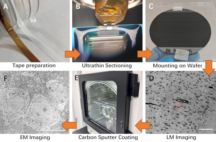
Figure 1: Overview of the workflow. (A) Collection tapes mentioned in the protocol (from left to right: polyimide, D-50, and CNT-coated PET). (B) Serial sectioning and collection of the trimmed samples. (C) Mounting of ribbons containing collected sections onto a circular silicon wafer. (D) Light microscopy imaging, scale bar 100 µm. (E) Carbon coating. (F) Electron microscopy imaging corresponds to the region outlined in Figure 1D, scale bar: 10 µm. Please click here to view a larger version of this figure.
1. Tape preparation
NOTE: The following procedures should be performed in a cleanroom to prevent tape contamination from dust.
- High-reflectivity strategy
- Select Kapton (henceforth referred to as polyimide tape, 50 µm thickness) or Panlite film (henceforth referred to as D-50, 50 µm thickness) and mount it onto the motorized winding system. Here, the polyimide tape is used as an example.
NOTE: A motorized winding device, designed to be driven by a stepper motor controlled through an Arduino board, to run the tape from one reel to the other through the sputter plasma cone, was used in this study. To compensate for the increasing line speed of tape translation caused by the accumulation of tape on the driving reel, increasing the take-up reel diameter, a program was written to serially tune down the take-up reel's angular speed after each 360° rotation. - Deposit a uniform thin film of Cr (or other metals such as Al, Ag, or Cu) onto the surface of the tape using a magnetron sputtering system (double-head sputter). Position the tape at a distance of 80 mm from the sputtering target for optimal deposition. Conduct the process under DC power and at a pressure of 1.0 Pa regulated by 99.99% argon gas.
- Set the tape winding speed to 0.6 mm/s to achieve a metal coating thickness of 50 nm. After deposition, cool the chamber slowly to room temperature (RT) under high vacuum to minimize coating stress.
NOTE: The optimal coating thickness for the same tape can vary depending on the type of metal used. Adjust the translation speed of the tape to achieve a variety of coating thicknesses, such as 50, 70, 100, 150, and 200 nm. - Evaluate the thickness and uniformity of the coating using a stylus profiler, atomic force microscopy, or scanning electron microscopy.
- Clean and render the tape hydrophilic using a plasma cleaner at 80 W power, with a tape moving speed of 7 mm/s. After treatment, water droplets placed on the tape surface should rapidly spread into a thin film (Figure 2A).
- Select Kapton (henceforth referred to as polyimide tape, 50 µm thickness) or Panlite film (henceforth referred to as D-50, 50 µm thickness) and mount it onto the motorized winding system. Here, the polyimide tape is used as an example.
- Low-reflectivity strategy
NOTE: This protocol allows the use of either D-50 tape or a commercial carbon nanotube (CNT)-coated polyethylene terephthalate (PET) tape. Since the latter may introduce some background noise during electron microscopy imaging-although not strong-it could potentially affect the segmentation of EM images. Therefore, the following description will still use the D-50 tape as an example.- Prepare the D-50 films and cut the full sheet into tapes approximately 7 mm wide. Use one exposed side of the tape for collecting sections, while protecting the other side with a layer of matte film to prevent scratches and contamination. Remove the matte film during the subsequent silicon wafer mounting step.
- For larger numbers of sections, join different sections of D-50 tape together. Secure the joints between tape segments using double-sided adhesive tape.
NOTE: When adhering tape segments, ensure that the leading tape overlaps the trailing one from top to bottom via the double-sided tape. Minimize the adhesive area and leave a margin along the tape edges to prevent glue from being squeezed out during tape winding, which may contaminate the tape (Figure 2B). - Clean and render the tape hydrophilic using a plasma cleaner, following the same procedure and achieving the same effect as previously described.
NOTE: Except for the metal coating and carbon sputtering steps, the other steps in both strategies are the same.
2. Serial ultrathin sectioning and tape-based collection
- Using a small grinder or similar cutting tool, rough-trim the resin on the side with the sample, removing the surrounding blank resin to expose the sample area.
- Place the resin-embedded block in the sample holder, and tighten the knob of the holder to secure the block firmly.
- Mount the sample holder on the microtome's movable arm. Install a glass knife or diamond trimming knife (at a 45° angle) on the knife holder. Under the microscope, trim the sample surface into a pyramid shape and smooth the surface.
NOTE: The front and back edges of the trimmed sample block should be as parallel as possible (see Figure 2C). - Trim and smooth the four sides of the sample block to remove any excess resin around the edges, preventing potential collisions with the diamond knife. Rotate the knob to ensure that the front and rear edges of the trimmed block are aligned in a horizontal position.
- Remove the trimming knife and replace it with a diamond knife set at a 45° angle. Set the tilt angle of the microtome base to 6°. Slowly move the knife holder using the knob until the front edge of the diamond knife is 1-2 mm from the sample surface.
- Observe the bright band between the sample surface and the knife edge, and adjust the tilt angle so the band is even top-to-bottom and side-to-side. This helps ensure the first section includes the entire sample surface, not just a corner.
- Inject distilled water into the groove of the diamond knife, allowing the liquid level to rise and ensuring the blade is wet. Then, use a syringe to remove some of the water until the liquid level dips, and the reflection appears silvery.
- Set the section thickness (feed), cutting speed, and cutting window in the control unit. Adjust the sectioning speed to 0.6 mm/s and set the section thickness to 60 nm (the specific speed and thickness depend on the sample quality).
- Begin sectioning. Once the microtome runs stably and uniform sections are produced, pause the sectioning process. Use a fine brush to remove the cut sections and any debris.
- Install both the coated tape reel and an empty take-up reel on the automatic ultrathin section collecting system. Secure the locking mechanism and perform a trial run to ensure the tape moves smoothly at a constant speed and is properly collected onto the empty reel.
- Immerse the collection head of the tape collection device in the water bath of the diamond knife. Adjust the position of the collection head so that it is parallel to the knife edge, at a distance of 1.5 times the sample slice length, ensuring that the cut sections are smoothly collected onto the tape. Secure the collection device and resume sectioning while simultaneously running the tape collection device.
- After collecting a sufficient number of continuous sections, pause the sectioning process. Cut the tape in the section area where no sections were collected, and continue running the tape collection device until all the remaining tape is collected onto the spool.
- Remove the spool containing the collected sections and place it in an electronic drying oven. Clean the tape collection device and the microtome, and return all accessories to their proper places.
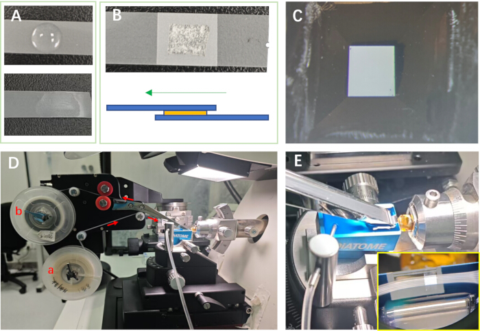
Figure 2: Preparations before sectioning. (A) Water droplets on the surface of the D-50 tape before (top) and after (bottom) hydrophilic treatment. (B) Top and side schematic views of the junction area of the D-50 tape. Blue: D-50 tape; orange: double-sided adhesive; green arrow: tape movement direction. (C) Frontal view of the sample after trimming, showing parallel top and bottom edges. (D) Automated tape collection device. a: Tape spool for D-50 tape feeding-out; b: Tape spool for tape retrieval; red arrow: direction of tape movement. (E) Position of the collection head on the automated tape collection device. The yellow box at the lower right indicates a freshly cut section about to be collected by the device. Please click here to view a larger version of this figure.
3. Mounting on a silicon wafer
NOTE: Ensure the workspace is clean to avoid contamination of the tape by dust during the following steps.
- Use a 4-inch round silicon wafer pre-cleaned and hydrophilized in a plasma treatment system (at 80 W power, 3 min).
- Put on clean gloves, place the silicon wafer on a flat surface, and cut a piece of double-sided conductive carbon tape to an appropriate length (with 2-3 cm overhang on both ends). Peel off the white protective layer from one side of the double-sided conductive tape, and apply it from top to bottom onto the silicon wafer.
NOTE: The two sides of the conductive tape should be spaced about 2 mm apart, and the edges of the tape should be visible on the silicon wafer. For a 25 mm wide double-sided conductive tape, three segments of tape can be applied to one 4-inch silicon wafer. - Draw an outline of the 4-inch silicon wafer on the workbench and mark the approximate length of each segment of tape that will be applied to the wafer. Cut the tape that has collected the sections according to the lengths previously marked.
NOTE: The cut tape should not exceed the edge of the silicon wafer, and do not cut into the sections. - Peel off the transparent protective film from the double-sided conductive tape, and for D-50 tape, remove the protective film on the back of the tape at this point. Apply the tape parallel to the double-sided conductive tape. Apply up to three segments of tape to each piece of double-sided conductive tape.
NOTE: To reduce the risk of the D-50 tape being misaligned or contaminated by dust, cover part of the conductive tape with the transparent film that was previously peeled off, leaving only a small portion of the conductive tape exposed to attach the end of the D-50 tape. This allows for easier adjustment of the tape's direction. Afterward, slowly peel off the remaining transparent film, allowing the rest of the D-50 tape to fall gently and adhere to the conductive tape. - After the tape is mounted, air bubbles may form between the tape and the conductive tape, which can interfere with the subsequent imaging process. Place the silicon wafer in a vacuum chamber (or other vacuum equipment) and apply a vacuum. After the vacuum process is complete, ensure the air bubbles have disappeared.
4. Post-staining
- Prepare 4% uranyl acetate and 3% lead citrate, and preheat them to 50°C using a water bath pot.
CAUTION: Uranyl acetate is radioactive and has significant toxicity to the liver and kidneys. Lead citrate can cause lead poisoning, affecting the nervous system, kidneys, and hematopoietic system. Work with these reagents should be performed in a fume hood, and appropriate personal protective equipment (PPE), including a laboratory coat, nitrile gloves, mask, and safety goggles, should be worn. In case of skin or eye contact, immediately wash with copious amounts of water, report to lab safety personnel, and seek medical attention. - Place the silicon wafer, which has been vacuumed and is free of bubbles, into a plasma hydrophilization system for hydrophilization and cleaning.
- Using a 10 mL syringe with the needle removed, attach a 0.22 µm syringe filter and filter the 4% uranyl acetate. Drop the solution onto the section until the entire surface of the section on the silicon wafer is covered, and then wait for 3 min.
- Wash with distilled water for 3 min, repeating 3 times, and then blow-dry the sample surface with nitrogen.
- Using a 10 mL syringe with the needle removed, attach a 0.22 µm syringe filter and filter the 3% lead citrate. Drop the solution onto the section until the entire surface of the section on the silicon wafer is covered, and then wait for 5 min.
- Wash with distilled water for 3 min, repeating 3 times, and then blow-dry the sample surface with nitrogen.
5. Data acquisition
- Optical microscopy
NOTE: In this section, a Research Slide Scanner (VS200, Olympus) is used as an example for optical microscopy. Other microscopes, such as the Axio Imager.A2 Vario (Zeiss, Germany), are also suitable for the optical imaging described here. The steps for other optical microscopes are generally the same.- Place the silicon wafer on the stage of the optical microscope and secure it with non-residue adhesive tape.
- Use a 5x objective lens to obtain an overview image of the silicon wafer, the tape, and the sample.
- On the overview image, outline each section and sort them, then add focus points and exposure points to perform automatic imaging at 20x or 50x magnification across the entire silicon wafer with all sections.
- After imaging is completed, save the images, and then check the image quality. If there are any out-of-focus or poor-quality images, refocus and reimage.
- Electron microscopy
NOTE: Multiple types of electron microscopes can perform continuous imaging of ultrathin sections placed on silicon wafers. Here, the Multibeam 505 (Zeiss) is used as an example.- Perform carbon coating on the sample surface using a high-vacuum sputter coater, with a carbon thickness of 5.7 nm.
NOTE: This step can be skipped for tapes that have been metal-coated in a high-reflectivity strategy or coated with carbon nanotubes (CNT) in a low-reflectivity strategy. - Use an optical microscope (Axio Imager.A2 Vario, Zeiss) to capture the optical navigation map of the silicon wafer.
- Place the silicon wafer into the sample chamber of the SEM. Associate the optical navigation map with the electron microscope image by sequentially identifying the two nested L-shaped markers on the sample stage.
- Use the SAT module in the microscopy software (v3.2, 64-bit) to semi-automatically identify the section positions and imaging areas from the optical navigation map.
- Set the image pixel size to 4 nm, dwell time to 0.8 µs, focus points and positions, and storage locations.
- Begin continuous imaging.
- Perform carbon coating on the sample surface using a high-vacuum sputter coater, with a carbon thickness of 5.7 nm.
6. Data processing
NOTE: The 2D stitching of OMLIT images is automatically performed by the software. For large-scale 3D registration and segmentation of OMLIT images, other more powerful AI algorithms are available. Here, for the convenience of most laboratories to verify the process, the stitching, registration, and segmentation using Fiji (v1.54p, 64-bit) and VAST (v1.5.0, 64-bit) are demonstrated.
- Open the image dataset in Fiji by dragging the folder containing all the image files into the Fiji interface, and select Virtual Stack when prompted.
- Use the Rectangle Tool to select the region of interest (ROI), then crop the dataset via Image > Crop.
- Align the image stack using the Register Virtual Stack Slices plugin (Plugins > Registration > Register Virtual Stack Slices).
- Save the aligned dataset in TIFF format (File > Save As > Tiff).
- Import the TIFF image stack into VAST22 using Import > Import image volume from images to .VSV File.
NOTE: For a more detailed tutorial, please refer to the website: https://lichtman.rc.fas.harvard.edu/vast/ - By connecting an external tablet, use the brush tool in Draw Segment Mode to begin manual segmentation and tracing (use shortcut keys A and Z to quickly navigate between image slices).
- Visualize the segmented structure in 3D using Window > 3D Viewer > View > Update.
- Save the segmentation results via File > Save Segmentation.
Access restricted. Please log in or start a trial to view this content.
Results
The overall workflow of the protocol (Figure 1) begins with the preparation of different collection tapes. Figure 1 shows the three types of tapes mentioned in the protocol (from left to right: Kapton, D-50, and CNT-coated PET), which exhibit distinct optical properties when placed on the same background substrate. After sample preparation and block trimming, a few sections should be first collected for electron microscopy imaging to ensure the preparation meets...
Access restricted. Please log in or start a trial to view this content.
Discussion
Here, we developed an optical imaging approach, termed OMLIT, that enables mesoscopic imaging and is compatible with tape-based serial scanning electron microscopy workflows. By using the OMLIT method, optical microscopy can be employed to capture mesoscopic structural features from brain samples, including blood vessels, cell bodies, nuclei, major dendritic branches, and some large myelinated axons. In addition, OMLIT can be seamlessly integrated into the serial SEM pipeline, providing structural information prior to el...
Access restricted. Please log in or start a trial to view this content.
Disclosures
No conflicts of interest declared.
Acknowledgements
This work was supported by the National Science Foundation of China (32271430, 62361166631) and the Ministry of Science and Technology of China (2023YFF0715904). We thank the Public Technical Center of Suzhou Institute of Biomedical Engineering and Technology, and the Brain Imaging Facility of the Institute of Artificial Intelligence, Hefei Comprehensive National Science Center, for their support in OMLIT and serial EM imaging.
Access restricted. Please log in or start a trial to view this content.
Materials
| Name | Company | Catalog Number | Comments |
|---|---|---|---|
| Adhesive tape | 3M | B5005094008 | Double-sided adhesive |
| Atomic Force Microscope | Bruker | Dimension Icon | |
| Automatic ultrathin section collecting system | Lehua | AutoCUTS II | |
| Conductive adhesive tape | Ted Pella | FP16084-8 | |
| Dektak Stylus Profilers | Bruker | DektakXT | |
| Diamond knife for sectioning | Diatome | DUJ3530 | Diatome Jumbo knife |
| Diamond knife for trimming | Diatome | DTB90 | Glass knife |
| Electron microscope | Zeiss | MultiSEM505 | Alternative: GeminiSEM 300, Zeiss |
| FIJI (v1.54p, 64-bit) | Open source | https://fiji.sc | |
| Glass trimming knife | Selfmade | ||
| Lead Citrate | Leica | T534/2 | |
| Light microscope | Olympus | VS200 | Alternative: Axio Imager. A2 Vario, Zeiss |
| Light microscope | Zeiss | Axio Imager.A2 Vario | |
| Plasma cleaner | Yidon Technologies | Hydro-S4 | Alternatives: Ted Pella Pelco or other benchtop plasma cleaner |
| Polymer tape | Melton | Kapton | The website of the company is no longer accessible. We recommend that researchers try locally available KAPTON tapes. |
| Polymer tape | Teijin | PET | https://www.teijin.com/ |
| Polymer tape | Teijin | D-50 | https://www.teijin.com/ |
| Silicon wafer | Saichi | 912303 | Wafer is polished on one side. |
| Sputter Coater | Leica | ACE600 | Alternative:Double-head Sputter, Yujie |
| Ultramicrotome | Leica | UC7 | Alternative: RMC PT-PC |
| Uranylacetate | EMS | 22400 | |
| VAST (v1.5.0, 64-bit) | Howard Hughes Medical Institute | https://software.dvid.io/vast/ | VAST A1:D32Lite is a free tool for manual annotation and segmentation of large 3D microscopy datasets. |
| ZEN software (v3.2, 64-bit) | Zeiss | https://www.zeiss.com/microscopy/zh/products/software/zeiss-zen.html |
References
- Economo, M. N., et al. A platform for brain-wide imaging and reconstruction of individual neurons. eLife. 5, e10566(2016).
- Gong, H., et al. Continuously tracing brain-wide long-distance axonal projections in mice at a one-micron voxel resolution. Neuroimage. 74, 87-98 (2013).
- Zheng, T., et al. Visualization of brain circuits using two-photon fluorescence micro-optical sectioning tomography. Opt Express. 21 (8), 9839(2013).
- Lin, R., et al. Cell-type-specific and projection-specific brain-wide reconstruction of single neurons. Nat Methods. 15 (12), 1033-1036 (2018).
- Wang, H., et al. Scalable volumetric imaging for ultrahigh-speed brain mapping at synaptic resolution. Natl Sci Rev. 6 (5), 982-992 (2019).
- Yao, J., et al. High-speed label-free functional photoacoustic microscopy of mouse brain in action. Nat Methods. 12 (5), 407-410 (2015).
- Li, X., Kang, L., Zhang, Y., Wong, T. T. W. High-speed label-free ultraviolet photoacoustic microscopy for histology-like imaging of unprocessed biological tissues. Opt Lett. 45 (19), 5401(2020).
- Kut, C., et al. Detection of human brain cancer infiltration ex vivo and in vivo using quantitative optical coherence tomography. Sci Transl Med. 7 (292), (2015).
- Hu, C., Popescu, G. Quantitative phase imaging (QPI) in neuroscience. IEEE J Sel Top Quantum Electron. 25 (1), 1-9 (2019).
- Denk, W., Horstmann, H. Serial block-face scanning electron microscopy to reconstruct three-dimensional tissue nanostructure. PLoS Biol. 2 (11), e329(2004).
- Titze, B., Genoud, C. Volume scanning electron microscopy for imaging biological ultrastructure. Biol Cell. 108 (11), 307-323 (2016).
- Heymann, E. W. Scent marking strategies of new world primates. Am J Primatol. 68 (6), 650-661 (2006).
- Echlin, M. P., et al. Recent developments in femtosecond laser-enabled TriBeam systems. JOM. 73 (12), 4258-4269 (2021).
- Randolph, S., Geurts, R., Wang, J., Winiarski, B., Rue, C. Femtosecond laser-enabled TriBeam as a platform for analysis of thermally- and charge-sensitive materials. Microsc Microanal. 25 (S2), 352-353 (2019).
- Horstmann, H., Körber, C., Sätzler, K., Aydin, D., Kuner, T. Serial section scanning electron microscopy (S3EM) on silicon wafers for ultra-structural volume imaging of cells and tissues. PLoS One. 7 (4), e35172(2012).
- Hayworth, K. J., et al. Imaging ATUM ultrathin section libraries with WaferMapper: A multi-scale approach to EM reconstruction of neural circuits. Front Neural Circuits. 8, 68(2014).
- Schalek, R., et al. Development of high-throughput, high-resolution 3D reconstruction of large-volume biological tissue using automated tape collection ultramicrotomy and scanning electron microscopy. Microsc Microanal. 17 (S2), 966-967 (2011).
- Kasthuri, N., et al. Saturated reconstruction of a volume of neocortex. Cell. 162 (3), 648-661 (2015).
- Fu, Z., et al. mEosEM withstands osmium staining and Epon embedding for super-resolution CLEM. Nat Methods. 17 (1), 55-58 (2020).
- Fan, H., et al. Optical multilayer interference tomography compatible with tape-based serial SEM for mesoscale neuroanatomy. ACS Photonics. 9 (1), 25-33 (2022).
- Hua, Y., Laserstein, P., Helmstaedter, M. Large-volume en-bloc staining for electron microscopy-based connectomics. Nat Commun. 6 (1), 7923(2015).
- Berger, D. R., Seung, H. S., Lichtman, J. W. VAST (volume annotation and segmentation tool): Efficient manual and semi-automatic labeling of large 3D image stacks. Front Neural Circuits. 12, 88(2018).
- Shannon, C. E. A mathematical theory of communication. Bell Syst Tech J. 27 (3), 379-423 (1948).
- Tsai, D. -Y., Lee, Y., Matsuyama, E. Information entropy measure for evaluation of image quality. J Digit Imaging. 21 (3), 338-347 (2008).
- Wang, T., et al. A convenient all-cell optical imaging method compatible with serial SEM for brain mapping. Brain Sci. 13 (5), 711(2023).
- Kuwajima, M., Mendenhall, J. M., Harris, K. M. Large-volume reconstruction of brain tissue from high-resolution serial section images acquired by SEM-based scanning transmission electron microscopy. Methods Mol Biol. 950, 253-273 (2013).
- Kislinger, G., et al. ATUM-Tomo: A multi-scale approach to cellular ultrastructure by combined volume scanning electron microscopy and electron tomography. eLife. 13, e90565(2024).
- Böhm, T., Felfer, P., Thiele, S. A modular and automated serial section collection system for ultramicrotomy and subsequent imaging. Microsc Microanal. 29 (1), 212-218 (2023).
- Wacker, I. U., et al. Multimodal hierarchical imaging of serial sections for finding specific cellular targets within large volumes. J Vis Exp. (133), e57059(2018).
Access restricted. Please log in or start a trial to view this content.
Reprints and Permissions
