Описана установка рентгеновских лучей, индуцированных текущих измерений на синхротронных лучах. Он раскрывает наноразмерную производительность солнечных элементов и расширяет набор методов для мультимодальной рентгеновской микроскопии. От электропроводки до оптимизации сигнала и шума показано, как выполнять современные измерения XBIC на жестком рентгеновском микрозонде.
Методическая статья
Рентгеновский луч индуцированных текущих измерений для мульти-модальной рентгеновской микроскопии солнечных клеток
В этой статье
Уведомление об исправлении
Important: There has been an erratum issued for this article. View Erratum Notice
Краткое содержание
Аннотация
Рентгеновский луч индуцированных тока (XBIC) измерения позволяют отображение наноразмерных производительности электронных устройств, таких как солнечные батареи. В идеале XBIC используется одновременно с другими методами в рамках мультимодального подхода к рентгеновской микроскопии. Приведен пример, приведенный в настоящем месте, сочетающий XBIC с рентгеновской флуоресценцией, чтобы обеспечить точечную корреляцию электрической производительности с химическим составом. Для самого высокого соотношения сигнала к шуму в измерениях XBIC усиление блокировки играет решающую роль. При таком подходе рентгеновский луч модулируется оптическим вертолетом вверх по течению образца. Модулированный рентгеновский луч индуцированного электрического сигнала усиливается и модифицируется на частоту вертолета с помощью усилителя блокировки. Оптимизируя низкопроходимые настройки фильтра, частоту модуляции и амплимации, шум можно эффективно подавлять для извлечения четкого сигнала XBIC. Аналогичная установка может быть использована для измерения рентгеновского луча индуцированного напряжения (XBIV). Помимо стандартных измерений XBIC/XBIV, XBIC может быть измерен с прикладным светом или наклонным напряжением таким образом, чтобы условия работы солнечных батарей на открытом воздухе могли быть воспроизведены во время измерений на месте и операндо. В конечном счете, мультимодальная и многомерная оценка электронных устройств на наноуровне позволяет по-новому взглянуть на сложные зависимости между составом, структурой и производительностью, что является важным шагом на пути к решению материалов». Парадигмы.
Введение
В мире, где спрос на электрическую энергию постоянно растет, чистый и устойчивый источник энергии становится все более необходимым. Одной из возможностей для решения этих требованийявляются фотоэлектрические (PV) системы 1,2,3. Для направленного и эффективного способа разработки солнечных элементов следующего поколения необходимо понять,как состав и структура солнечных элементов влияют на их работоспособность 4. Типичные вопросы в развитии солнечных батарей включают: Какие типы дефектов являются наиболее пагубными, и где они расположены5,6? Есть ли неоднородности в элементарном распределении, и каково их влияние7,8,9? Как изменяются солнечные элементы при сборке модуля и старении10,11?
Как солнечный элемент только так хорошо, как его слабая часть, это особенно важно, чтобы понять влияние композиционных и структурных изменений на производительность в поликристаллических солнечных элементов, которые страдают по своей сути от неоднородности7, 8. Это особенно верно для тонкопленочных (TF) солнечных элементов, которые содержат слои амортизатора с кристаллитными размерами в диапазоне микрометров. Здесь влияние границ зерна на производительность представляет наибольший интерес, но их небольшой размер и тот факт, что они похоронены во всем слое стека создают уникальные проблемы характеристики. Кроме того, сложная химия многокомпонентных абсорбаторных слоев с сосуществующими фазами и внутренними градиентами требует сложных методов характеристик12.
Синхротрон на основе жестких рентгеновских микроскопов способны решать проблемы характеристики TF солнечных элементов: они обеспечивают рентгеновские размеры пятна до нанометровой шкалы13,14,15,16 и Глубина проникновения жестких рентгеновских лучей позволяет зондировать различные слои устройства17,в том числе зарытые слои поглотителя. С богатством различных методов измерения при сканировании рентгеновского микроскопа, становится возможным одновременно изучать не только один, но и множество различных аспектов солнечных элементов в рамках мультимодальных измерений и соотнести наблюдаемые характеристики. Например, рентгеновский луч индуцированных тока (XBIC) измерения успешно сочетаются с рентгеновской флуоресценции (XRF)7,18,19, рентгеновский возбужденный оптический люминесценции (XEOL)20, 21, и рентгеновская дифракция (XRD)22 для корреляции электрической производительности с составом, оптической производительности и структуры, соответственно23.
Во время XBIC измерений солнечных элементов или других устройств в стадии тестирования (DUT)24,25, инцидент рентгеновских фотонов отправился частицы душ, состоящий из электронов и фотонов, в результате чего множество возбужденных электрон-отверстие пар на рентгеновский фотон инцидента в полупроводниковом амортизаторе. Наконец, пары электрон-дыры термически к краям полосы поглотителя солнечных элементов. Таким образом, эти рентгеновские возбужденных носителей заряда можно рассматривать как заряд носителей, которые генерируются поглощения фотонов с энергиями чуть выше bandgap во время нормальной работы солнечных батарей, и в результате тока или напряжения могут быть измерены как рентгеновский снимок пучок индуцированный ток23,26,27 или напряжения (XBIV)28,29 похожи на более распространенные измерения, как электронный луч индуцированного тока (EBIC) или лазерного луча индуцированного тока (LBIC). Следовательно, сигнал XBIC/XBIV зависит не только от толщины слоя амортизатора, но и от электрической производительности DUT, как на микроскопическом, так и на макроскопическом уровне, включая локальный диапазон, расщепление уровня Ферми и рекомбинацию. Таким образом, мы можем составить карту локальных вариаций эффективности сбора заряда,носителя, которая определяется как вероятность того, что внешне возбужденная пара электрон-дыры в слое амортизатора собирается при электрических контактах DUT.
Обратите внимание, что только электронные отверстия пары, которые генерируются в амортизатор слой DUT способствовать XBIC / XBIV сигнала. Зарядные носители, генерируемые в других слоях, таких как металлические контакты или субстрат, немедленно рекомбинируются, так как они не имеют возможности быть разделенными соединением. Таким образом, другие слои влияют только на измерения XBIC/XBIV с помощью вторичных эффектов, таких как паразитическое поглощение рентгеновских лучей или выброс вторичных фотонов и электронов, которые могут быть повторно поглощены в слое абсорбатора. В отличие от этого, все слои потенциально способствуют сигналу XRF.
Учитывая, что сигналы XBIC и XBIV могут быть небольшими (часто, вариации в суб-picoampere и нановольт диапазоне представляют интерес), сигналы легко похоронили в шуме. Поэтому мы предложили использовать усилитель блокировки для извлечения сигналов XBIC и XBIV30. Для этой цели входящий рентгеновский луч модулируется оптическим измельчительом, как указано на рисунке 1. Эта модуляция переносится на сигнал, производимый DUT. Перед покажем сигналом в усилитель блокировки (LIA) предварительно усилитель (PA) обычно используется для сопоставления интенсивности необработанного сигнала с диапазоном аналогового цифрового конвертера при входе цифровой LIA. LIA смешивает модулированный измерительный сигнал с эталонным сигналом. При использовании фильтра с низким проходом, только частоты, близкие к сигналу отсчета, проходят и усиливаются31. Это позволяет эффективно извисать сигнал XBIC или XBIV из шумного фона.
В протоколе мы вводим предпосылки и движения, необходимые для успешного измерения XBIC, включая необработанный сигнал (прямой ток, DC) и модулированный сигнал (переменный ток, переменная ток). Помимо описания технических деталей, мы обсуждаем установку XBIC в контексте мультимодальных измерений на балочной линии P06 на PETRA III13. Пожалуйста, обратите внимание, что, по сравнению с большинством лабораторных экспериментов, окружающая среда хижин на жестких рентгеновских нанозондов требует особого планирования и рассмотрения. В частности, мультимодальные измерения с разрешением нанометрового масштаба бросают вызов экспериментаторам с различными специфическими ограничениями. Например, электронный шум часто присутствует с большими амплитудами от пьезо-управляемых двигателей и другого оборудования, таких как источники питания детекторов. Кроме того, множество устройств и детекторов необходимо устроить по оптимизированной геометрии, не мешая друг другу и не вызывая вибраций. Рисунок 1 изображает типичную настройку для измерений XBIC в сочетании с XRF и измерениями рентгеновского рассеяния малого/широкого угла (SAXS/WAXS).
Протокол
1. Настройка среды измерения
- Требования к усиленным измерениям XBIC
- Убедитесь в том, чтобы иметь следующие доступны: нано- или микро-фокусировки рентгеновского луча; рентгеновский вертолет, который периодически поглощает большинство рентгеновских лучей; ПА; LIA; модули для дистанционного управления вертолетом, PA и LIA; система сбора данных (ДАЗ); DUT.
- Изготовление образца держателя
- Используйте кинематический основание для держателя образца. Это позволяет перепозиционировать образцы в пределах микрометра точность и экономит ценное время луча. Кроме того, он позволяет позиционировать образцы на различных измерительных платформах с различными монтажными системами.
- Дизайн образца держателя таким образом, что он обеспечивает максимальную свободу для размещения различных детекторов в непосредственной близости вокруг образца, а также совместим с рентгеновскими прозрачными образцами и методами измерения, такими как SAXS или WAXS. Как правило, это приводит к минимальному размеру держателя образца, жесткости вплоть до нанометровой шкалы и легкости.
- Разработать печатную печатную плату (PCB), которая будет использоваться в качестве крепления для электронного устройства для измерений XBIC. Хотя специальная ПХД с прямым подключением к коаксиальному кабелю не является обязательной строго говоря, она может играть существенную роль в снижении шума по сравнению с рыхлой проводкой, где провода выступают в качестве антенн.
ПРИМЕЧАНИЕ: В идеале, клетка Фарадея оградила бы образец от электромагнитных полей. Однако в большинстве случаев это не совместимо с геометрией измерений.
- Пример контакта
- Клей электронного DUT на PCB. В зависимости от материалов и требований для последующего удаления DUT, рекомендуется использовать лак для ногтей, мгновенный клей, композитный клей или кремний клей.
- Убедитесь, что никакая монтажная часть или проводка не блокирует рентгеновский луч инцидента и не препятствует прямой видимости любых других детекторов, используемых, например, для измерений XRF.
- Свяжитесь с обоими терминалами DUT.
ПРИМЕЧАНИЕ: Существуют различные способы контакта с электронными устройствами, и лучший выбор зависит от конкретных свойств образца, где адгезия, химическое или механическое сопротивление, и доступное пространство являются аргументами для того или иного метода контакта. - Соедините передний контакт (контакт вверх по течению, стоящий перед рентгеновским лучом) со щитом коаксиального кабеля.
- Соедините задний контакт (контакт вниз по течению) с ядром коаксиального кабеля.
- Заземление переднего контакта (щит коаксиального кабеля).
ПРИМЕЧАНИЕ: Входящий луч приводит к выбросу электронов из DUT, что приводит к току компенсации в цепи измерения, который легко неправильно истолковывается как XBIC. Таким образом, передний контакт всегда должен быть заземлен23. Возможно, потребуется протестировать различные методы заземления, чтобы свести к минимуму потенциальные изменения. - Рассмотрим рисунок 2 в качестве примера образца держателя, состоящего из кинематической базы, алюминиевого держателя и ПХД с солнечными батареями, соединенными с одним из двух коаксиальных разъемов.
- Расположение образца и детекторов
- Установите образец на держатель.
- Установите держатель образца на этапе образца.
- Поместите центр вращения сцены в фокус рентгеновского луча.
- Поместите образец в центр вращения стадии вращения.
- Поверните сцену таким образом, чтобы интересующая плоскость перпендикулярна лучу инцидента, чтобы свести к минимуму след луча и максимизировать пространственное разрешение.
- В случае мультимодальных измерений поместите детектор (ы) вокруг образца.
ПРИМЕЧАНИЕ: В зависимости от рентгеновской оптики, есть мало места для размещения детекторов вверх по течению образца. Для нерентгеновских прозрачных образцов детектор флуоресценции должен смотреть на точку фокусировки рентгеновского снимка под углом 10-20 "к образцу плоскости так, что самопоглощение для элементов, представляющих интерес и рассчитывает от рассеяния сведены к минимуму.
- Установка чоппера
- Установите моторизованную стадию, с возможностью двигаться перпендикулярно рентгеновскому лучу, вверх утеса.
ПРИМЕЧАНИЕ: Хотя эта моторизованная стадия не является необходимой, она позволяет перемещать вертолет в и из рентгеновского луча, не входя в загон, что позволяет более высокую пропускную стоимость и большую стабильность. - Установите оптический вертолет на моторизованную стадию, чтобы модулировать входящий сигнал.
ПРИМЕЧАНИЕ: В идеале, вертолет находится далеко вверх по течению образца таким образом, что он не вызывает никаких вибраций на рентгеновской оптике или образца двигателя или воздушной турбулентности, соответственно. Тем не менее, хорошие результаты с вибрацией амплитуды ниже 100 нм были получены с колесом вертолета быть как можно ближе, как 10 мм к образцу, в то время как измельчение на 6 кГц.
- Установите моторизованную стадию, с возможностью двигаться перпендикулярно рентгеновскому лучу, вверх утеса.
- Уменьшение фонового света
- Выключите источники света в загоне, когда это возможно, и защитите любые другие, в том числе любые небольшие огни на КОНТРОЛЛЕРе КОЛЕСА ЛИА и вертолета. На некоторых лучах, есть свет, который включен, когда загон обыскали. Тем не менее, этот свет не должен оставаться на во время измерения.
2. Настройка измерений XBIC
- См Рисунок 1 для схематического представления необходимых аппаратных компонентов и проводки.
- Настройка предварительного усилителя
- Поместите PA в непосредственной близости от образца.
ПРИМЕЧАНИЕ: Некоторые LIAs поставляются с интегрированной PA. В этом случае настройки PA применяются по аналогии с настройками для LIA. - Подключите PA к блоку управления за пределами загона, чтобы позволить удаленное изменение параметров усиления без входа в загон. В идеале блок управления подключен к управлению линией луча, и настройки PA автоматически регистрируются.
- Мощность PA от чистой цепи питания.
ПРИМЕЧАНИЕ: Такие устройства, как вакуумные насосы могут загрязнять схему питания и поэтому должны питаться отдельно от высокоточной электроники, такой как PA и LIA, которые могут передавать изменения в источнике питания на измерительный сигнал. По этой причине, лучи обычно имеют чистые и загрязненные цепи питания. Многие усилители могут даже работать от батарей. - Подключите образец через разъем BNC на выборке крепления.
- Убедитесь, что проводки образца сращена, так что он не будет ограничивать движения образца.
- Примените напряжение смещения через PA, если сигнал XBIC не измеряется в условиях короткого замыкания. Не применяйте напряжение смещения, если сигнал XBIV измеряется в условиях открытого замыкания.
- Измерьте амплитуда сигнала DUT в условиях измерения (т.е., обычно в темноте) и в условиях работы (например, с помощью освещения в комнате и светом под светом луча) для проверки диапазона сигналов.
- Убедитесь, что амплитуда сигнала DUT соответствует входной диапазону PA, и примите меры предосторожности, чтобы избежать перенасыщения в условиях высокого сигнала (например, включен свет комнаты), так как перенасыщение может уничтожить PA.
- Убедитесь, что чувствительность PA соответствует его выходной диапазон и диапазон ввода LIA. Это хорошая практика, чтобы сохранить усиление ПА на минимальную чувствительность, когда не измерение происходит, чтобы избежать случайного перенасыщения.
- Подключите DUT к PA. Учитывая небольшую амплитуду сигнала, очень важно, чтобы проводка была короткой.
ПРИМЕЧАНИЕ: Кабели, несущие сигнал XBIC, не должны быть переплетены с другими кабелями, поскольку они могут вызвать шум. Источники шума включают этапы сканирования и детекторы, поскольку они используются для XRF. Различные положения провода могут быть проверены, чтобы свести к минимуму шум. Для дальнейшего снижения шума провод может быть завернут в заземленную алюминиевую фольгу или триосиальные кабели. - Разделите предварительно усиленный сигнал на три параллельные ветви сигнала, чтобы отдельно записать DC (положительный и отрицательный) и модулированные компоненты переменного тока.
Примечание: Альтернативные пути сигнала упоминаются в части а) раздела обсуждения. - Соедините две ветви сигнала к преобразователям напряжения к частоте (V2F), одна из которых с перевернутым диапазоном входного сигнала для приема отрицательного сигнала постоянного тока.
- Поместите PA в непосредственной близости от образца.
- Электрическая установка усилителя блокировки
- Подключите LIA к блоку управления за пределами загона, чтобы обеспечить удаленное изменение настроек усиления без входа в загон. В идеале блок управления подключен к управлению линией луча, и настройки LIA автоматически регистрируются.
- Мощность LIA от чистой цепи питания и держать его на расстоянии от возможно шумных инструментов.
- Убедитесь, что выход PA соответствует входу LIA при всех условиях, так как перенасыщение может повредить LIA. Хорошая практика – держать диапазон ввода LIA на максимуме, когда не происходит измерения, чтобы избежать случайного перенасыщения.
- Кормите частоту модуляции от оптического вертолета в качестве эталонного сигнала в LIA.
ПРИМЕЧАНИЕ: Эталонная частота может быть предоставлена либо осциллятором LIA, управляя вертолетом и, таким образом, позволяя удаленно управлять им, или быть входным от контроллера вертолета в качестве ссылки на LIA. Возможна также комбинация того и другого. - Подключите третью ветку предварительно усиленного сигнала XBIC к входе LIA.
- Выход корневой средней квадратной (RMS) амплитуда замка в усиленном
 сигнале в качестве аналогового сигнала переменного тока DUT.
ПРИМЕЧАНИЕ: Как всегда положительно, расщепление сигнала и инвертирование одной ветви не является необходимым до тех пор, пока ввод сигнала на преобразователе V2F не является отрицательным. Если информация о фазе также регистрируется, рекомендуется выпустить фазу  в дополнение к компоненту фазы
  и четырехкратной
  части.
 - Подключите выход LIA к третьему каналу V2F.
- Подключите преобразователи V2F к единицам ДАЗ и программному обеспечению для хранения трех компонентов сигнала XBIC с соответствующей информацией о времени и пикселе.
ПРИМЕЧАНИЕ: Существуют альтернативные методы V2F преобразователи для XBIC DA. Например, выход напряжения от PA и LIA может быть оцифрован непосредственно, или цифровое считывание усилителей может быть интегрировано в систему управления лучами. Тем не менее, представленный подход совместим с большинством синхротронных лучей, так как преобразователи V2F, как правило, доступны.
3. Измерения XBIC
- Выбор хорошо подходящих условий измерения XBIC
- Остерегайтесь компромисса скорости сканирования, частоты измельчитель, и низкопроходимых параметров фильтра, как обэтом более позднее в рукописи.
- Оптимизация параметров измерения XBIC
- Убедитесь, что DUT защищен от всех огней в загоне.
- Установите все усиления PA и LIA до минимума, а ввод диапазонов до максимума, чтобы избежать перенасыщения.
- Установите частоту вертолета, которая является частотой модуляции сигнала и эталонной частотой для его демодуляции.
ПРИМЕЧАНИЕ: Как правило, выбранная частота должна быть как можно выше в условиях (а) достаточно быстрого ответа DUT, b) достаточно быстрого достаточно быстрого усиления цепи, (с) приемлемого уровня вибраций, индуцированных вертолетом. Кроме того, следует избегать частот, которые являются кратными общими частотами шума, такими как 50/60 Гц или 45 кГц. - Установите усиление ПА таким образом, чтобы (а) максимальная амплитуда выходного производства находится в пределах максимального входного диапазона LIA и (b) реакция ПА достаточно быстра для выбранной частоты измельчителя. Для оптимизации параметров усилителя в этом компромиссе мы ссылаемся на подраздел b) раздела обсуждения.
ВНИМАНИЕ: Прежде чем разрешить больше фотонов на DUT (например, при входе в загон), установите усилители снова их максимальный диапазон ввода и их минимальное усиление, чтобы избежать перегрузки. В идеале это реализуется непосредственно в командах сканирования. - Установите диапазон ввода LIA в соответствии с амплитудой сигнала после предварительного усиления для региона интереса с самым сильным сигналом.
- В LIA разделите и смешайте сигнал от DUT с эталонным сигналом от вертолета и 90-дюймовым фазово-сдвинутым сигналом эталона, как это обсуждалось в подразделе (c) репрезентативного результата.
- Установите низкопроходимый фильтр частоты LIA до минимума, который совместим со скоростью сканирования.
ПРИМЕЧАНИЕ: Как правило, установите его, по крайней мере на порядок величины ниже частоты измельчения, и на порядок выше частоты отбора проб. В идеале, низкопроходной фильтр частоты должны быть выбраны таким образом, что общие частоты шума не проходят, самое главное ниже 50/60 Гц, чтобы отрезать частоту сетки. Для получения подробной информации мы ссылаемся на подраздел (e) репрезентативных результатов. - Установите шкалу усиления для аналогового вывода усиленного сигнала блокировки таким образом, чтобы он соответствовал вхотворетому диапазону V2F и не превышал его.
- Установите мягкие или аппаратные ограничения для выходных усилителей в соответствии с входним диапазоном следующих устройств для предотвращения насыщения.
- Проведение измерений XBIC
ПРИМЕЧАНИЕ: С надлежащей параметры усиления, установленные для измерений XBIC, и автоматизированного управления и считывания реализованы, нет никаких дальнейших действий, необходимых для принятия XBIC измерений, кроме начала сканирования. - Постобработка данных XBIC
- Идите по цепочке сигналов от DUT к единице сбора
 данных, где сигнал сохраняется как частота подсчета (Гц), чтобы преобразовать скорость подсчета голосов обратно в ток.
- Получите коэффициент
 усиления (V/A) в PA, где
  сигнал (измеряется в усилителе) усиливается и преобразуется в напряжение.
 - Получите коэффициент
 усиления (V/V) в LIA.
 - Получите диапазон
 принятия напряжения (V) преобразователя V2F, который
  проецируется на диапазон частот (Гц).
 - Рассмотрим дополнительные факторы формы волны: выходным сигналом LIA является амплитуда RMS, но сигналом интереса является пиковое значение модулированного ввода.
- Получите коэффициент
- Умножьте частоту подсчета
 каждого пикселя с термином преобразования в следующем уравнении, чтобы получить значения XBIC в ампере от значений частоты, отсортированных по ДАЗ:
(1)
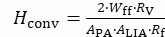 с,
с,
где фактор, который зависит от формы волны модуляции32.
ПРИМЕЧАНИЕ: Для входящих синусоидных волн,
 ; для треугольной
  волны, ; и для квадратной
  волны, . Типичными значениями для измерения тонкопленочных солнечных элементов на
 жестких
 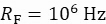 рентгеновских нанозондах являются: , ,
  .
. - Для возможной коррекции необработанного сигнала
 XBIC для топологических вариаций используйте28:
(2) ,
,
с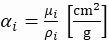 коэффициентом затухания рентгеновского излучения33 и
 плотностью массы для абсорбатора элемента, который может быть измерен с помощью одновременных измерений XRF17.
 - Для возможного преобразования сигнала XBIC в
 эффективность сбора заряда, используйте23:
(3)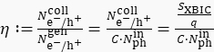 ,
,
где
 и являются генерации и скорости сбора
  электронного отверстия пар,
  является скорость фотонов инцидента, является элементарным зарядом, и
  является постоянным материалом.
 - Для окончательного расчета материала постоянной, использование:
(4)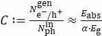 ,
,
где энергия, отложенная в амортизаторе слоя DUT за
  инцидент рентгеновский фотон, является
  диапазоном амортизатора материала, и является постоянной.
ПРИМЕЧАНИЕ: Фактор учитывает энергоэффективность генерации пары электрон-дыр. Это часто приближается23,  34 как .
 - Для окончательной оценки уровня
 впрыска, по сигналу XBIC, используйте:
(5)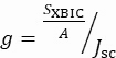 ,
,
где интерпретируется как количество  эквивалентов Солнца, является поперечное сечение рентгеновского луча и
  является плотностью тока короткого замыкания при стандартных условиях измерения35.
- Идите по цепочке сигналов от DUT к единице сбора
Результаты
Ключевым преимуществом использования усиливаем блокировки для измерений XBIC является резкое увеличение соотношения сигнала к шуму по сравнению с измерениями со стандартным усилением. Параметры измерений, которые особенно важны для успешного измерения XBIC, будут обсуждаться в первых пяти разделах. К их мнению: а) модуляция сигналов; b) предварительное усиление; c) смешивание сигналов в ЛИА; d) низкопроходивая частота фильтра ЛИА; e) сворачивание фильтра с низким уровнем прохода в ЛИА.
Иллюстрации воздействия этих параметров показаны на рисунке 3, Рисунок 4, Рисунок 6. Для измерений лабораторная установка использовала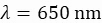 красный лазер () вместо рентгеновского луча, модулированного на
  2177,7 Гц оптическим вертолетом. Флуоресцентные трубки служили источником для предвзятого света. DUT был тонкопленочный солнечный элемент с Поглотителем Cu (In,Ga)Se2 (CIGS). Хотя различные параметры измерения будут выбраны для других DUT, общие руководящие принципы, описанные здесь, чтобы найти подходящие настройки действительны для различных DUT, таких как солнечные элементы с различными слоями поглотителя или нанопроводов. PA был использован с коэффициентом
  усиления . Обсуждаемые здесь эффекты в равной степени применимы и к другим предусилителям. Если ничего не указано, то свертывание фильтра с низким проходом LIA составило 48 дБ/окт.
Следующие разделы (f)-(i) показывают примерные результаты для отображения возможностей и проблем измерений XBIC в сочетании с другими режимами измерения. В (f) обсуждаются конкретные проблемы измерений XBIC в режиме сканирования полетов. В (g), XBIC и XRF измерения солнечного элемента CIGS сочетаются, и эффект блокировки в усиление обсуждается с смещением напряжения применяется. В (h) XBIV добавляется в качестве режима измерения для солнечных батарей CIGS. В (i), XBIC и композиционные данные от XRF нанопровода CdS показаны. Для всех измерений XBIC в разделах (f) к (i), мы использовали PA и LIA как указано в таблице материалов и реагентов.
a) Модуляция входящего сигнала
На рисунке 3 показан предварительно усиленный ответ DUT, измеряемый областью без (верхний ряд) и с включенным (нижним рядом) светом смещения. Когда PA преобразует токи в напряжение, отображаемый сигнал находится в вольтах. Он отрицательный из-за контакта с солнечной батареей, с p- и n-типа контактов, подключенных к щиту и ядро ввода PA, соответственно. В измерениях XBIC, соприкасание солнечных элементов регулируется необходимым заземлением переднего контакта, как это обсуждалось в разделе 1.3.6. протокола.
Сравнивая рисунок 3A и рисунок 3D,мы отмечаем смещение сигнала на порядка 8 мВ, который смещается до -65 мВ, включив свет смещения от флуоресценции труб. Кроме того, изменение сигнала на коротких временных шкалах значительно усиливается уклоном света. Такое смещение смещения примерно 70 мВ может оказаться проблематичным, из-за ограничений в диапазоне принятия PA и LIA. Как мы хотели бы использовать весь спектр PA, небольшое смещение, как в рисунке 3A-C является предпочтительным. Поэтому все источники непреднамеренного смещения, такие как освещение окружающей среды, должны быть устранены.
Добавление измельченного источника фотона, как показанона рисунке 3B,C,E,F, увеличивает индуцированный сигнал на ту же сумму - примерно 66 мВ - как с и без света смещения, когда луч проходит через лопасти вертолета; когда луч блокируется лезвием, сигнал остается на уровне соответствующего смещения, как и ожидалось. Частота вертолета отличается в сигнале Рисунок 3B и 3E с периодом 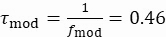 мс.
мс.
На рисунке 3D-Fмы отмечаем дополнительную модуляцию с частотой 90 кГц. Источником этой высокочастотной модуляции является электронный балласт флуоресцентной трубки, который приводится при частоте 45 кГц. Хотя усиление блокировки способно дифференцировать вклады от различных частот модуляции, как будет показано на рисунке 6,снижение шумового сигнала имеет первостепенное значение для хорошего измерения. Ambient свет является лишь одним из возможных источников, но другие электроники могут также вызвать шум, который затем будет накладывается на сигнал. Обратите внимание, что смещение света не всегда нежелательный шум, но часто смещения свет применяется специально, чтобы установить DUT в условиях эксплуатации.
На рисунке 3B,C,E,F, мы отмечаем далее, что реакция DUT на изменение интенсивности облучения задерживается. Эти эффекты подъема времени будут обсуждаться более подробно в следующем разделе и происходят здесь из двух различных эффектов: во-первых, резкое увеличение и уменьшение DUT ответ на 2177,7-Гц модуляции задерживается фильтр низкого прохода в ПА. Во-вторых, сигнал продолжает увеличиваться/уменьшаться в более медленных временных масштабах (например, видим между 0,68 и 0,80 мс на рисунке 3C),что мы приписываем оккупационной кинетике дефектных состояний в солнечной камере.
b) Предварительное усиление
PA не только усиливает модулированный сигнал DUT, но может значительно изменить свою форму волны. Как описано выше, контакты солнечных батарей таковы, что отрицательное напряжение измеряется при освещении. Для измерений, показанных на рисунке 4, не было добавлено предвзятого света.
Измерения были сделаны с увеличением времени подъема фильтра, чтобы продемонстрировать их эффект, когда сила усиления держится постоянно. Во многих случаях время подъема фильтра связано с усилением. Чем сильнее усиление, тем больше время отклика, и чем меньше частота отключения фильтра с низким проходом в PA36,37.
С фильтром время подъема 10 й, как в верхней панели Рисунок 4, сигнал едва задерживается, охватывает номинальный пик до пика диапазоне от примерно 10 мВдо -65 мВ, и достигает плато на пиковых значениях. С 100 й фильтр время подъема, задержки эффекты видны в модулированных сигнала, но модуляция по-прежнему различны и амплитуды находится в том же диапазоне, как для 10 кс. Время подъема фильтра 1 мс больше, чем период модуляции (0,46 мс). Таким образом, модуляция подавляется до амплитуд ниже 10 мВт, и форма отражает только начало восходящего и падающего края, что, очевидно, не подходит для количественных измерений XBIC. Эта связь между усилением и временем роста фильтра должна быть в виду,  особенно для сочетания частот быстрой модуляции, с сильным усилением.
c) Смешивание сигналов
Ключевым отличием стандартного усиления сигнала и усиления блокировки является смешивание сигнала DUT с помощью эталонного сигнала и последующее подавление высоких частот фильтром с низким проходом.
Путь сигнала для смешивания изображен на рисунке 5. Для обсуждения смешивания сигнала, несколько упрощений сделаны. Сигнал эталона можно охарактеризовать как синусоидальный сигнал
(6)  ,
,
где  находится амплитуда и
  частота модуляции эталонного сигнала. Модулированный сигнал DUT, подаваемого в LIA, может быть представлен таким же образом, как
(7)  ,
,
где  амплитуда
  и является частотой модуляции
  сигнала DUT, и является фазовой смещением сигнала DUT к сигналу ссылки.
Исходя из (1) и (2), смешанный сигнал:
(8)  .
.
Частота модуляции DUT является  эталонной частотой, . Таким образом, тригонометрический принцип
(9)
может быть использован  для переписывания в качестве суммы двух терминов с различными частотами:
(10)  .
.
 Фильтр с низким проходом смягчает быстрый сигнал таким образом, что усиленный сигнал блокировки может быть приближен38,39 как
(11)  .
.
Сигнал DUT, смешанный с эталонным сигналом, называется вфазным компонентом, а сигнал DUT, смешанный с 90-фазной ссылкой, называется компонентом квадрататуры:
(12)
(13)  .
.
От Эк. (12) и (13), амплитуда RMS
(14)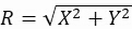
а также фазы
(15)
смешанного сигнала может быть получен с помощью касательной функции arcus с двумя аргументами. Многие ЛИА имеют внутреннюю фазу, приспосабливающуюся к нулю во время измерений.
d) Низкочастотная частота фильтров
На рисунке 6 показан эффект смещения света и различных низкопроходимых параметров фильтра на усиленную амплитуду RMS. Мы использовали LIA, что позволило нам записывать сигнал, полученный от различных параметров фильтра одновременно.
Частота  отсечения фильтра с низким проходом определяет частоту, при которой сигнал смягчается до 50%. В то время как нижние частоты передаются, более высокие частоты подавляются. Рисунок 6A,E показывает прямой сигнал с 466,7 кГц, который эффективно не устраняет шум или низкочастотные модуляции, но позволяет им проходить с необработанным сигналом. Преобразование сырого предварительно усиленного сигнала в амплитуду RMS приводит к дополнительному фактору для частот достаточно ниже. Например, постоянное
  вхожжье
  напряжение вывода как .
В то время как средняя смещение на рисунке 6E является незначительным без смещения света (в среднем 2 мВ), она увеличивается в среднем около 75 мВ с предубеждением света(рисунок 6A). Разница сопоставима, как между рисунком 3A и рисунок 3D, но будьте осторожны, что это были отдельные измерения. В обоих случаях включение источника измельчения приводит к значительному увеличению, а пиковое изменение соответствует пиковому изменению необработанного сигнала, показанного на рисунке 3B и рисунке 3E .
На рисунке 6B,F, амплитуда RMS отображается после использования фильтра с низким проходом с  1000 Гц. Опять смещение можно наблюдать в Рис 6B из-за света смещения, но смещение более мало с вокруг 18 mV на среднем. Это смещение вызвано модуляцией флуоресцентного света в 100 Гц, в то время как модуляция 90 кГц блокируется фильтром с низким проходом. Кроме того, уровень шума в состоянии «луч на» по-прежнему значителен с пиковым и пиковым изменением около 46 мВ, в то время как среднее значение сигнала составляет 32 мВ. Без предвзятого света(рисунок 6F) пик-пик овое изменение составляет около 17 мВт во время "луч на" со средним значением 23,5 мВ. Среднее смещение во время «отключаемого луча» меньше 0,5 мВ.. Эти измерения показывают, что сочетание фильтра с низким проходом с 1000 Гц и частотой измельчения 2177,7 Гц не является идеальным: сигнал, несущий частоту модуляции, удаляется лишь частично, но не полностью подавляется низкопроходным Фильтр. Оставшаяся часть приводит к значительным пиковым колебаниям во время состояния «луч на». При предвзятом свете модуляция 100 Гц благодаря чистой частоте флуоресценционных ламп еще больше увеличивает значения пика к пику.
На рисунке 6C,G, влияние смещения света можно рассматривать как минимальный: 10,27 Гц низкопроходной фильтр отрезает большинство шума и модуляции флуоресцентного света, и четкий луч индуцированных сигнал может быть извлечен. Хотя едва заметны здесь, смещения и распространения шума по-прежнему немного больше с уклоном света. Это может быть вызвано бродячих свет, проходящий через колесо вертолета на DUT. Поэтому рекомендуется внедрить вертолет далеко вверх по течению, чтобы избежать модуляции рассеянного света.
Рисунок 6D,H — это масштаб изменения от «лучна на» до «отключать» после 6 с на рисунке 6B,C,F,G,соответственно. Наложенная модуляция на 100 Гц (частота флуоресценции ламп) видна на рисунке 6D для фильтра с низким проходом с 1000 Гц. Обратите внимание также на задержку сигнала после фильтра с 10,27 Гц по сравнению с сигналом после фильтра с 1000 Гц, когда луч выключен. Подобно тому, как в случае медленного подъема время PA, низкий фильтр низкого прохода в LIA вызывают более медленную адаптацию к изменениям сигнала.
В общей сложности, мы обнаружили, что фильтр с низким проходом с 10,27 Гц и откат 48 дБ/окт (см. следующий раздел) предлагает в этом случае лучший компромисс между быстрой скоростью сканирования (в пользу высоких значений) и подавлением смещения света или шума (в пользу низких значений, самое главное ниже сетки частоты 50 Гц).
e) Скатфильтра с низким проходом
Как и многие цифровые усилители блокировки, модель, которая была использована здесь использует так называемые дискретные время RC фильтры или экспоненциальные работает средний фильтры, характеристики которых очень близки к аналоговым резистор-конденсатор RC фильтр40. Помимо частоты отсечения фильтра, которая обсуждалась в предыдущем разделе, есть только один свободный параметр, порядок  фильтра, который определяет наклон отсечения как
  dB/oct.
Рисунок 7A показывает влияние порядка фильтра на частотно-зависимое затухание для различных частот отсечения, которые соответствуют константам времени  ms и
ms и  ms. Time константы между этими двумя крайностями подходят для большинства XBIC Измерения. Затухание фильтра было рассчитано40 в области
  частоты как абсолютное значение квадратное функции сложной передачи
(16)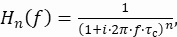
как функция частоты  и фильтр порядка с
  постоянным временем. Функции передачи фильтров более высокого порядка приобретаются путем умножения функций передачи последовательно подключенных отдельных фильтров. Подобно
 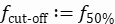 , мы
, мы 
 определяем и как частоты, на которых затухания составляет 5% и 95%, соответственно. Продукт этих частот и
  является постоянным и дается в таблице 1 для преобразования между частотами отсечения и постоянное время фильтра.
В домене времени,  ответ
ответ  фильтра для recursively
  вычисляется от сигнала
 вхоза который определен на дискретных временах,,,
  etc., помещенном временем
  выборки:
(17)
Ответ фильтров с  рассчитывается по нескольким итерации Eq. 17 с
  рассчитанным от
 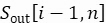 и
и 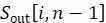 . Реакция фильтра на увеличение (в момент 0) и
  уменьшающуюся функцию шага (в данный момент) отображается на рисунке 7B для заказов фильтров от 1 до 8, как функция времени в единицах . Обратите внимание, что ответ задерживается в отношении ввода сигнала и что эта задержка увеличивается с . Задержка количественно в таблице 1, как
 раз,
раз,  и , в течение которого передаваемый сигнал достигает 5%, 50%, или 95%, соответственно.
Выбор правильного свертывания фильтра так же критичен, как и частота отсечения при проектировании эксперимента. В приложении 1 представлено в разделе (g), высококачественные измерения XBIC были получены с частотой измельчитель 1177 Гц, время пребывания 100 мс, и частота отсечения 40 Гц на фильтре порядка 8. С числами из таблицы1  ,
,  это переводится как , и . Это время значительно короче, чем время пребывания, так что никаких задержек артефакты не вводятся.
f) Коррекция времени
В классических измерениях ступенчатого режима этап сканирования перемещается в номинальное положение, и начало измерения в этом пиксельном положении срабатывает после достижения точного положения. Для коротких времени, время оседания становится ограничивающим для общего времени сканирования, что мотивирует так называемые мухи-сканирования или непрерывного измерения режимов: там, этап сканирования движется непрерывно, и данные измерения отнесены к пикселям с закодированным стадии в пост-обработке. Однако это может привести к дополнительным проблемам, как показано на рисунке 8. В этом случае двигатели сцены выборки не двигались равномерно в направлении, в результате чего разное время проложа в пикселе (см. рисунок 8А). Вариации времени пребывания непосредственно переводят на вариации измерений XBIC, как видно на рисунке 8C. Поэтому сигнал XBIC должен быть нормализован к времени пребывания, результаты которого показаны на рисунке 8D. Аналогичным образом, изменения интенсивности луча (отображаются на рисунке 8B)часто должны учитываться путем нормализации потока фотонов. Сигнал XBIC нормализован ный с потоком фотона можно увидеть на рисунке 8E; для минимальной ошибки на абсолютной количественной оценке XBIC, сам поток фотонов был нормализован к его медианному значению. На рисунке 8F показана карта XBIC, нормализованная для времени, так же как и для потока фотонов, что уменьшило воздействие большинства артефактов измерения. Наконец, на рисунке 8G показаны данные XBIC после преобразования от счета к текущей с использованием Eq. (1).
g) Применение 1: XBIC солнечной ячейки с напряжением предубеждений и XRF
На рисунке 9A-B показано влияние усиления блокировки на соотношение сигнала к шуму в рентгеновских измеряемых токовых измеряях. Шум прямого сигнала очевиден на рисунке 9A:сильные контрасты интенсивности от строки к линии свидетельствуют об артефактах измерения, а тонкие вариации XBIC из DUT закапываются в произвольно меняющийся сигнал. С другой стороны, эти тонкие черты хорошо видны на рисунке 9B. Обратите внимание, что уровень шума на рисунке 9A необычайно высок по неизвестным причинам, несмотря на оптимизацию установки до измерений. В таких случаях улучшение соотношения сигнала к шуму путем усиления блокировки значительно выше, чем в случаях уже высокого соотношения сигнала к шуму со стандартным усилением (например, применение 3 в разделе (i)), где усиление блокировки будет только привести к незначительным улучшениям.
С PA, вперед(рисунок 9C) и обратный (рисунок9D) смещения напряжения -50 мВ и 50 мВ, соответственно, были применены к образцу и области Рисунок 9A-B отсканированы. Доминирующие черты, видимые на рисунке 9B, по-прежнему видны на рисунке 9C и рисунке 9D,но они менее различны, так как карты более шумные. Это потому, что применение смещения напряжения или смещения света вызывает прямой ток, который часто порядки больше, чем модулированный сигнал XBIC. В конечном счете, соотношение прямого к модулированному сигналу ограничивает применимость усиления блокировки. Несмотря на плохое соотношение сигнала к шуму, стоит отметить, что усиление блокировки позволяет отображение производительности солнечных батарей на наноуровне с припадковым напряжением и смещением света, что вряд ли было бы возможно в противном случае30.
Поскольку производительность ciGS солнечных батарей коррелируетс составом слоя амортизатора 7,41, мы измерили сигнал XRF одновременно с XBIC. На рисунке 9E-F, концентрации Га и Ин представлены. Оба элемента являются частью слоя амортизатора и их соотношение считается большим влиянием на производительность солнечных батарей7. Статистика Ga гораздо больше, чем для In, что связано с более высоким коэффициентом поглощения и менее самопоглощения при возбудительской энергии 10,4 кэВ. Из-за низкой статистики, особенности на карте In почти невидимы, в то время как концентрация Ga достаточно ясна, чтобы быть коррелированным с электрической производительностью на рисунке 9B. Для более высокого В сигнале, одно смогло или выбрать более длиннее время dwell или выбрать энергию поглощения с более большим В сечении поглощения. Это иллюстрирует важность достаточно длительного пребывания в течение времени, а также адаптации энергии луча к элементам, представляющим интерес.
С длинными временами пребывания и большими картами, другой момент должен иметь в виду: во время измерений, охватывающих несколько часов, выборка дрейф может стать критической проблемой. Тепловые колебания (особенно после изменения образца или больших движений двигателя с плохим рассеиванием тепла) и нестабильность компонентов механической стадии часто приводят к дрейфу образцов, как это видно, сравнивая вертикальные позиции Рисунок 9D и Рисунок 9B.
h) Применение 2: XBIC солнечной ячейки с XBIV и XRF
На рисунке 10 показано мультимодальное сканирование солнечного элемента CIGS, где ячейка работает в условиях короткого замыкания, измеряя XBIC на рисунке 10A,и под состоянием открытого замыкания, измеряющим XBIV на рисунке 10B. Измерение XRF, показанное на рисунке 10C, было проведено одновременно с измерением XBIV. Чтобы собрать достаточное количество XRF, время пребывания на пиксель составило 0,5 с для рисунка 10B-C по сравнению с 0,01 с на рисунке 10A. Соответственно, более низкая частота отсечения в фильтре с низким проходом для измерения XBIV может быть использована по сравнению с измерением XBIC (10,27 Гц против 501,1 Гц, оба с свертыванием 48 дБ/окт). Только для измерений XBIV мы могли бы использовать те же параметры продезы и низкопроходившие настройки фильтра, что и для измерения XBIC с аналогичным соотношением сигнала к шуму. Тем не менее, было в целом более эффективным по времени сочетать XBIV с измерениями XRF с измерениями XRF, регулирующими время пребывания, чем выполнение отдельных измерений XBIV и XRF.
Сравнивая Рисунок 10A, и рисунок 10  B, мы отмечаем, что короткое замыкание тока , измеряется как XBIC, и открытое напряжение цепи
  , измеряется как XBIV, коррелируются: большие высокие и низкопроизводительные области видны в обоих режимов измерения. Это указывает на то, что локальные вариации толщины и/или рекомбинации доминируют в производительности здесь, а не вариации бандапа, что приведет к противоположным тенденциям в XBIC и XBIV28.
Кроме того, принимая во внимание рисунок 10C, можно  увидеть, что некоторые области с низкой производительностью, такие как в коррелирует с низким cu рассчитывать скорость, в то время как производительность не коррелирует с Cu кол-считать в других областях.
i) Применение 3: XBIC и XRF nanowire
Помимо солнечных батарей, контактированные нанопровода24 или нано-листы, а также квантовые точки, являются другими примерами DUT, которые могут получить прибыль от блокировки в усиленных измерениях XBIC. Для демонстрации на рисунке 11А показано элементарное распределение измерений XRF, а на рисунке 11B - соответствующая карта XBIC нанопровода CdS. Два контакта, сделанные из Pt и cdS провода четко различимы, и сигнал XBIC показывает соответствующий электрический ответ. Особенно примечателен тот факт, что XBIC может раскрыть электрическую производительность нанопровода под контактом Pt, который уникален для рентгеновских нанозондов и связан с высокой глубиной проникновения жестких рентгеновских лучей. Дополнение материального состава и электрических свойств нанопровода образцово демонстрирует преимущества мультимодальных рентгеновских измерений.
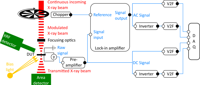
Рисунок 1 : Настройка для блокировки усиленного рентгеновского луча индуцированных тока (XBIC) измерений на устройстве, наиболее тестируемом (DUT). Путь луча изображен красным цветом. Зеленые формы указывают на факультативную рентгеновскую флуоресценцию (XRF) и детекторы области для мультимодальных измерений, желтый указывает на факультативный свет смещения. Компоненты оборудования для измерений XBIC окрашены в черный цвет, в то время как пути сигнала XBIC синие с сигнальными выходами и входными сигналами, показанными как заполненные и пустые круги, соответственно. Перед получением данных (ДАЗ) сигнал DC (прямой ток) и ac (переменный ток) преобразуется из напряжения в частоту (V2F). Для альтернативных путей сигнала мы ссылаемся на часть a) раздела обсуждения. Пожалуйста, нажмите здесь, чтобы просмотреть большую версию этой цифры.
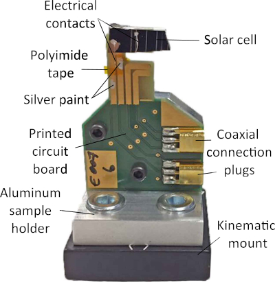
Рисунок 2 : Пример кинематический образец держателя оптимизирован для мультимодальных рентгеновских измерений микроскопии, включая рентгеновский луч индуцированного тока. Тонкие медные провода устанавливаются на передние и задние контакты солнечной ячейки Cu(In,Ga)Se2 (CIGS) с серебряной краской и соединены с контактами ПХД. Полиимидная лента используется для разделения проводов, избегая короткого замыкания образца. Пожалуйста, нажмите здесь, чтобы просмотреть большую версию этой цифры.
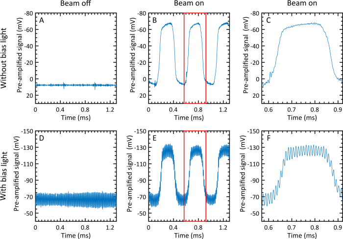
Рисунок 3 : Предварительно усиленная реакция солнечных батарей при облучении с уклоном света и модулированного луча. Верхний ряд без предвзятого света, нижний ряд с уклоном света: A и D - луч off; B и E - луч на; C и F - увеличить в красный прямоугольник B и E. Пожалуйста, нажмите здесь, чтобы просмотреть большую версию этой фигуры.
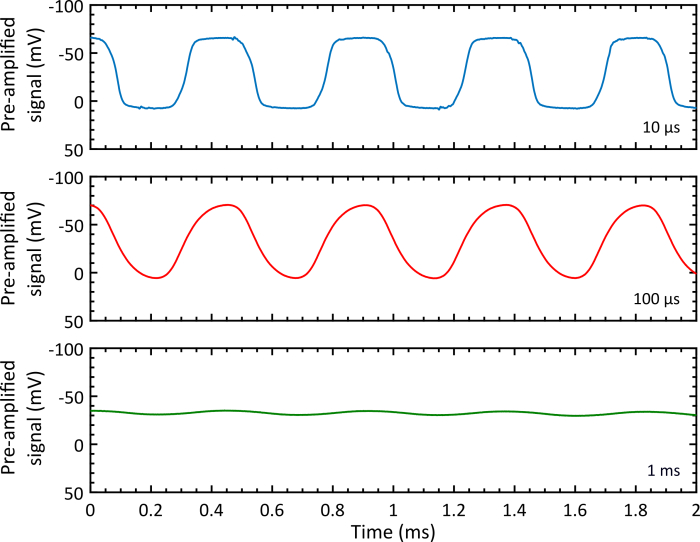
Рисунок 4 : Реакция солнечных элементов после предварительного усиления с тремя различными временами подъема фильтра (10 - синий, 100 - красный, 1 мс - зеленый) в предварительном усилителе. Пожалуйста, нажмите здесь, чтобы просмотреть большую версию этой цифры.
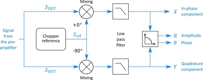
Рисунок 5 : Обработка сигнала усилителем31.  является вхотворемым
  сигналом от DUT и является эталонным сигналом отвертолета. Пожалуйста, нажмите здесь, чтобы просмотреть большую версию этой цифры.
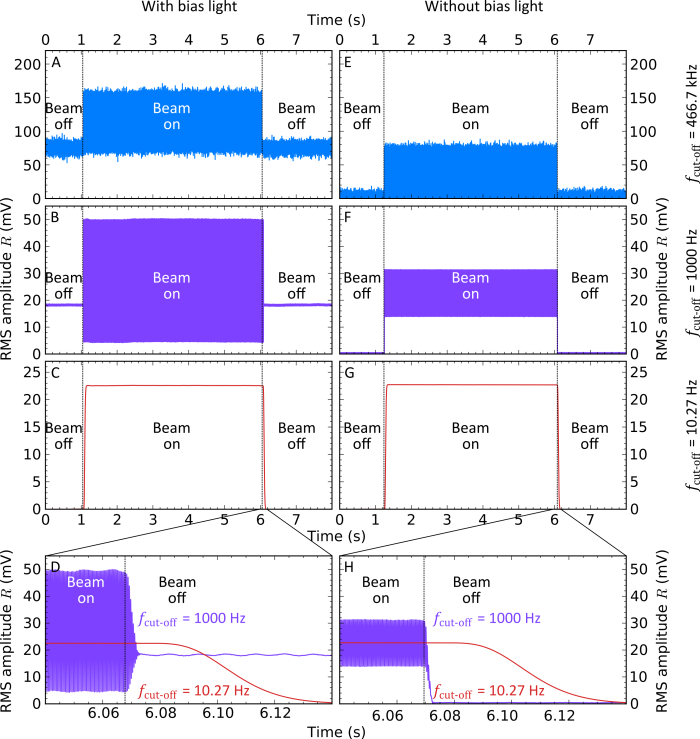
Рисунок 6 : Блокировка в усиленной амплитуда RMS с низкопроходимыми частотами  отключения фильтра 466,7 кГц (синий), 1 кГц (фиолетовый), 10,27 Гц (красный) и постоянным сворачиванием фильтра 48 дБ/окт. DUT был Cu (In,Ga)Se2 солнечные батареи с (A, B, C, D) и без (E, F, G, H) смещения света применяется. Времена, когда нарезанный фотонный луч был включен и выключен, указаны в цифрах как вертикальные линии. Пожалуйста, нажмите здесь, чтобы просмотреть большую версию этой цифры.
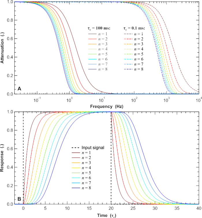
Рисунок 7 : Эффект низкопроходимых параметров фильтра в усилителе блокировки. A - Затусание фильтром с низким проходом в частотном домене в течение двух временных констант (мс и мс) и для заказов фильтров от 1 до 8. B - Передаваемая реакция сигнала фильтра низкого прохода в домене времени, в блоках времени постоянная, для заказов фильтра 1 до 8 на шаг-как изменение входного сигнала от 0 до 1 в времени 0 и от 1 до 0 в времени. Пожалуйста, нажмите здесь, чтобы просмотреть большую версию этой цифры.
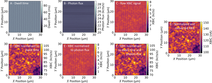
Рисунок 8 : Fly-сканирование измерения Cu (In,Ga)Se2 солнечных батарей на луч P06 на PETRA III, принятые в 15,25 кеВ фотона энергии с целенаправленным потоком около  ph/s. PA был использован
  с No 106 V / A, и ЛИА с
  Гц (48 дБ/окт). A - время пребывания, B - фотонный поток, C - рентгеновский луч индуцированного тока (XBIC); Карта XBIC нормализовалась до: D - время пребывания, E - поток фотона нормализованный до его медианного значения, F - время пребывания и нормализованный поток фотона. G - нормализованный сигнал XBIC после преобразования от счета к текущему с использованием Eq. (1). Пожалуйста, нажмите здесь, чтобы просмотреть большую версию этой цифры.
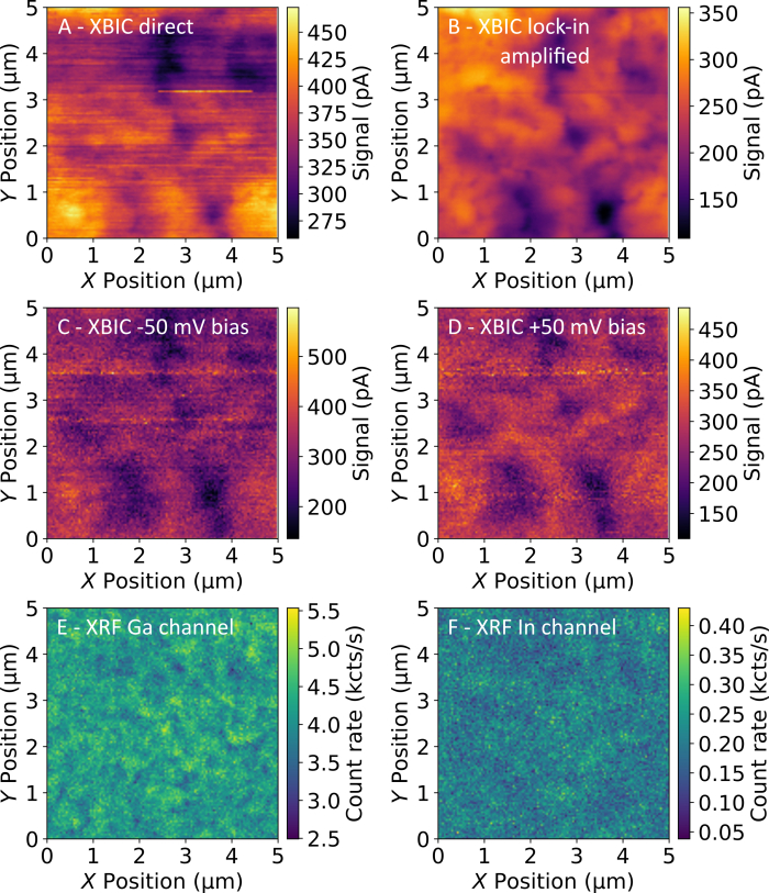
Рисунок 9 : Рентгеновский луч индуцированного тока (XBIC) и рентгеновской флуоресценции (XRF) измерения Cu (In,Ga)Se2 солнечных батарей, принятых на лучевой линии ID16B в Европейском синхротронном радиационном комплексе с сфокусированным потоком на заказ  ph/s. PA был использован
  с V /
с V /  A, LIA с Гц (48 дБ/октябрь). Энергия луча составила 10,4 кэВ, частота измельчительов - 1177 Гц, а фильтр с низким проходом отрезан на 40 Гц. Время пребывания было 100 мс, а размер пикселя - 40 нм х 40 нм. Карты A, B, E и F были сделаны одновременно; C и D перебираются после 50 мин и 113 мин, с 50 мВт вперед и обратное напряжение смещения применяется, соответственно. Пожалуйста, нажмите здесь, чтобы просмотреть большую версию этой цифры.
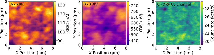
Рисунок 10 : Мультимодальное измерение Cu (In,Ga)Se2 солнечных батарей, принятых на луч P06 на PETRA III с целенаправленным потоком около ph/s. Энергия луча составила 15,25 кэВ, частота измельчительов - 8015 Гц, размер пикселей - 50 нм х 50 нм. A - рентгеновский луч индуцированного тока (XBIC), измеренного с временем пребывания 0,01 с, PA с 106 V/A и ЛИА с  Гц (48 дБ/октябрь); B - рентгеновский луч индуцированного напряжения (XBIV), охватывающий ту же область, что и панель
  А, измеренная с временем пребывания 0,5 с и ЛИА с Гц (48 дБ/октябрь); C - Cu колеи от рентгеновского флуоресценции (XRF) измерения, принятые одновременно с измерением XBIV. Пожалуйста, нажмите здесь, чтобы просмотреть большую версию этой цифры.
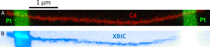
Рисунок 11 : Мультимодальное измерение нанопровода CdS с контактами Pt, сделанное на луче 26-ID-C расширенного фотонного источника с энергией луча 10.6 keV. A - Распределение Pt и Cd от измерения рентгеновской флуоресценции. B - рентгеновский луч индуцированного тока (XBIC) измерения, сделанные одновременно с измерением XRF, без усиления блокировки. Пожалуйста, нажмите здесь, чтобы просмотреть большую версию этой цифры.
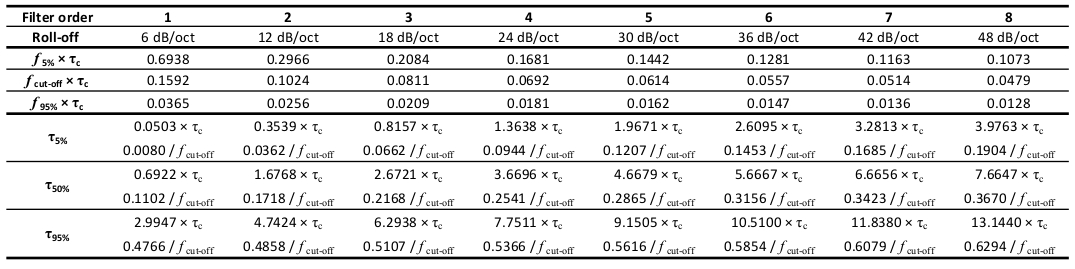
Таблица 1: Для дискретных RC фильтров заказов от 1 до 8, продукт времени постоянной и частоты, при которой сигнал ослаблен на 5% (), 50% ( ,
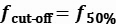 и 95% ( ),
 является постоянным и дается в верхнейчасти . В нижней части дается задержка времени, в течение которойсигнал достигает5% (),50% (), и 95% (),
  в единицах времени постоянной и обратной частоты отсечения. Пожалуйста, нажмите здесь, чтобы скачать этот файл Excel.
| XBIC | EBIC | LBIC | |
| Мультимодальные возможности | ++ | + | + |
| Пространственное разрешение | ++ | ++ | - |
| Глубина проникновения | ++ | -- | + |
| Доступности | -- | - | + |
| Повреждение образца | - | -- | ++ |
Таблица 2: Квалификационная оценка рентгеновского луча индуцированного тока (XBIC), электронного луча индуцированного тока (EBIC) и лазерного луча индуцированного тока (LBIC).
Обсуждение
В этой главе мы сначала обсудим актуальность общих настроек измерения XBIC в отношении шума (а) и скорости сканирования (b). Далее мы помещаем измерения XBIC в контекст мультимодальных измерений и обсуждаем аспекты искусственного повреждения рентгеновского луча (c) и конкретные проблемы, связанные с одновременными измерениями нескольких параметров (d). Наконец, мы сравниваем измерения XBIC с соответствующими измерениями с использованием электронных и лазерных лучей в качестве зондов (e).
а) Шум и ошибка
Хотя усиление блокировки обеспечивает более высокое соотношение сигнала к шуму по сравнению с прямым усилением, крайне важно избегать введения шума на всех уровнях, как это неоднократно подчеркивалось на протяжении всей этой рукописи. Для дальнейшего обсуждения мы ссылаемся на литературу, обсуждая измерение малых электрических сигналов42,43,44,45. Хотя современные усилители блокировки сегодня основаны на обработке цифровых сигналов, большинство стратегий по снижению шума с помощью аналоговых усилителей блокировки по-прежнему применяются.
Резюмируя, следует иметь в виду, что кабели склонны выступать в качестве антенн и тем самым ввести шум в систему. Это особенно верно в среде рентгеновских нанозондов, где сильные электромагнитные поля часто неизбежны, их источники могут даже оставаться неизвестными. Как следствие, кабели должны храниться как можно короче и ориентироваться таким образом, чтобы индуцированный уровень шума был сведен к минимуму. Дополнительная защита сигнальных кабелей может еще больше снизить уровень шума.
Правильный контакт DUT не менее важен для минимизации шума. Чистый и надежный метод с небольшими контактными точками – это связь проводов. Для Солнечных элементов TF, это не всегда работает из-за проблем с адгезией. Кроме того, проводящая лента на основе графита, меди или алюминия подходит для более крупных образцов. Во многих случаях, лучшие результаты получены с ручным применением серебряной краски для контакта тонкой меди, золота или платины проводов к устройству. В то время как лента и графитовая паста не может дать лучший контакт, серебряная краска может легко короткого замыкания устройства и должен быть сдан на хранение с максимальной осторожностью. Полиимидная лента может быть использована для предотвращения короткого замыкания переднего и задней связи.
Обратите внимание, что макет кабелей от контакта к сигнальным транспорту должен быть адаптирован к условиям границы, специфическим для луча. Например, макет, изображенный на рисунке 1 с предварительно усиленным сигналом, разделенным на ЛИА и преобразователями V2F, является рискованным, если преобразователи V2F расположены за пределами загона. В этом случае длинный кабель между преусилителем и преобразователем V2F может уловить шум, который передается в LIA. Таким образом, мы различаем три случая общих сигнальных путей для измерений XBIC или XBIV:
Дело A: XBIC измеряется с помощью предварительного усилителя, а сигнал DC/AC делится после PA, как показано на рисунке 1. В этом случае ток-смещение может быть применено в PA таким образом, чтобы сигнал всегда был положительным, избегая необходимости записи положительного и отрицательного сигнала через два отдельных преобразователя V2F. В качестве недостатка это позволит уменьшить доступный диапазон принятия напряжения в LIA и привести к снижению чувствительности.
Дело B: Избегая разделения предварительно усиленного сигнала, который является только вводом в LIA, дополнительный демодулятор может быть использован в LIA с фильтром низкого прохода на максимальном значении(т.е. не блокировки в частоту модуляции), так что предварительно усиленный сигнал может быть эффективно выводится в блок ДАЗ, как показано на рисунке 6A,E. В этом случае смещение напряжения на выходе может быть применено как к сигналу переменного тока, так и к сигналу ПОСТОЯННОГО тока, избегая необходимости записи положительного и отрицательного сигнала с помощью двух отдельных преобразователей V2F. Это не имеет серьезных недостатков, кроме сокращения доступного диапазона частот V2F, который редко ограничивается.
Дело C: XBIV измеряется и сигнал DC/AC делится между DUT и усилителем блокировки. В этом случае, не смещение напряжения на сигнал е-кете может быть применено без применения нежелательного напряжения смещения на DUT, так что всегда два отдельных преобразователя V2F необходимы для положительных и отрицательных частей сигнала.
Во всех случаях, когда отрицательные и положительные части сигнала регистрируются с помощью двух различных преобразователей V2F, общий сигнал XBIC или XBIV получается как разница между положительным и отрицательным каналом. Если доступна ЛИА с двумя или более демодулаторами, мы обычно предпочитаем случай B, так как он сводит к минимуму проводку необработанного сигнала и позволяет легко переключаться между измерениями XBIC и XBIV.
Ошибка измерений XBIC сильно зависит от используемого оборудования и параметров, что не может быть дано здесь количественной оценки ошибок. Абсолютная ошибка выше, чем можно было бы ожидать из-за экспериментальных и систематических ошибок. Это особенно верно, если сигнал XBIC преобразуется для повышения эффективности сбора путем масштабирования с константой, как описано в протоколе. Например, эмпирическая связь между энергией полосы и ионизации, описанная q (см. Eq. 4), страдает от значительного рассеяния; измерения фотон-потока часто недоступны с абсолютными ошибками ниже 10%; и наноскопическая структура DUT плохо известна. Тем не менее, мы подчеркиваем, что сила блокировки в усиленных XBIC и XBIV измерений заключается в большой относительной точности в картах или сопоставимых измерений.
b) Скорость сканирования
Во многих режимах измерения, основанных на обнаружении фотонов, таких как XRF или рассеяние рентгеновских лучей, интенсивность сигнала увеличивается в первом приближении линейно со временем приобретения, с соответствующим увеличением соотношения сигнала к шуму. Это не относится к измерениям XBIC, где окно возможных скоростей сканирования продиктовано не статистикой подсчетов, а более сложными соображениями, такими как динамика носителя и структура устройства.
Тем не менее, медленные измерения со многими периодами модулированного сигнала на пиксель обычно приводят к наилучшему соотношению сигнала к шуму в усиленных измерениях XBIC, а также к перевыборке с разглаживанием во время постобработки (например, путем нанесения связок или применения фильтры) может еще больше снизить уровень шума, если позволяет время измерения. Однако, помимо соображений пропускной связи, дальнейшие ограничения могут устанавливать более низкие пределы скорости измерения, включая: (1) рентгеновское лучевое индуцированное деградацию (см. следующий раздел) или изменения образца, вызванные окружающей средой, во время на месте измерения часто уменьшают допустимое время пребывания. (2) Выборы дрейфа и воспроизводимости сценических движений могут быть ограниченными, особенно для измерений на наноуровне. (3) Вариации уровня электромагнитного шума могут быть обогнать более быстрыми измерениями. (4) В то время как фотон-счет измерений может быть легко нормализована к инциденту фотон поток, сигнал XBIC (и тем более сигнал XBIV) только в некоторой степени линейной инцидента фотон поток28. Таким образом, нормализация к потоку фотонов компенсирует лишь часть эффектов от изменения фотон-потока, и следует избегать измерения XBIC (например, карты или временные ряды), в то время как поток изменяется. Это особенно проблема, когда кольцо хранения заполняется во время карты XBIC.
Если скорость измерения XBIC не регулируется другими режимами измерения (см. раздел (d)), измерения XBIC обычно проводятся с максимальной скоростью, которая обеспечивает удовлетворительное соотношение сигнала к шуму. Верхние пределы скорости измерения даются следующими ограничениями: (1) Фундаментальным верхним пределом скорости измерения является время отклика DUT. В конечном счете, время отклика ограничено временем сбора заряда. Для большинства тонкопленочных солнечных элементов с сроком службы заряда-носителя в диапазоне нано- или микросекунд это некритично, но это необходимо иметь в виду для высококачественных кристаллических кремниевых солнечных элементов со сроком службы в несколько миллисекунд. Тем не менее, эффекты емки могут увеличить время отклика также TF солнечных элементов, таким образом, что он может ограничить скорость измерения. (2) Вращающиеся лопасти вертолета, которые используются для модулирования рентгеновского луча, имеют верхние ограничения скорости. В зависимости от их расположения в рентгеновском луче размер луча может быть до 1 мм в ширину, что определяет минимальный период клинка. Если вертолет работает в вакууме, частота вращения редко ограничивается, что в некоторых случаях даже частота электронов. Тем не менее, работа вертолетов на таких скоростях в вакууме является сложной задачей, так что большинство вертолетов работают в воздухе. В этом случае скорость вращения ограничена механическими вибрациями и, в конечном счете, скоростью самой высокой части лезвия, которая должна быть меньше скорости звука. По нашему опыту, частота измельчения часто ограничивается 7000 Гц в воздухе. (3) Во многих случаях время отклика ПА устанавливает верхний предел скорости измерения. Как показано на рисунке 4, быстрое время подъема PA требуется для перевода модуляции сигнала с вертолета. Для большого усиления используются усилители тока низкого уровня шума, которые имеют время подъема до 100 мс. При таком времени подъема частота измельчения может быть ограничена несколькими Гц, что потребует времени проветривания в несколько секунд. Таким образом, лучшая стратегия часто выбрать более низкое усиление ПА с более быстрым временем отклика, который соответствует частоте измельчения. Хотя это приводит к меньшему уровню сигнала к шуму после предварительного усиления, усиление блокировки часто может по-прежнему получать высококачественный модулированный сигнал.
В качестве примера, используемый PA обеспечивает пропускную способность более 10 кГц для усиления в диапазоне ЗА / V, даже для низкого шума настройки37. Это позволяет измельчения в диапазоне кГц и измерения скорости до 100-Гц диапазон с низким проходом фильтр аттестунок с частотой отсечения между сканированием и измельчения частоты. Это условия измерения, которые мы часто используем.
Чтобы избежать артефактов измерения, крайне важно проанализировать сигнал по цепочке усиления: в то время как ограничение фильтром с низким проходом LIA может быть легко обнаружено в виде линейных артефактов на картах (размазывание сигнала XBIC по нескольким пикселей), системный ответ DUT и PA требует осмотра сигнала по объему, который может быть интегрирован в LIA.
c) Повреждение балки
Рентгеновский луч индуцированных повреждений является общей проблемой и был обсужден для многих систем, от биологических образцов кремниевых солнечных элементов и детекторов46,47. Хотя неорганические полупроводники, как правило, более надежны против рентгеновского облучения по сравнению с органическими полупроводниками или биологическими системами, рентгеновский луч индуцированных повреждений является общим также в тонкопленочных солнечных элементов. В частности, мы наблюдали рентгеновский луч индуцированных повреждения солнечных элементов с CdTe, CIGS29, перовскит18, и органических слоев поглотителя. Обратите внимание, что электронная реакция DUT, как солнечные батареи чувствительна к концентрации дефекта ниже уровня ppm, где заряд-носителя рекомбинации влияет на производительность без видимых химических повреждений.
Таким образом, как правило, требуется проверить чувствительность DUT к повреждению пучка. На практике мы оцениваем рентгеновскую пучковую деградацию любого DUT до фактических измерений XBIC и устанавливаем условия, позволяющие измерениям в наименьшей степени подвержены влиянию последствий деградации.
Существуют различные стратегии, чтобы справиться с рентгеновским лучом индуцированного повреждения, но все они имеют в общем то, что они направлены на снижение дозы излучения в месте измерения до оценки производительности там. Другими словами, цель состоит в том, чтобы обогнать деградацию после парадигмы "мера быстрее, чем DUT деградирует". Стратегии включают в себя: (1) Использование коротких раз, но в них. (2) Увеличьте размер шага, уменьшая разрешение измерения. (3) Уменьшить интенсивность рентгеновского луча путем затухания фильтров. В зависимости от линии луча и DUT могут быть выбраны различные подходы или их комбинация. Например, отсутствие быстрых ставней или режимов сканирования мух исключают (1), а широко распространенные профили рентгеновских лучей, такие как профили, генерируемые зональных пластинами, могут привести к значительной деградации вдали от положения центрального луча.
К счастью, большинство механизмов деградации приводят лишь к локальному усилению рекомбинации носителя заряда. Это ограничивает боковое воздействие деградации на диффузионную длину носителей заряда, а измерения XBIC дальше от деградированных районов остаются почти не затронутыми. Если вместо этого механизмы деградации приведут к локальному шунтированию ДУТ, дальнейшие измерения XBIC будут серьезно затруднены. Чтобы свести дозировку отложенного излучения к минимуму, критические измерения должны быть выполнены сначала на свежем месте, а затем, фотон-голодные методы, такие как XRF, которые более равнодушны к повреждению пучка, могут быть использованы в том же месте.
d) многомодальности
Совместимость XBIC с режимами дальнейшего измерения обеспечивает прямую точечную корреляцию электрической производительности с одновременно оцениваемыми параметрами23. Здесь мы кратко обсудим сочетание измерений XBIC с измерениями XBIV, XRF, SAXS, WAXS и XEOL. Сочетание с дальнейшими режимами измерения, такими как выход электронов или голография, можно легко представить, но эти режимы, как правило, не совместимы с настройками или режимами сканирования измерений.
Даже если возможно геометрическое расположение детекторов и образцов для одновременного измерения XBIC, XBIV, XRF, SAXS, WAXS и XEOL, существуют фундаментальные и практические аспекты, запрещающие одновременную оценку всех режимов.
(1) Состояние солнечных батарей запрещает одновременные измерения XBIC (короткая цепь) и XBIV (открытое замыкание) измерений. Как XEOL48,49 меры радиационного рекомбинации электронного отверстия пар, измеренный ток солнечных батарей (XBIC) будет конкурентоспособным процессом. Таким образом, измерения XEOL обычно проводятся в условиях открытого цикла, что совместимо с одновременными измерениями XBIV.
(2) Если повреждение луча является проблемой для измерений XBIC или XBIV, они не могут быть объединены с фотон-голодных методов, таких как XRF или XEOL. Как правило, эффекты повреждения луча сначала видны в электрической (XBIC и XBIV) и оптической (XEOL) производительности, будучи чувствительными к рекомбинации носителя заряда через электронные дефекты. Во-вторых, происходит структурное повреждение (видимые в SAXS и WAXS), за которыми следует композиционная модификация, видимая в XRF.
(3) Хотя измельчение рентгеновского луча, как правило, совместимо со всеми режимами измерения, это может привести к артефактам: во-первых, интегрированный фотон-поток на пиксель зависит от интегрированного потока, проходящего колесо вертолета за один период. Этот эффект становится больше с меньшим соотношением между измельчения и частоты сканирования. Во-вторых, взаимодействие между колесом вертолета и рентгеновским лучом может привести к рассеянию, диффлору и флуоресцентным фотонам. В-третьих, интегрированный поток фотонов сокращается на 50%, что особенно важно для режимов измерения фотонов.
Вследствие этих соображений идеальная схема измерений зависит от данного DUT и определения приоритетов режимов измерения. Тем не менее, часто целесообразно начать с измерения, оптимизированного для XBIC. Если требуется блокировка XBIV, это, как правило, второе сканирование. В противном случае, вертолет может быть удален, и все другие измерения, в том числе стандартные XBIV, могут быть выполнены с более длительным сроком пребывания, как это требуется для наиболее фотон-голодных техники. В идеале данные XRF измеряются во время всех сканирований, что позволяет регистрировать изображения в пост-обработке для учета дрейфа выборки.
e) различные зонды для измерений, индуцированных лучами
Существуют альтернативные зонды для рентгеновских лучей для оценки пространственно решенной электрической производительности DUT с конкретными преимуществами и недостатками. Таким образом, качественное сравнение XBIC с электронным лучом индуцированного тока (EBIC) и лазерного луча индуцированного тока (LBIC) в соответствии с электронными микроскопами или с оптическими установками дается в таблице 2.
Поколение пары электрон-дыры лазером приходит ближе всего к наружной работе солнечных элементов. Однако пространственное разрешение LBIC принципиально ограничено длиной волны лазера. Измерения EBIC предлагают большее пространственное разрешение, которое обычно ограничено радиусом взаимодействия электронного луча с DUT. Основным недостатком измерений EBIC является их чувствительность поверхности, препятствующая оценке производительности слоя абсорбатора через стек слоя или даже в инкапсулированных устройствах. Кроме того, неравномерные поверхности ДУТ в сочетании с нелинейными вторичными эмиссионными эффектами часто приводят к искаженным результатам EBIC. В отличие от этого, измерения XBIC вряд ли страдают от топологических вариаций, так как большинство сигналов генерируется глубоко в объемном материале, а эффекты поверхностного заряда смягчаются при правильном заземлении.
Все три лучевые методы имеют в общем, что заряд инъекции является весьма неоднородным, достигнув пика в положении пучка. Как следствие, избыточная концентрация носителя и плотность тока неоднородно распределены. В упрощенном изображении, большинство солнечных батарей работает в темноте, и небольшое пятно работает на высоком уровне инъекций, которые могут достигать сотен эквивалентов Солнца для сфокусированных лучей. Распределение уровня впрыска зависит не только от размера и формы луча, но и от энергии луча, стека устройства и временной структуры впрыска. До сих пор рентгеновский луч рассматривался как непрерывный луч, что оправдано для процессов сбора заряда, которые медленнее, чем микросекунды. Тем не менее, синхротрон-источников рентгеновских лучей состоят из суб-100-ps импульсов с интенсивностью и частотой импульса в зависимости от памяти кольцо заполнить шаблон. Хотя мы не заметили никакого влияния модели заполнения на сравнительно медленные измерения XBIC, уровень краткосрочных инъекций зависит от него. В отличие от этого, можно использовать структуру времени рентгеновских лучей: аналогичные, как было продемонстрировано для времени решена XEOL21, можно представить себе время решена XBIC или XBIV измерений, или блокировки XBIC / XBIV сигнала в частоту электрон-пучка.
Адекватное обсуждение последствий неоднородных уровней инъекций требует полного 3D-моделирования всех соответствующих параметров пучка и устройства, включая свертывание зависящих от времени уровня инъекций с 3D-удобоподвижностью и продолжительностью жизни в DUT, который выходит за рамки данной рукописи. Тем не менее, это концептуально тожедляно для всех измерений тока и напряжения, индуцированных лучами, и мы ссылаемся на литературу, обсуждающую зависимость уровня инъекций измерений EBIC50 и LBIC51.
Негативные последствия локальной инъекции заряда могут быть экспериментально смягчены применением смещения света с интенсивностью 1 солнца эквивалента, и луч-индуцированного возбуждения добавив только незначительное количество избыточного носителя заряда. На практике эта концепция технологически ограничена динамическим резервом 100-120 дБ в современных усилителях блокировки, что соответствует соотношению сигнала к шуму от 105 до 106. Хотя этого достаточно для устройств размерсопоставимого с размером луча, это не позволяет применять смещения света на соответствующих уровнях для макроскопических устройств. Очевидным решением является уменьшение размера выборки. К сожалению, это часто ограничивается электрическими пограничными эффектами до нескольких сотен микрометров от границы выборки или контактных точек.
Обратите внимание также, что можно использовать зависимость уровня инъекций измерений XBIC: по аналогии с EBIC и LBIC, выполняя серии уровня инъекций путем изменения интенсивности рентгеновского луча может раскрыть информацию о доминирующих механизмов рекомбинации и заряда диффузия носителя52,53.
В заключение, глубина проникновения рентгеновских лучей в сочетании с высоким пространственным разрешением делает XBIC наиболее подходящим методом для изучения DUT с похороненными структурами, такими как TF солнечных элементов в коррелятивном подходе микроскопии. Радиус взаимодействия измерений XBIC обычно меньше, чем для EBIC, и пространственное разрешение часто ограничено длиной диффузии носителей заряда. Основным недостатком измерений XBIC является ограниченная доступность рентгеновских нанозондов.
Раскрытие информации
Авторам нечего раскрывать.
Благодарности
Мы высоко ценим Д. Гарревоэ, М. Сейриха, А. Шроппа, Д. Брюкнера, Д. Хагемана, К. Спайерса и Т. Бозе из Deutsches Elektronen-Synchrotron (DESY) и А. Колдица, Д. Сибельса, Д. Флюгге, К. Стрелоу, Т. Киппа поддерживающие измерения на лучевой линии P06 на PETRA III, DESY; М. Холт, К. Цай, М. Черукара и В. Роуз из Аргоннской национальной лаборатории (АНЛ) для поддержки измерений на линии луча 26-ID-C в Расширенном фотоном источнике (APS) в ANL; Д. Саломон и Р. Тукулу из Европейского синхротронного радиационного центра (ESRF) для вспомогательных измерений на лучевой линии ID16B в ESRF; Р. Фарщи, Д. Поплавский и Д. Бейли из корпорации MiaSolе Hi-Tech Corp. и Е. Аванчини, Я. Романюк, С. Бюхелер и А. Тивари из Швейцарской федеральной лаборатории материаловедения и техники (EMPA) за предоставление солнечных батарей. Мы признаем DESY (Гамбург, Германия), член Ассоциации Гельмгольца HGF, за предоставление экспериментальных объектов. Мы признаваем Европейский синхротронный радиационный центр (Гренобль, Франция) для обеспечения синхротронных радиационных установок. В этом исследовании использовались ресурсы Advanced Photon Source, Управления министерства энергетики США (DOE) Для Научного Фонда Пользователей, управляемого Для Управления науки Министерства энергетики По аргоннской национальной лаборатории по контракту No. ДЕ-AC02-06CH11357.
Материалы
| Имя | Компания | Каталожный номер | Комментарии |
|---|---|---|---|
| Кабели и разъемы | От поставщиков универсальных кабелей | ||
| Лопасть измельчителя | Thorlabs | MC1F10HP | Помимо технической совместимости колеса измельчителя с системой измельчителя, следует проверить, достаточно ли лопасть измельчителя блокирует рентгеновский луч. |
| Токопроводящая серебряная краска | Conrad | 530042 | Альтернативные продукты можно приобрести у Pelco и других |
| Медные провода | У поставщиков кабелей для контакта с солнечным элементом | ||
| Предусилитель тока | Standford | SR570 | Альтернативы включают пикоамперметр Keithley 487 или 6487 |
| Тестируемое устройство (DUT) | Подходящее устройство для измерений XBIC. | ||
| Держатель с печатной платой | Индивидуальный дизайн | ||
| Кинематическое крепление для образца | Thorlabs | KB25/M | Опционально, позволяет легко позиционировать и менять образец. Альтернативы включают M-BK-1A от Newport |
| Lock-in Amplifier | Zurich Instruments | UHFLI или MFLI | В то время как MFLI имеет в комплект предусилители тока, UHFLI требует внешнего предусилителя тока, но предлагает больше опций. Поэтому для представленного эксперимента был использован UHFLI. |
| управления измерениями/сбора данных | Доступен на различных синхротронах. | ||
| Оптический измельчитель | Thorlabs | MC2000B(-EC) | Альтернативой являются измельчители SR540 от Stanford Research Systems или модель 3502 от Newport. |
| В наличии рулоны полиимидной ленты | с разной шириной и толщиной | ||
| Источник | Доступен на разных синхротронах |
Ссылки
- Hales, D. DREN21. Renewables 2018-global status report, Paris, REN21 Secretariate; 2018. , (2018).
- Jäger-Waldau, A. Snapshot of photovoltaics - February 2018. EPJ Photovoltaics. 9, 6(2018).
- Haegel, N. M., et al. Terawatt-scale photovoltaics: Trajectories and challenges. Science. 356, 141-143 (2017).
- Polman, A., Knight, M., Garnett, E. C., Ehrler, B., Sinke, W. C. Photovoltaic materials: Present efficiencies and future challenges. Science. 352, (2016).
- Cao, Q., et al. Defects in Cu(In,Ga)Se 2 chalcopyrite semiconductors: A comparative study of material properties, defect states, and photovoltaic performance. Advanced Energy Materials. 1, 845-853 (2011).
- Abou-Ras, D., et al. Compositional and electrical properties of line and planar defects in Cu(In,Ga)Se2 thin films for solar cells - a review. Physica Status Solidi - Rapid Research Letters. 10, 363-375 (2016).
- West, B. M., et al. Grain Engineering: How Nanoscale Inhomogeneities Can Control Charge Collection in Solar Cells. Nano Energy. 32, 488-493 (2017).
- Jackson, P., et al. Properties of Cu(In,Ga)Se2solar cells with new record efficiencies up to 21.7%. Physica Status Solidi - Rapid Research Letters. 9, 28-31 (2015).
- Rau, U. Electrical characteristics of CIGS thin film solar cells and the role of defects for device performance. Solar Energy Materials and Solar Cells. 67, 137-143 (2001).
- Jordan, D. C., Kurtz, S. R. Photovoltaic Degradation Rates - an Analytical Review. Progress in Photovoltaics: Research and Applications. 21, 12-29 (2013).
- Bailey, J., Zapalac, G., Poplavskyy, D. Metastable defect measurement from capacitance-voltage and admittance measurements in Cu(In,Ga)Se2 solar cells. 2017 IEEE 44th Photovoltaic Specialist Conference, PVSC 2017. , 1-6 (2018).
- Abou-ras, D., Kirchartz, T., Rau, U. Advanced Characterization Techniques for Thin Film Solar Cells. , Wiley-VCH Verlag GmbH&Co. KGaA. (2011).
- Schroer, C. G., et al. X-ray nanoprobe at beamline P06 at PETRA III. Nuclear Instruments and Methods in Physics Research, Section A: Accelerators, Spectrometers, Detectors and Associated Equipment. 616, 93-97 (2010).
- Winarski, R. P., et al. A hard X-ray nanoprobe beamline for nanoscale microscopy. Journal of Synchrotron Radiation. 19, 1056-1060 (2012).
- Martinez-Criado, G., et al. ID16B: A hard X-ray nanoprobe beamline at the ESRF for nano-analysis. Journal of Synchrotron Radiation. 23, 344-352 (2016).
- Nazaretski, E., et al. Design and performance of an X-ray scanning microscope at the Hard X-ray Nanoprobe beamline of NSLS-II. Journal of Synchrotron Radiation. 24, 1113-1119 (2017).
- West, B. M., et al. X-ray fluorescence at nanoscale resolution for multicomponent layered structures: A solar cell case study. Journal of Synchrotron Radiation. 24, 288-295 (2017).
- Stuckelberger, M., et al. Charge Collection in Hybrid Perovskite Solar Cells: Relation to the Nanoscale Elemental Distribution. IEEE Journal of Photovoltaics. 7, 590-597 (2017).
- Chayanun, L., et al. Nanoscale mapping of carrier collection in single nanowire solar cells using X-ray beam induced current. Journal of Synchrotron Radiation. 26, 102-108 (2019).
- Martínez-Criado, G., et al. Probing quantum confinement within single core-multishell nanowires. Nano Letters. 12, 5829-5834 (2012).
- Martínez-Criado, G., et al. Exploring single semiconductor nanowires with a multimodal hard X-ray nanoprobe. Advanced Materials. 26, 7873-7879 (2014).
- Ulvestad, A., et al. Multimodal x-ray imaging of grain-level properties and performance in a polycrystalline solar cell. Accepted for publication in the Journal of Synchrotron Radiation. , (2019).
- Stuckelberger, M., et al. Engineering solar cells based on correlative X-ray microscopy. Journal of Materials Research. 32, 1825-1854 (2017).
- Chayanun, L., et al. Spectrally resolved x-ray beam induced current in a single InGaP nanowire. Nanotechnology. 29, (2018).
- Johannes, A., et al. In operando x-ray imaging of nanoscale devices: Composition, valence, and internal electrical fields. Science Advances. 3, 1-7 (2017).
- Hieslmair, H., Istratov, A. A., Sachdeva, R., Weber, E. R. New Synchrotron-Radiation Based Technique to Study Localized Defects in Silicon: 'EBIC' with X-Ray Excitation. 10th Workshop on Crystalline Silicon Solar Cell Materials and Processes. , 162-165 (2000).
- Vyvenko, O., et al. X-ray beam induced current - A synchrotron radiation based technique for the in situ analysis of recombination properties and chemical nature of metal clusters in silicon. Journal of Applied Physics. 91, 3614-3617 (2002).
- Stuckelberger, M. E., et al. X-Ray Beam Induced Voltage: A Novel Technique for Electrical Nanocharacterization of Solar Cells. 2017 IEEE 44th Photovoltaic Specialist Conference, PVSC 2017. , (2017).
- Stuckelberger, M. E., et al. How does CIGS performance depend on temperature at the microscale? IEEE Journal of Photovoltaics. 8, 278-287 (2018).
- Stuckelberger, M. E., et al. Challenges and Opportunities with Highly Brilliant X-ray Sources for multi-Modal in-Situ and Operando Characterization of Solar Cells. Microscopy and Microanalysis. 24, 434-435 (2018).
- Zurich Instruments. Principles of Lock-in Detection. , 1-10 (2016).
- Kitchin, C., Counts, L. RMS To DC Conversion Application Guide. , Analog Devices, Inc. (1986).
- Hubbell, J. H., Seltzer, S. M. X-Ray Mass Attenuation Coefficients - NIST Standard Reference Database 126. , (2004).
- Klein, C. A. Bandgap Dependence and Related Features of Radiation Ionization Energies in Semiconductors. Journal of Applied Physics. 39, 2029-2038 (1967).
- ICE. International Electrotechnical Commission) 60904-3 Ed.2: Photovoltaic devices - Part 3: Measurement principles for terrestrial photovoltaic (PV) solar devices with reference spectral irradiance data. , (2006).
- Keithley. Keithley 487/86 Pico-ammeter instruction manual. , (2000).
- ThinkSRS. MODEL SR570 Low-Noise Current Preamplifier. , (2015).
- Scofield, J. H. Frequency-domain description of a lock-in amplifier. American Journal of Physics. 62, 129-133 (1994).
- Poon, T. C. Heterodyning. Encyclopedia of Modern Optics II. 1, Elsevier Ltd. 373(2005).
- Zurich Instruments. UHF User Manual. , (2018).
- Witte, W., et al. Gallium gradients in Cu(In,Ga)Se2 thin-film solar cells. Progress in Photovoltaics: Research and Applications. 23, 717-733 (2015).
- Fish, P. J. Electronic Noise and Low Noise Design. , The Macmillan Press LTD. (1993).
- Keithley A Tektronix Company. Precision DC Current, Voltage and Resistance Measurements. Low Level Measurements Handbook - 7 th Edition. , (2013).
- Letzter, S., Webster, N. Noise in amplifiers. IEEE Spectrum. 7, 67-75 (1970).
- Meade, M. L. Lock-in amplifiers: principles and applications. , (2013).
- Cazaux, J. A physical approach to the radiation damage mechanisms induced by X-rays in X-ray microscopy and related techniques. Journal of Microscopy. 188, 106-124 (1997).
- Polvino, S. M., et al. Synchrotron microbeam x-ray radiation damage in semiconductor layers. Applied Physics Letters. 92, 6-9 (2008).
- Martínez-Criado, G., et al. Spatially resolved X-ray excited optical luminescence. Nuclear Instruments and Methods in Physics Research B. 284, 36-39 (2012).
- Taylor, R. P., Finch, A. A., Mosselmans, J. F. W., Quinn, P. D. The development of a XEOL and TR XEOL detection system for the I18 microfocus beamline Diamond light source. Journal of Luminescence. 134, 49-58 (2013).
- Cavalcoli, D., Cavallini, A. Evaluation of diffusion length at different excess carrier concentrations. Materials Science and Engineering. B24, 98-100 (1994).
- Micard, G., Hahn, G., Terheiden, B. Injection in light beam induced current systems An analytical model. Physica Status Solidi a. 213, 1329-1339 (2016).
- Marcelot, O., Magnan, P. From EBIC images to qualitative minority carrier diffusion length maps. Ultramicroscopy. , 23-27 (2019).
- Wallentin, J., et al. Hard X-ray detection using a single 100 nm diameter nanowire. Nano Letters. 14, 7071-7076 (2014).
Перепечатки и разрешения
Исправление
Formal Correction: Erratum: X-ray Beam Induced Current Measurements for Multi-Modal X-ray Microscopy of Solar Cells
Posted by JoVE Editors on 7/29/2020. Citeable Link.
An erratum was issued for: X-ray Beam Induced Current Measurements for Multi-Modal X-ray Microscopy of Solar Cells. An equation was updated.
Equation 9 was updated from:

to:
