Oxide nanostructures provide new opportunities for science and technology. The interfacial conductivity between LaAlO3 and SrTiO3 can be controlled with near-atomic precision using a conductive atomic force microscopy technique. The protocol for creating and measuring conductive nanostructures at LaAlO3/SrTiO3 interfaces is demonstrated.
Method Article
Writing and Low-Temperature Characterization of Oxide Nanostructures
In This Article
Summary
Abstract
Oxide nanoelectronics is a rapidly growing field which seeks to develop novel materials with multifunctional behavior at nanoscale dimensions. Oxide interfaces exhibit a wide range of properties that can be controlled include conduction, piezoelectric behavior, ferromagnetism, superconductivity and nonlinear optical properties. Recently, methods for controlling these properties at extreme nanoscale dimensions have been discovered and developed. Here are described explicit step-by-step procedures for creating LaAlO3/SrTiO3 nanostructures using a reversible conductive atomic force microscopy technique. The processing steps for creating electrical contacts to the LaAlO3/SrTiO3 interface are first described. Conductive nanostructures are created by applying voltages to a conductive atomic force microscope tip and locally switching the LaAlO3/SrTiO3 interface to a conductive state. A versatile nanolithography toolkit has been developed expressly for the purpose of controlling the atomic force microscope (AFM) tip path and voltage. Then, these nanostructures are placed in a cryostat and transport measurements are performed. The procedures described here should be useful to others wishing to conduct research in oxide nanoelectronics.
Introduction
Oxide heterostructures1-5 exhibit a remarkably wide variety of emergent physical phenomena which are both scientifically interesting and potentially useful for applications4. In particular, the interface between LaAlO3 (LAO) and SrTiO3 (STO)6 can exhibit insulating, conducting, superconducting7, ferroelectric-like8, and ferromagnetic9 behavior. In 2006, Thiel et al showed10 that there is a sharp insulator-to-metal transition as the thickness of the LAO layer is increased, with a critical thickness of 4 unit cells (4uc). It was subsequently shown that 3uc-LAO/STO structures exhibit a hysteretic transition that can be controlled locally with a conductive atomic-force microscope (c-AFM) probe11.
The properties of oxide interfaces such as LaAlO3/SrTiO3 depend on the absence or presence of conducting electrons at the interface. These electrons can be controlled using top gate electrodes 12,13, back gates 10, surface adsorbates14, ferroelectric layers15,16 and c-AFM lithography11. A unique feature of c-AFM lithography is that very small nanoscale features can be created.
Electrical top gating, combined with two-dimensional confinement, is often used to create quantum dots in III-V semiconductors 17. Alternatively, quasi-one-dimensional semiconducting nanowires can be electrically gated by proximity. The methods for producing these structures are time-consuming and generally irreversible. By contrast, the c-AFM lithography technique is reversible in the sense that a nanostructure can be created for one experiment, and then “erased” (similar to a whiteboard). Generally, c-AFM writing is performed with positive voltages applied to the AFM tip, while, erasing is performed using negative voltages. The time required to create a particular structure depends on the complexity of the device but is usually less than 30 min; most of that time is spent erasing the canvas. The typical spatial resolution is about 10 nanometers, but with proper tuning features as small as 2 nanometers can be created18.
A detailed description of the nanoscale fabrication procedure follows. The detail provided here should be sufficient to allow similar experiments to be performed by interested researchers. The method described here has many advantages over traditional lithographic approaches used to create electronic nanostructures in semiconductors.
The c-AFM lithography method described here is part of a much broader class of scanning-probe-based lithography efforts, including scanning anodic oxidation19, dip-pen nanolithography20, piezoelectric patterning21, and so on. The c-AFM technique described here, coupled with the use of novel oxide interfaces, can produce some of the highest-precision electronic structures with an unprecedented variety of physical properties.
Protocol
1. Obtain LAO/STO Heterostructures
- Obtain an oxide heterostructure consisting of 3.4 unit cells of LAO grown by pulsed laser deposition on TiO2-terminated STO substrates. Details of sample growth are described in Ref. 22.
2. Photolithographic Processing of Samples
Create electrical contacts to the LAO/STO interface, with bonding pads for wiring canvases to a chip carrier. The individual processing steps are described in detail below.
- Spin photoresist
- Spin photoresist on the samples at 600 rpm for 5 sec, then at 4,000 rpm for 30 sec. The photoresist layer will be about 2 µm thick. Bake the samples at 95 °C for 1 min.
- Expose photoresist using a mask aligner with 320 nm light for 100 sec with a dose of 5 mW/cm2.
- Develop the photoresist in photoresist developer for 1 min.
- Ion milling
- Use an Ar+ ion mill to remove 15 nm of material (LAO and STO) in the areas not covered by photoresist. Place the samples at a 22.5° angle to the direction perpendicular to the incoming Ar+ ion beam. If the Ar+ etching rate is not calibrated, perform a calibration run to ensure that the correct amount of material is removed. Determine the etching depth using AFM or equivalent profilmetry.
- DC sputtering of Ti and Au
- Deposit 4 nm Ti, then 25 nm Au onto the samples so that the Au makes electrical contact with the exposed STO layer. The sputtering pressure is in the range 2-6 x 10⁻⁷ Torr, and the sputtering takes place with the sample at RT. Pre-sputter Ti for 10 min with shutter closed at 100 W, then open shutter and sputter for 20 sec at 100 W. Upon completion, immediately pre-sputter Au for 1 min at 50 W then sputter Au for 30 sec to the samples at 50 W. Calibrate the time to produce the desired Ti and Au thicknesses.
- Lift-off
- Use Acetone/IPA ultrasonic wash to remove photoresist from the surface of the samples.
- Second layer
- A second lithographic process, excluding step 4 (i.e., excluding ion milling), is used to create gold wire connections to individual bonding pads. The two patterns must be well-aligned to ensure that they do not produce electrical shorts.
- Plasma cleaning.
- An IPC Barrel Etcher is used to remove the photoresist residue in the pattern trench. The instrument used at the 100 W and 1 Torr argon for 1 min
3. Wire Bond a Sample to Prepare for Writing
- Mount the LAO/STO sample in a chip carrier (Figure 2A) with 28 available pins.
- Wire bond structure
NOTE: Use a wire bonder to make electrical connections between bonding pads on the sample and the chip carrier. Attach 1 mil (25 micrometer) gold wires between the electrical contacts and the chip carrier. Write nanostructures
4. Write Nanostructures
- Create an informal sketch of the conductive nanostructure (Figure 3A).
- Open the scalable vector graphics (SVG) editor (Figure 3B).
- Use a template or define the window size to match that of the AFM image.
- Load the AFM image of the sample into the SVG editor.
- Create nanostructure elements overlaid on the AFM image.
- Load the SVG file into the nanolithography program.
- Run the lithography software to create a conductive nanostructure.
- Use Vtip=+10 V to create nanostructures, and Vtip=-10 V to erase nanostructures.
- Move the c-AFM tip at a speed ranging from 200 nm/sec to 2 µm/sec.
5. Cool Device and Take Measurements
- Turn off all white lights and use red filters/light sources.
- Extract the sample from the AFM system.
- Load the sample into the dilution refrigerator (A).
- Measure resistance vs. temperature (B) as the sample is cooled.
- Measure transport properties at low temperatures (C).
Results
The results shown here are representative of the transport behavior that can be exhibited by this class of nanostructures, and has been described elsewhere in detail23-26. In this example, a nanowire cavity has been constructed (Figure 4) from a 3.3 unit cell LAO/STO heterostructure. Conductive paths (shown in green) are typically 10 nm wide, as determined by nanowire “cutting” experiments11. The tip speed and voltage for each segment is independently configurable from the lithography front panel (Figure 4B), as is the tip writing speed. “Virtual electrodes” that interface with the interfacial contacts ensure that there is a highly conductive electrical connection to the nanostructures.
After the nanostructure is written, it is transferred to the dilution refrigerator. Exposure to light at or below 550 nm will produce unwanted photoconduction, so it is important to transfer the device in darkness or with the aid of a red “darkroom” light (Figure 5A). Electrical connections should be made at RT, and as with most semiconductor nanostructures, great care should be taken when changing electrical connections at cryogenic temperatures. If the devices is subjected to electrostatic discharge, it will most likely become insulating. Remarkably, the device functionality can be recovered by “cycling” the temperature to 300 K and cooling down again.
During cooldown, it is routine to monitor the two-terminal resistance, and even the four-terminal resistance, as a function of temperature. For these measurements an ac voltage (typically ~1 mV) is applied at a low frequency (<10 Hz) to one of the electrodes, while the ac current is measured using a transimpedance amplifier. Lock-in demodulation and filtering is performed using a home-developed lock-in amplifier. The ac current is monitored as a function of temperature (Figure 5B).
Once the device is cooled to the base temperature of the dilution refrigerator (50 mK), four-terminal transport measurements are performed (Figure 5C). For these measurements, current is sourced through the main channel of the device, while voltage across the device is simultaneously measured. Instead of measuring with a lock-in amplifier, a full current-voltage (I-V) trace is measured. This method contains more information and the differential conduction can be calculated via numerical differentiation. For the particular device, the differential conduction is measured as a function of the side-gate voltage Vsg. This gate allows the chemical potential of the device to be changed. The transport through the device shows a strong non-monotonic dependence, indicating regions in which Coulomb blockade takes place for smaller values, and strong superconductivity for larger values of Vsg . Details about the physical interpretation for this class of device will be described elsewhere.

Figure 1. Photolithographic processing steps. Step 1: spin photoresist. Step 2: expose photoresist using mask aligner. Step 3: develop photoresist. Step 4: ion milling. Step 5: DC sputtering to deposit Ti and Au. Step 6: lift-off. Step 7: deposit the second layer. Step 8: plasma cleaning.
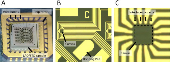
Figure 2. Images of lithographically patterned LAO/STO heterostructures. (A) Image showing 5mm x 5mm sample wire bonded to a chip carrier. (B) Optical image showing bonding pads and one of the canvases. (C) Close-up of a single canvas. Please click here to view a larger version of this figure.

Figure 3. (A) Informal design of LAO/STO nanostructure. (B) Precise layout of nanostructure using an open-source scalable vector graphics (SVG) editor.

Figure 4. (A) Lithography front panel for c-AFM patterning. (B) Screenshot from 3D simulator showing position and voltage of c-AFM tip. Please click here to view a larger version of this figure.

Figure 5. (A) LAO/STO nanostructure being inserted into dilution refrigerator. (B) Monitoring of sample resistance as it is cooled from 300 K to 50 mK. (C) Monitoring of four-terminal differential conductance of device as a function of side gate voltage Vsg and voltage across the device (V4t). Intensity graph displayed in units of siemens (S), and voltages are displayed in units of volts (V).
Discussion
Successful creation of nanostructures depends on several critical steps. It is important that the LAO/STO samples are grown with a thickness that is known to be at the boundary between the insulating and conductive phase. (Details of sample growth fall outside the scope of this paper, but are crucial for overall success.) Second, it is important to have relative humidity within the range 25-45% for successful c-AFM writing. Values below 25% are unlikely to produce conductive nanostructures, while too high humidity will generally produce uncontrollably large features. Also, temperature control of the AFM is important if the c-AFM tip needs to achieve precise registry over long periods of time. Once the nanostructures are created, they must be placed in a vacuum environment if experiments lasting longer than a few hours are to be performed. For the experiments described here, the structure is created and within minutes transferred to a vacuum environment.
It is recommend before writing that a “writing test” be performed on all relevant electrodes. In such a test, two virtual electrodes are first created, and a single nanowire is written while simultaneously monitoring the conductance. A similar test of erasure can be performed by “cutting” the nanowire shortly afterwards. If the nanostructure is decaying rapidly, the issue is most likely due either to the interfacial contacts or the canvas itself. To distinguish between these two effects, a four-terminal measurement of the conductance should be performed, and the two-terminal conductance should be compared with the four-terminal conductance as a function of time. If the two-terminal conductance is decaying more rapidly than the four-terminal conductance, then the issue is related to the electrical contacts to the interface. If the four-terminal conductance is decaying at a comparable rate, then most likely the canvas is not suitable and should be replaced.
There are natural limitations of the current method for creating nanostructures. Specifically, the writing speed for the smallest devices is limited to a few hundred nanometers per second. Speeds far above that value lead to unpredictable results. Use of parallel writing techniques are possible27,28, but are not highly developed and have their own drawbacks. The size of nanostructures that can be created is naturally limited by the scan range of the AFM being used. A high-quality AFM with closed-loop feedback in the two scan directions is highly recommended. Tracking of point-like objects on the sample surface should be performed to monitor temporal drift of the sample.
Once creation of conductive nanostructures at oxide interfaces has been mastered, there are a wide range of experimental directions that can be explored. Using this technique, a wide variety of nanostructures and devices have already been demonstrated, including nanowires18, tunnel barriers29, rectifying junctions30, field-effect transistors18, single-electron transistors31, superconducting nanowires32, nanoscale optical detectors33, and nanoscale THz emitters and detectors34.
Disclosures
The authors have nothing to disclose.
Acknowledgements
The long-standing collaboration with Chang-Beom Eom at the University of Wisconsin-Madison, who provided the LAO/STO samples, is gratefully acknowledged. Video editing assistance from Christopher Solis is greatly appreciated. This work is supported by NSF (DMR-1104191, DMR-1124131), ARO (W911NF-08-1-0317), and AFOSR (FA9550-10-1-0524, FA9550-12-1-0268, FA9550-12-1-0057).
Materials
| Name | Company | Catalog Number | Comments |
|---|---|---|---|
| Equipment | |||
| Contact Aligner | Karl-Suss | MA6 | |
| Spinner | Solitec | 5110C | |
| Ion Mill | Commonwealth Scientific | 8C | |
| Sputtering System | Leybold-Heraeus | Z-650 | |
| Barrel Etcher | Branson/IPC | 3000C | |
| Wire Bonder | Westbond | 7700E | |
| AFM | Asylum Research | MFP-3D | |
| Dilution Refrigerator | Quantum Design | P850 | |
| Ultrasonic Wash Machine | Fisher Scientific | 15-335-6 | |
| Current Amplifier | Femto | DLPCA-200 | |
| Materials | |||
| LaAlO3/SrTiO3 | Prof. Chang-Beom Eom | 5 mm x 1 mm with ~3.4 unit cells of LAO (See Reference 18) | |
| Photoresist | AZ Electronic Materials | P4210 | |
| Developer | AZ Electronic Materials | 400K | |
| Acetone | Fisher Scientific | A929SK-4 | |
| Isopropyl Alcohol | Fisher Scientific | A459-1 | |
| Deionized Water | Fisher Scientific | 23-290-065 | |
| Gold Wire | DuPont | 5771 | 1 mm diameter |
| Chip Carrier | NTK Technologies | IRK28F1-5451D |
References
- Sulpizio, J. A., Ilani, S., Irvin, P., Levy, J. i Annual Review of Materials Research, in press. , (2014).
- Mannhart, J., Blank, D. H. A., Hwang, H. Y., Millis, A. J., Triscone, J. M. Two-Dimensional Electron Gases at Oxide Interfaces. Mrs Bulletin. 33, 1027-1034 (2008).
- Langer, J. S. Annual Review of Condensed Matter Physics. Interface Physics in Complex Oxide Heterostructures. , 141-165 (2011).
- Bogorin, D. F., Irvin, P., Cen, C., Levy, J. i Multifunctional Oxide Heterostructures. Tsymbal, E. Y., Dagotto, E. R. A., Chang-Beom, E., Ramesh, R. 13, University Press. Oxford. (2012).
- Granozio, F. M., Koster, G., Rijnders, G. Functional Oxide Interfaces. MRS Bulletin. 38, 1017-1023 (2013).
- Ohtomo, A., Hwang, H. Y. A high-mobility electron gas at the LaAlO3/SrTiO3 heterointerface. Nature. 427, 423-426 (2004).
- Reyren, N., et al. Superconducting interfaces between insulating oxides. Science. 317, 1196-1199 (2007).
- Bark, C. W., et al. Switchable Induced Polarization in LaAlO3/SrTiO3 Heterostructures. Nano Letters. 12, 1765-1771 (2012).
- Brinkman, A., et al. Magnetic effects at the interface between non-magnetic oxides. Nature Materials. 6, 493-496 (2007).
- Thiel, S., Hammerl, G., Schmehl, A., Schneider, C. W., Mannhart, J. Tunable quasi-two-dimensional electron gases in oxide heterostructures. Science. 313, 1942-1945 (2006).
- Cen, C., et al. Nanoscale control of an interfacial metal-insulator transition at room temperature. Nature Materials. 7, 298-302 (2008).
- Singh-Bhalla, G., et al. Built-in and induced polarization across LaAlO3/SrTiO3 heterojunctions. Nature Physics. 7, 80-86 (2011).
- Li, L., et al. Very Large Capacitance Enhancement in a Two-Dimensional Electron System. Science. 332, 825-828 (2011).
- Xie, Y., Hikita, Y., Bell, C., Hwang, H. Y. Control of electronic conduction at an oxide heterointerface using surface polar adsorbates. Nature Communications. 2, 494(2011).
- Bark, C. W., et al. Tailoring a two-dimensional electron gas at the LaAlO3/SrTiO3 (001) interface by epitaxial strain. PNAS. 108, 4720-4724 (2011).
- Tra, V. T., et al. Adv Mater. 25, 3357-3364 (2013).
- Cronenwett, S. M., Oosterkamp, T. H., Kouwenhoven, L. P. A Tunable Kondo Effect in Quantum Dots. Science. 281, 540-544 (1998).
- Cen, C., Thiel, S., Mannhart, J., Levy, J. Oxide Nanoelectronics on Demand. Science. 323, 1026-1030 (2009).
- Kalinin, S. V., Gruverman, A. Scanning probe microscopy: electrical and electromechanical phenomena at the nanoscale. 1, Springer. (2007).
- Piner, R. D., Zhu, J., Xu, F., Hong, S. H., Mirkin, C. A. 'Dip-pen' nanolithography. Science. 283, 661-663 (1999).
- Ahn, C. H., et al. Nonvolatile Electronic Writing of Epitaxial Pb(Zr0.52Ti0.48)O3/SrRuO3 Heterostructures. Science. 276, 1100-1103 (1997).
- Bi, F., et al. 'Water-cycle' mechanism for writing and erasing nanostructures at the LaAlO3/SrTiO3 interface. Applied Physics Letters. 97, 173110(2010).
- Cheng, G., et al. Anomalous Transport in Sketched Nanostructures at the LaAlO3/SrTiO3 Interface. Phys Rev X. 3, 011021(2013).
- Veazey, J. P., et al. Nonlocal current-voltage characteristics of gated superconducting sketched oxide nanostructures. Europhys Lett. 103, 57001(2013).
- Veazey, J. P., et al. Oxide-based platform for reconfigurable superconducting nanoelectronics. Nanotechnology. 24, 375201(2013).
- Irvin, P., et al. Anomalous High Mobility in LaAlO3/SrTiO3 Nanowires. Nano Letters. 13, 364-368 (2013).
- Salaita, K., et al. Massively Parallel Dip–Pen Nanolithography with 55 Two-Dimensional Arrays. Angewandte Chemie. 118, 7378-7381 (2006).
- Li, S., et al. Parallel Conductive-AFM Lithography on LaAlO3/SrTiO3 Interfaces. Ieee T Nanotechnol. 12, 518-520 (2013).
- Cen, C., Bogorin, D. F., Levy, J. Thermal activation and quantum field emission in a sketch-based oxide nanotransistor. Nanotechnology. 21, 475201(2010).
- Bogorin, D. F., et al. Nanoscale rectification at the LaAlO3/SrTiO3 interface. Applied Physics Letters. 97, 013102(2010).
- Cheng, G., et al. Sketched Oxide Single-Electron Transistor. Nature Nanotech. 6, 343-347 (2011).
- Joshua, A., Ruhman, J., Pecker, S., Altman, E., Ilani, S. Gate-tunable polarized phase of two-dimensional electrons at the LaAlO3/SrTiO3 interface. PNAS. 110, 9633(2013).
- Irvin, P., et al. Rewritable Nanoscale Oxide Photodetector. Nature Photon. 4, 849-852 (2010).
- Ma, Y., et al. Broadband Terahertz Generation and Detection at 10 nm Scale. Nano Letters. 13, 2884-2888 (2013).
Reprints and Permissions
