

Summary
This article describes the growth of epitaxial films of Mg3N2 and Zn3N2 on MgO substrates by plasma-assisted molecular beam epitaxy with N2 gas as the nitrogen source and optical growth monitoring.
Abstract
This article describes a procedure for growing Mg3N2 and Zn3N2 films by plasma-assisted molecular beam epitaxy (MBE). The films are grown on 100 oriented MgO substrates with N2 gas as the nitrogen source. The method for preparing the substrates and the MBE growth process are described. The orientation and crystalline order of the substrate and film surface are monitored by the reflection high energy electron diffraction (RHEED) before and during growth. The specular reflectivity of the sample surface is measured during growth with an Ar-ion laser with a wavelength of 488 nm. By fitting the time dependence of the reflectivity to a mathematical model, the refractive index, optical extinction coefficient, and growth rate of the film are determined. The metal fluxes are measured independently as a function of the effusion cell temperatures using a quartz crystal monitor. Typical growth rates are 0.028 nm/s at growth temperatures of 150 °C and 330 °C for Mg3N2 and Zn3N2 films, respectively.
Introduction
The II3-V2 materials are a class of semiconductors that have received relatively little attention from the semiconductor research community compared to III-V and II-VI semiconductors1. The Mg and Zn nitrides, Mg3N2 and Zn3N2, are attractive for consumer applications because they are composed of abundant and non-toxic elements, making them inexpensive and easy to recycle unlike most III-V and II-VI compound semiconductors. They display an anti-bixbyite crystal structure similar to the CaF2 structure, with one of the interpenetrating fcc F-sublattices being half-occupied2,3,4,5. They are both direct band gap materials6, making them suitable for optical applications7,8,9. The band gap of Mg3N2 is in the visible spectrum (2.5 eV)10, and the band gap of Zn3N2 is in the near-infrared (1.25 eV)11. To explore the physical properties of these materials and their potential for electronic and optical device applications, it is critical to obtain high quality, single crystal films. Most work on these materials to date has been carried out on powders or polycrystalline films made by reactive sputtering12,13,14,15,16,17.
Molecular beam epitaxy (MBE) is a well-developed and versatile method for growing single-crystal compound semiconductor films18 that has the potential to yield high quality materials using a clean environment and high-purity elemental sources. Meanwhile, MBE rapid shutter action enables changes to a film at the atomic layer scale and allows for precise thickness control. This paper reports on the growth of Mg3N2 and Zn3N2 epitaxial films on MgO substrates by plasma-assisted MBE, using high purity Zn and Mg as vapor sources and N2 gas as the nitrogen source.
Subscription Required. Please recommend JoVE to your librarian.
Protocol
1. MgO substrate preparation
NOTE: Commercial one-side epi-polished (100) oriented single crystal MgO square substrates (1 cm x 1 cm) were employed for the X3N2 (X = Zn and Mg) thin film growth.
- High temperature annealing
- Place the MgO on a clean sapphire wafer sample carrier with the polished side facing upwards in a furnace and anneal for 9 h at 1,000 °C. Raise the temperature to 1000 °C over a 10 min period.
NOTE: High temperature annealing removes carbon from the surface and reconstructs the surface crystal structure of the MgO single crystal substrates. - Cool the MgO substrates to the room temperature (RT).
- Place the MgO on a clean sapphire wafer sample carrier with the polished side facing upwards in a furnace and anneal for 9 h at 1,000 °C. Raise the temperature to 1000 °C over a 10 min period.
- Substrate cleaning
- Collect the annealed MgO substrates and rinse in deionized water in a clean borosilicate glass beaker.
- Boil the MgO substrates in 100 mL of acetone in a 250 mL borosilicate glass beaker for 30 min to remove inorganic carbon contamination from handling.
NOTE: Cover the beaker and do not allow the acetone to boil dry. - Drain the acetone and rinse the MgO substrates in 50 mL of methanol.
- Blow-dry the substrates with nitrogen gas, then store the dry, clean substrates in the clean chip tray.
2. Operation of VG V80 MBE
- Open the cooling water for the preparation chamber, cryoshroud on the growth chamber (see Figure 1), effusion cells, and quartz crystal microbalance sensor.
- Turn on the Ar-ion laser with a wavelength of 488 nm. The laser light is brought to the MBE chamber with an optical fiber from the laser, which is located in another room.
- Turn on the reflection high energy electron diffraction gun (RHEED), 13.56 Mhz radio frequency (rf) plasma generator, and quartz crystal microbalance (QCM) system.
3. Substrate loading
- Fast entry lock
- Mount a clean MgO substrate on the molybdenum sample holder (Figure 2A) using tungsten spring clips.
- Turn off the turbo pump on the fast entry lock (FEL) and vent the FEL chamber with nitrogen. Open the FEL when the chamber pressure reaches atmospheric pressure.
- Remove the sampler holder cassette out of the FEL and load the sample holder with the substrate into the cassette.
- Load the cassette back into the FEL and turn the turbo pump back on.
- Wait for the pressure in the FEL to drop to 10-6 Torr.
- Increase the temperature of the fast entry lock to 100 °C over a period of 5 min and degas the substrates with the holders for 30 min in the fast entry lock.
- Make sure the pressure in the fast entry lock is below 10-7 Torr before opening the vacuum valve to the preparation chamber. Transfer the holder using the wobble stick transfer mechanism to the preparation chamber, then ramp up the degassing station to 400 °C and allow it to degas for 5 h.
- Transfer the degassed holder by the trolley transfer mechanism to the sample manipulator in the growth chamber. Increase the substrate temperature up to 750 °C over a period of 30 min and allow the sample to outgas in the manipulator for another 30 min. Make sure the cooling water is turned on in the cryoshroud to avoid overheating the cryoshroud.
- Drop the temperature of the substrate to 150 °C for Zn3N2 film growth and 330°C for Mg3N2 film growth using the thermocouple in the sample manipulator to measure the sample temperature.
- In-situ RHEED
- Set the voltage on the electron gun to 15 kV and filament current to 1.5 A once the growth chamber pressure is below 1 x 10⁻⁷ Torr.
- Rotate the substrate holder until 1) the electron gun is aligned along a principle crystallographic axis of the substrate and 2) a clear single crystal electron diffraction pattern is visible.
- Take a picture of the RHEED pattern and save the picture.
- Close the shutter on the effusion cell and stop the flow of nitrogen. Measure the RHEED pattern for the deposited film when the chamber pressure is below 10-7 Torr.
4. Metal flux measurements
- Use standard group III type effusion cells or low temperature effusion cells for Mg and Zn.
- Load the crucibles with 15 g and 25 g of high purity Mg and Zn shot, respectively.
- When the growth chamber has achieved a vacuum of 10-8 Torr or better, and before loading the substrate holder, outgas the Zn or Mg source effusion cells up to 250 °C at a ramp rate of ~20 °C/min and allow it to outgas for 1 h with the shutters closed.
- After the substrate has been loaded into the sample manipulator, heat the Zn and/or Mg effusion cells to 350 °C or 390 °C respectively, at a ramp rate of ~10 °C/min, and wait 10 min for them to stabilize with the shutters closed.
- Use the retractable quartz crystal monitor to measure the metal flux. Position the quartz crystal sensor in front of the substrate inside the chamber. Make sure the substrate is fully covered by the detector so that no metal is deposited on the substrate.
- Input the density of the metal of interest (ρZn = 7.14 g/cm3, ρMg = 1.74 g/cm3) into the quartz crystal monitor (QCM) controller.
- To calibrate the flux, open the shutter for one of the metal sources and allow the effusion cell to deposit on the sensor. The QCM system converts its internal measurement of mass to thickness.
- Calculate the elemental flux from the slope of the increasing thickness as a function of time shown on the QCM. The rate of increase of the thickness over a few minutes is proportional to the elemental flux. In two example cases, a Zn flux of 0.45 nm/s and a Mg flux of 1.0 nm/s are obtained.
- Change the temperature of the effusion cells and repeat step 4.8 if the temperature dependence of the flux is required. The measured temperature dependence of the Mg and Zn flux is shown in Figure 3 for this specific growth system.
- When the flux measurements are complete, close the shutters on the effusion cells and retract the quartz crystal sensor.
5. Nitrogen plasma
- Turn off the filament current and high voltage on the RHEED gun to prevent damage in the presence of a high N2 gas pressure in the growth chamber.
- Open the gas valve on the high pressure N2 cylinder.
- Slowly open the leak valve slowly until the nitrogen pressure in the growth chamber reaches 3 x 10⁻⁵-4 x 10⁻⁵ Torr.
- Set the power of the plasma generator to 300 W.
- Ignite the plasma with the ignitor on the plasma source. A bright purple glow will be visible from the viewport when the plasma ignites, as shown in Figure 2B.
- Adjust the control on the rf matching box to minimize the reflected power as much as possible. A reflected power of less than 15 W is good; in this case, the reflected power is reduced to 12 W.
6. In situ laser light scattering
- Focus the chopped 488 nm Argon laser light reflected from the substrate in the growth chamber onto the Si photodiode so that an electrical signal can be detected by the lock-in amplifier. This is accomplished by adjusting the angle of the substrate by rotating the substrate holder around two axes and adjusting the position of the Si detector, then focusing the lens that collects the reflected light as shown in Figure 4.
- Open the shutter of one of the metal sources.
- Record the time-dependent reflectivity with a computer-controlled data logger. The growth of an epitaxial film will produce an oscillatory reflected signal with time associated with thin film optical interference between the front and back surfaces of the film.
- To protect the film from oxidation in air, deposit an encapsulation layer to protect the film from oxidation in air. This is especially important for Mg3N2 which oxidizes rapidly in air.
- In order to deposit a MgO encapsulation layer, close the nitrogen gas, switch to oxygen gas, repeat step 5.3, and increase the oxygen pressure to 1 x 10⁻⁵ Torr.
- Set the power of the plasma generator to 250 W and repeat step 5.5. The plasma starts at lower rf power with oxygen gas than with nitrogen gas.
- Open the shutter on the Mg source, and repeat step 6.4 for 5-10 min.
NOTE: This will produce a MgO film that is about 10 nm thick. The uncapped Mg3N2 films are yellow but fade quickly to a whitish color within 20 s upon exposure to air. Consequently, an encapsulation layer is required to allow time for measurements on the films before they oxidize after removal from the vacuum chamber. - Close the gas valves, turn off the laser, and ramp down the substrate and cell temperatures to ~25 °C in 30 min. Turn off the cooling water and the rf power to the plasma source.
- After several growth runs, the optical windows become covered with metal. Remove the metal by wrapping the window in aluminum foil and heating it with heating tape to 400 °C and a temperature ramp rate of ~15 °C/min or slower over the course of a weekend.
7. Growth rate determination
- Use Equation 1 below to describe the optical reflectivity of the sample11,19.
 (1)
(1)
Where:
 (1 - a)
 (1 - b)
 (1 - c)
 (1 - d)
 - And where: n2 = 1.747 is the refractive index of the MgO substrate at a wavelength of 488 nm; θ0 is the angle of the incident beam measured with respect to the substrate surface normal; and t is time. The optical constants of the film (n1 and k1) and growth rate are obtained by fitting the reflectivity as a function of time in Equation 1.
 (1)
(1) (1 - a)
 (1 - b)
 (1 - c)
 (1 - d)
Subscription Required. Please recommend JoVE to your librarian.
Representative Results
The black object in the inset in Figure 5B is a photograph of an as-grown 200 nm Zn3N2 thin film. Similarly, the yellow object in the inset in Figure 5C is an as-grown 220 nm Mg3N2 thin film. The yellow film is transparent to the extent that it is easy-to-read text placed behind the film10.
The surface of the substrate and the films were monitored in situ by RHEED. Figure 5A shows the RHEED pattern of a bare substrate with the electron beam incident along the [110] direction of the substrate. RHEED patterns for the deposited films in Figure 5B,C show that the crystal lattices of the Zn3N2 and Mg3N2 thin films are oriented in the plane of the substrate surface, as expected in the case of epitaxial growth. The disadvantage of RHEED for growth monitoring under the conditions used here is that the growth process must be stopped to allow the pressure to drop to 10-7 Torr and turn on the electron gun.
In contrast with RHEED, in situ optical reflectivity measurements are not affected by pressure in the chamber. To obtain the growth rate, in situ optical reflectivity was fit as a function of time shown in Figure 6 using Equation 1. In this equation, growth time t is the independent variable, and the optical constants of the film (n1, k1) and growth rate are fitting parameters. In Figure 6, the MgO substrate refractive index, angle of incidence, and wavelength are n2 = 1.747, θ0 = 36.5°, and λ = 488 nm, respectively. The fitted refractive index of the film is n1 = 2.65, extinction coefficient is k1 = 0.54, and growth rate is = 0.031 nm/s for the Zn3N2 thin film as shown in Figure 6A. Similarly, the best fit refractive index for the Mg3N2 film is n1 = 2.4, extinction coefficient is k1 = 0.09, and growth rate is = 0.033 nm/s as shown in Figure 6B. The overall decrease in the specular reflection with time in Figure 6B is believed to be caused by an increase in surface roughness scattering as the Mg3N2 thin film becomes thicker. The effect of the roughness scattering was simulated by multiplying the calculated reflectivity with a decaying exponential, e-βt, where β = 810-5 s-1 and the growth time t ismeasured in seconds.
Upon exposure to air, the uncapped yellow Mg3N2 films faded within minutes to a translucent white color. On the other hand, the Mg3N2 films that were capped with MgO were relatively stable. To further protect the capped Mg3N2 films from oxidation, the Mg3N2/MgO heterostructures were coated with a CaF2 layer deposited by electron beam evaporation. Uncapped Zn3N2 is more stable; however, the initially black Zn3N2 films also oxidized over time and turned grey within a few months. The oxidation reaction is believed to involve the formation of magnesium hydroxide and release ammonia according to the following chemical reaction20. A ZnO layer deposited using a similar method to the MgO can also be used as a protective layer to prevent oxidation.
Mg3N2 + 6H2O → 3Mg(OH)2 + 2NH3

Figure 1: View of the VG V80H molecular beam epitaxy growth chamber. This picture shows the MBE growth chamber with (clockwise) the RHEED screen and camera housing, quadrupole residual gas analyzer, optical hardware on laser light scattering port, Mg effusion cell, N-plasma source, rf matching box, and the Zn effusion cell. Please click here to view a larger version of this figure.

Figure 2: Substrate holder and glow from plasma source. (A) Molybdenum sample holder plate with two tungsten wire clips holding the square MgO substrate in place. (B) Purple glow originating from the back window of the plasma source when operating with N2 gas. Please click here to view a larger version of this figure.
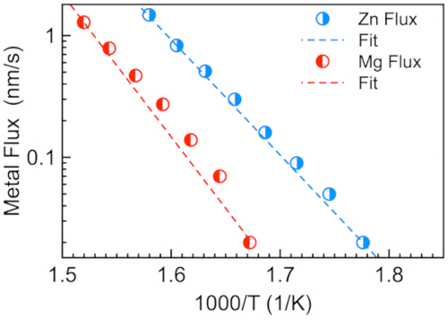
Figure 3: Metal flux as a function of effusion cell temperature. The lines are fit to the temperature dependence of the metal fluxes using an Arrhenius relation as discussed in the text. Please click here to view a larger version of this figure.

Figure 4: Schematic of the in-situ laser light scattering setup. Please click here to view a larger version of this figure.

Figure 5: RHEED patterns. (A) RHEED diffraction pattern for MgO substrate. (B) RHEED pattern of as-grown Zn3N2 film with photograph of black Zn3N2 film. (C) RHEED pattern of as-grown Mg3N2 substrate with photograph of yellow Mg3N2 film. Please click here to view a larger version of this figure.

Figure 6: In situ specular reflectivity. In situ specular reflectivity at 488 nm of (A) Zn3N2 and (B) Mg3N2 films during growth. The calculated reflectivity (red line) is best-fit to the experimental data (blue circles) as discussed in the text. Please click here to view a larger version of this figure.
Subscription Required. Please recommend JoVE to your librarian.
Discussion
A variety of considerations is involved in the choice of substrates and establishing the growth conditions that optimize the structural and electronic properties of the films. The MgO substrates are heated at high temperature in air (1000 °C) to remove carbon contamination from the surface and improve the crystalline order in the substrate surface. Ultrasonic cleaning in acetone is a good alternative method to clean the MgO substrates.
The (400) X-ray diffraction peak for the Zn3N2 films was found to be narrower when the film was grown on high-temperature, annealed MgO substrates compared to when grown on unannealed substrates. The lattice constant of MgO (0.421 nm) is significantly smaller than (half of) the lattice constant of Zn3N2 (0.976 nm) or Mg3N2 (0.995 nm) and not well-matched to the semiconductor films. The lattice constants of the commercially available groups IV, III-V, and II-VI substrates are all larger than the lattice constants of Mg3N2 and Zn3N2. A more well-matched substrate is desirable. Silicon, which has a lattice constant of 0.543 nm, is somewhat more well-matched to Mg3N2 than MgO and is worth to be explored. Zn3N2 films were also grown on A-plane sapphire substrates. The structural quality of these films was not as good as that seen in the MgO substrates, as indicated by the RHEED spots and width of the (400) Zn3N2 X-ray diffraction peak. In the case of the sapphire substrates, the backside was coated with Cr (50 nm) and Mo (200 nm) to improve thermal coupling between the substrate holder and substrate.
The substrate temperature is measured during growth with a thermocouple located in the enclosed vacuum space between the substrate holder and heater, and it is not in physical contact with the substrate holder or the substrate. As a result, it was expected that the actual substrate temperature would be lower than the sensor temperature. Successful Mg3N2 and Zn3N2 growths were obtained with thermocouple temperatures in the 300-350 °C and 140-180 °C ranges, respectively.
High growth temperature increases the mobility of the ad-atoms on the growing surface and may be expected to produce material with fewer structural defects. However, at high substrate temperatures, the growth rate is lower, which is interpreted as being due to re-evaporation of metal atoms from the surface. At high metal flux, film growth rate is limited by the supply of active nitrogen. The active nitrogen is maximized at high rf power applied to the plasma source (300 W max) and at a high nitrogen flow rate. The N2 flow rate is limited by the maximum pressure in the growth chamber, which in this case was in the mid 10-5 Torr range. Ammonia is a possible alternative nitrogen source. Mg and Zn will react with NH3 at a high temperature without plasma activation; however, it is unclear whether the residence time of Mg and Zn atoms on the surface will be long enough to support film growth at temperatures for which NH3 will react with the metals.
In these experiments, effusion cells were used with pyrolytic boron nitride (PBN) crucibles with capacities of 40 cc for Mg and 25 cc for Zn. Figure 3 shows the temperature dependence of the Mg and Zn fluxes from the effusion cells. The straight lines in Figure 3 are fit to the measured temperature dependence of the fluxes. The fits have the form Flux = A exp(-B/kT), and the fitting parameters (A,B) are (8.5 x 10¹⁷ nm/s, 2.3 eV) and (1.3 x 10¹⁵ nm/s, 1.9 eV) for the Mg and Zn sources, respectively. The flux approximately doubles with each 10 °C and 12 °C increase in the effusion cell temperature for Mg and Zn, respectively. For the growth illustrated in Figure 6, the metal fluxes were near the maxima in Figure 3 (~1 nm/s with Mg flux higher than Zn flux) but the film growth rates were only 0.03 nm/s. This shows that the metal utilization efficiency is low, with Mg being lower than Zn and most of the metal re-evaporating.
The high N2 background pressure during growth precludes the continuous monitoring of the film growth with RHEED. Differential pumping of the RHEED gun can solve this problem. In situ optical reflectivity measurements serve as a complementary monitoring tool that is not affected by gas pressure and provides an accurate and reliable technique for determining the growth rate. The non-specular or diffuse reflectivity of the substrate can also be measured in situ and will provide information on surface roughness during growth.
The base pressure in the MBE growth chamber is 10-8 Torr with the N2 gas turned off. The cryoshroud in the growth chamber is cooled with water during film growth. Under these conditions, some residual oxygen contamination can be expected in the films. The residual water vapour pressure in the growth chamber can be reduced with a lower temperature coolant in the shroud, such as silicone oil at -80 °C21.
In conclusion, this protocol describes how to grow single crystal films of Mg3N2 and Zn3N2 by plasma-assisted molecular beam epitaxy and provides suggestions for how the growth process can be changed to further improve film quality. These materials did not show photoluminescence at either room temperature or a low temperature. There is a need to further reduce the defect density in the films. Mg3N2-Zn3N2 alloys can also be grown by plasma-assisted molecular beam epitaxy.
Subscription Required. Please recommend JoVE to your librarian.
Disclosures
The authors have nothing to disclose.
Acknowledgments
This work was supported by the Natural Sciences and Engineering Research Council of Canada.
Materials
| Name | Company | Catalog Number | Comments |
| (100) MgO | University Wafer | 214018 | one side epi-polished |
| Acetone | Fisher Chemical | 170239 | 99.8% |
| Argon laser | Lexel Laser | 00-137-124 | 488 nm visible wavelength, 350 mW output power |
| Chopper | Stanford Research system | SR540 | Max. Frequency: 3.7 kHz |
| Lock-in amplifier | Stanford Research system | 37909 | DSP SR810, Max. Frequency: 100 kHz |
| Magnesium | UMC | MG6P5 | 99.9999% |
| MBE system | VG Semicon | V80H0016-2 SHT 1 | V80H-10 |
| Methanol | Alfa Aesar | L30U027 | Semi-grade 99.9% |
| Nitrogen | Praxair | 402219501 | 99.998% |
| Oxygen | Linde Gas | 200-14-00067 | > 99.9999% |
| Plasma source | SVT Associates | SVTA-RF-4.5PBN | PBN, 0.11" Aperture, Specify Length: 12" – 20" |
| Si photodiode | Newport | 2718 | 818-UV Enhanced, 200 - 1100 nm |
| Zinc | Alfa Aesar | 7440-66-6 | 99.9999% |
References
- Suda, T., Kakishita, K. Band-gap energy and electron effective mass of polycrystalline Zn3N2. Journal of Applied Physics. 99 (7), 076101.1-076101.3 (2006).
- Hu, J., Bando, Y., Zhan, J., Zhi, C., Golberg, D. Carbon nanotubes as nanoreactors for fabrication of single-crystalline Mg3N2 nanowires. Nano Letters. 6 (6), 1136-1140 (2006).
- Fang, C. M., Groot, R. A., Bruls, R. J., Hintzen, H. T., With, G. Ab initio band structure calculations of Mg3N2 and MgSiN2. Journal of Physics: Condensed Matter. 11 (25), 4833-4842 (1999).
- Yoo, S. H., Walsh, A., Scanlonc, D. O., Soon, A. Electronic structure and band alignment of zinc nitride, Zn3N2. RSC Advances. 4 (7), 3306-3311 (2014).
- Partin, D. E., Williams, D. J., O'Keeffe, M. The crystal structures of Mg3N2 and Zn3N2. Journal of Solid-State Chemistry. 132 (1), 56-59 (1997).
- Ullah, M., Murtaza, G., Ramay, S. M., Mahmood, A. Structural, electronic, optical and thermoelectric properties of Mg3X2 (X = N, P, As, Sb, Bi) compounds. Materials Research Bulletin. 91, 22-30 (2017).
- Li, C. T. Electrocatalytic zinc composites as the efficient counter electrodes of dye-sensitized solar cells: study on the electrochemical performance and density functional theory Calculations. ACS Applied Materials & Interfaces. 7 (51), 28254-28263 (2015).
- Sinha, S., Choudhury, D., Rajaraman, G., Sarkar, S. Atomic layer deposition of Zn3N2 thin films: growth mechanism and application in thin film transistor. RSC Advances. 5 (29), 22712-22717 (2015).
- Bhattacharyya, S. R., Ayouchi, R., Pinnisch, M., Schwarz, R. Transfer characteristic of zinc nitride based thin film transistors. Physica Status Solidi C. 9 (3-4), 469-472 (2012).
- Wu, P., Tiedje, T. Molecular beam epitaxy growth and optical properties of Mg3N2 films. Applied Physics Letters. 113 (8), 082101.1-082101.4 (2018).
- Wu, P., et al. Molecular beam epitaxy growth and optical properties of single crystal Zn3N2 films. Semiconductor Science and Technology. 31 (10), 10LT01.1-10LT01.4 (2016).
- Jiang, N., Georgiev, D. G., Jayatissa, A. H. The effects of the pressure and the oxygen content of the sputtering gas on the structure and the properties of zinc oxy-nitride thin films deposited by reactive sputtering of zinc. Semiconductor Science and Technology. 28 (2), 025009 (2013).
- Nakano, Y., Morikawa, T., Ohwaki, T., Taga, Y. Electrical characterization of p-type N-doped ZnO films prepared by thermal oxidation of sputtered Zn3N2 films. Applied Physics Letters. 88 (17), 172103.1-172103.3 (2006).
- Cao, X., Yamaguchi, Y., Ninomiya, Y., Yamada, N. Comparative study of electron transport mechanisms in epitaxial and polycrystalline zinc nitride films. Journal of Applied Physics. 119 (2), 025104.1-025104.10 (2016).
- Jia, J., Kamijo, H., Nakamura, S., Shigesato, Y. How the sputtering process influence structural, optical, and electrical properties of Zn3N2 films. MRS Communications. 8 (2), 314-321 (2018).
- Trapalis, A., Hefferman, J., Farrer, I., Sherman, J., Kean, A. Structural, electrical and optical characterization of as-grown and oxidized zinc nitride films. Journal of Applied Physics. 120 (20), 205102.1-205102.9 (2016).
- Núñez, C. G., et al. On the zinc nitride properties and the unintentional incorporation of oxygen. Thin Solid Films. 520 (6), 1924-1929 (2012).
- Oshima, T., Fujita, S. (111)-oriented Zn3N2 growth on a-plane sapphire substrates by molecular beam epitaxy. Japanese Journal of Applied Physics. 45 (111), 8653-8655 (2006).
- Heavens, O. S. Optical properties of thin solid films. , Butterworth, London. 46-48 (1955).
- Heyns, A. H., Prinsloo, L. C., Range, K. J., Stassen, M. The vibrational spectra and decomposition of α-calcium nitride (α-Ca3N2) and magnesium nitride (Mg3N2). Journal of Solid-State Chemistry. 137, 33-41 (1998).
- Lewis, R. B., Bahrami-Yekta, V., Patel, M. J., Tiedje, T., Masnadi-Shirazi, M. Closed-cycle cooling of cryopanels in molecular beam epitaxy. Journal of Vacuum Science Technology B. 32 (2), 02C102.1-02C102.7 (2014).