Here, we fabricate 3D polymeric micro/nano structures in which both the shape and the molecular alignment can be engineered with nanometer scale accuracy by the use of direct laser writing. Light induced deformation of several types of liquid crystalline elastomer microstructures can be controlled in the microscopic scale.
Method Article
Free-form Light Actuators — Fabrication and Control of Actuation in Microscopic Scale
In This Article
Summary
Abstract
Liquid crystalline elastomers (LCEs) are smart materials capable of reversible shape-change in response to external stimuli, and have attracted researchers' attention in many fields. Most of the studies focused on macroscopic LCE structures (films, fibers) and their miniaturization is still in its infancy. Recently developed lithography techniques, e.g., mask exposure and replica molding, only allow for creating 2D structures on LCE thin films. Direct laser writing (DLW) opens access to truly 3D fabrication in the microscopic scale. However, controlling the actuation topology and dynamics at the same length scale remains a challenge.
In this paper we report on a method to control the liquid crystal (LC) molecular alignment in the LCE microstructures of arbitrary three-dimensional shape. This was made possible by a combination of direct laser writing for both the LCE structures as well as for micrograting patterns inducing local LC alignment. Several types of grating patterns were used to introduce different LC alignments, which can be subsequently patterned into the LCE structures. This protocol allows one to obtain LCE microstructures with engineered alignments able to perform multiple opto-mechanical actuation, thus being capable of multiple functionalities. Applications can be foreseen in the fields of tunable photonics, micro-robotics, lab-on-chip technology and others.
Introduction
Microactuators are microscopic structures that can transmit external energy for the operation of another mechanism or system. Due to the compact size and remote control capability, they have been widely used in lab-on-chip systems1, micro-sensing2, and micro robotics3. The actuators available to date can perform only simple actions, such as swelling/collapse in a hydrogel matrix4, contraction/bending5 in one direction with the external field. Although the recently developed techniques have enabled to fabricate microscopic scale actuating structures6, it is still a big challenge to control these actuations in the same length scale. This paper reports a method to prepare 3D light activate microstructures with controllable actuation properties. The technique is based on direct laser writing (DLW), and it is demonstrated in liquid crystalline elastomers (LCEs).
LCEs are soft polymers combing the property of elastomer and liquid crystalline orientation. These materials are capable of large deformation (20 - 400%) under various types of external stimuli7. The advantage of using LCEs for microactuators is the convenience of engineering molecular order in the structures, which allows for controlling the actuation in the microscopic scale8. LC monomers are synthesized with acrylate moiety, enabling a single-step photo-polymerization. This property gives access to different types of lithographic techniques for fabrication of 3D microstructures. Azo-dyes as photo responsive molecules are linked to the polymer network by co-polymerization process. Such molecules combine their strong light response ability (trans to cis isomerization) with the light induced heating of the system affording light controlled deformation.
DLW is a technique to obtain polymer structures in a photosensitive material by spatial control of a focused laser beam9. DLW enables the creation of 3D free-form structures in LCE without losing the molecular alignment6. There are several advantages of DLW in the fabrication of LCE microactuators. First, the resolution can reach the submicron scale, and the structures are truly 3D6. Previously reported LCE micro fabrication methods, e.g., masked exposure10 and replica molding11, provided resolution down to around 10 µm and only have 2D geometry. Secondly, DLW is a non-contact fabrication process. A suitable solvent can develop high quality structures maintaining the designed configuration. Replica molding technique rarely gives sub-micron resolution12 and the structural quality is hard to control. Thirdly, laser writing provides versatile options for local LC orientation at the microscopic scale8,13. Among various types of LC orientation techniques, rubbing is the most efficient way to orientate LC molecules and has been widely used in preparing of LCE thin film. This has been generally achieved by rubbing on polymer layers to generate microgrooves on the inner surfaces of a cell infiltrated by LC monomers. Due to the surface anchoring effect, such microgrooves are able to orientate the LC molecule along the groove direction. DLW enables the direct fabrication of those microgrooves on the selected region in the pre-designed direction with much higher accuracy. All these features make DLW a perfect, unique technique for fabrication and control of actuation in the microscopic scale.
Based on DLW, LCE microstructures may be patterned with different molecular orientations. With compound alignment within a single LCE structure, multifunctional actuations become possible. The method can be used for fabrication of LCE microactuators with any kind of LC monomer mixture. By further chemical engineering, it is possible to make the actuators sensitive to other stimulus sources, e.g., humidity or illumination at different wavelength.
Protocol
Note: This protocol contains three steps: IP-L grating preparation for LC molecular orientation, DLW in the LCE and light actuation characterization. The schematic of direct laser writing system is shown in Figure 1, while the micro-manipulation system is shown in Figure 5.
1. IP-L Grating Pattern Preparation
- Take out one microscope cover slide (3 cm in diameter), and clean it with acetone using lens tissues.
- Place some spacers (glass microspheres) with the help of a metal tip at 3 different points of the glass slide about 0.5 cm away from its center.
- Place another microscope slide (1 cm in diameter) on the top of the spacers. Use a tip to press gently on the top of the upper glass slide.
- Place a drop (around 2 µl) of UV-curing glue on three different points respectively at the boundary of the upper glass.
- Before the glue penetrates too much into the gap, use UV light to solidify the glue. The cell is now formed.
- Place a drop (around 10 µl) of IP-L resin on the boundary of the cell using a pipette. Wait for a few minutes until the liquid is infiltrated into the entire area of the cell.
- Use glue to fix the cell on the sample holder and place it into the direct laser writing system.
- Choose a 100X objective, and find the interface at the upper inner surface, followed by tilt correction on this surface.
- Write the structures of designed IP-L grating patterns with a laser power and a scan speed of 6 mW and 60 µm/sec, respectively. The grating patterns are made by IP-L curve or straight lines.
- Repeat steps 1.8 & 1.9 on the lower inner surface.
- Take out the cell, and immerse the sample in a 2-propanol bath without opening the cell, for 12 - 24 hr.
- Take out the cell from the solvent, and dry it on the hot plate (50 °C) for 10 - 20 min.
2. LCE Microstructure Fabrication
- Measure ~300 mg monomer mixture on the balance. See the molecular composition in Table 1.
- Put the prepared mixture inside a glass bottle, and put it on a hot plate set at 70 - 80 °C.
- Wait until all the powder melts, add a magnetic stirrer, and mix the mixture for 1 hr (90 - 150 rpm).
- Place the cell on the hot plate at 60 °C.
- Place a drop (around 20 µl) of mixture on the edge of the smaller glass slide and wait until the liquid infiltrates into the cell.
- Transfer the cell to the optical microscope with a crossed polarizer and a temperature controller. Keep everything in the dark during transfer, and put an orange filter before the illumination lamp to filter out the UV.
- Increase the temperature of the cell above 60 °C by using a temperature controller on the microscope, then decrease the temperature (2 - 10 °C per min), to measure the temperature range for LC phase. A mixture with different molecular composition has a different LC phase temperature. A good homogeneous nematic LC phase can be recognized by observing the image contrast inversion while rotating the sample every 45° with respect to the polarizer axis.
- Fix the cell on the sample holder, place it into the DLW system, and set the temperature to reach the LC phase (measured in step 2.7).
- Find the interface at the lower inner surface and perform the tilt correction using a 100X objective, or a 10X objective without finding the interface.
- Write the LCE structures by the use of DLW with a laser power and a scan speed of 4 mW and 60 µm/sec on the lower glass slide by using 100X objective. Otherwise, use with a laser power and a scan speed of 14 mW and 60 µm/sec by using 10X objective (LCE structure is fabricated throughout the entire sample thickness).
- Take out the cell, and use a blade to open the cell removing the upper glass slide.
- Immerse the structures in a toluene bath for 5 min.
- Take out the sample, and dry in the air for 10 min.
3. Characterization of Light Actuation of LCE Microstructures
- Place the sample in the optical microscope (20X) and focus a laser beam (CW, 532 nm, 50 - 500 mW) by 10X objective on the structures.
- Observe light induced deformation by the optical microscope CMOS camera (frame rate 25.8 fps).
- Use manual control of the micro-manipulation system (Figure 5) to put the glass tip at a position close to the LCE microstructures.
- Switch on the laser at low power (~20 mW), in order to increase the temperature of the LCE (due to light absorption), and thus soften the structure.
- Use a glass tip to pick up one LCE microstructure, and hold it in the air. This process is needed to avoid the adhesion from glass surface.
- Tune the laser to the high power (>100 mW), and observe the LCE structure deform.
- Record the light induced deformation with the microscope camera.
Results
Figure 1 shows the optical set up for laser writing. The system consists of a 780 nm fiber laser generating 130 fsec pulse at the repetition rate of 100 MHz. The laser beam is reflected into a telescope to adjust the beam profile to the optical microscope objective aperture where it is focused into the sample. On the microscope, a 3D piezo stage is installed with a 300 × 300 × 300 µm3 travelling range for sample translation with a maximum speed of 100 µm/sec at 2 nm resolution. Linearly polarized light from a red lamp illuminates the sample from the top, while the image is collected at the bottom by the same objective and reflected by a beam splitter into a CCD camera. Before the camera, another polarizer is used to obtain cross polarized illumination for enhanced contrast.
Figure 2 shows the scanning electron microscope (SEM) images of the laser written IP-L micrograting patterns (Step 1). The groove spacing is in the range of 400 - 1,200 nm, while the height of the grooves (top-to-valley) is around 700 nm. Grating patterns with different orientations can induce different LC alignments, depending on the desired actuation of the LCE element.
Figure 3 shows the LC monomer orientation induced by the IP-L grating patterns (Step 2.7). First, four kinds of micro-grating pattern with 100 × 100 µm2 size each were fabricated on opposite sides of a glass cell (schematically shown in Figure 3a). Due to the surface anchoring, the infiltrated LC monomers have been oriented along with the grating lines direction, thus exhibiting 45° contrast inversion in the polarized optical microscope (POM) image (Figure 3b).
Figure 4 shows the SEM images of an LCE nano dot/line fabricated on IP-L grating networks with different orientation (Step 2.10). Within the grating network, the LCE structures become more confined, with much higher resistance to the development in toluene. A minimum width of the disconnected LCE has been measured to be ~300 nm, which is consistent with the resolution of DLW without the grating pattern. Another interesting approach for photonic application could be the realization of large scale periodic structure. Figure 4 (c, d) shows 2D LCE periodic structures within a micro-grating network. The alignments are well preserved inside these nanostructures, as shown in the inserted POM images of Figure 4 (c, d). However, light induced deformation could not be obtained in these nanostructures. This is because within the IP-L grating, the nano-LCE elements have been highly confined and adhesion prevents any visible deformation.
The micro manipulation system is based on a home-made reflected microscope and is shown schematically in Figure 5. A 10X objective is fixed on a lens tube placed on a vertically standing optical breadboard. A 730 nm IR LED light source is used for illumination through a non-polarized beam splitter. The reflected image is collected by the same objective and projected on the camera. A continuous solid state 532 nm laser is coupled into the objective by a long pass dichroic mirror (50% transmission and reflection at 567 nm) at an incidence angle of 45°. A power meter measures the transmitted beam after the dichroic mirror for real time detection of laser power. A loosely focused laser spot of ~150 µm diameter generates maximum illumination intensity of ~10 W/mm2. Laser intensity is controlled by a variable neutral density filter placed in front of the laser. Below the objective, a 3D manual translation stage is used for sample translation. A heating stage installed on the translation stage is used for precise control of the sample temperature in a range from -20 to 120 °C with 0.5 °C accuracy. Two glass tips mounted on two manual translation stages have been placed on the left and right sides, near the sample position. Structure micro manipulation can be realized by carefully moving the tips with the help of the translation stages.
To demonstrate the alignment and deformation correlation, we fabricate four LCE cylindrical structures with 60 µm diameter and 20 µm height. These cylinders are written on four differently orientated IP-L grating regions (1 µm period). Under light excitation, the dyes inside the LCE absorb light energy and transfer it into the network. The LCE structures are heated up and then undergo phase transition (nematic to isotropic). Such phase transition is also helped by the trans to cis isomerization of the dye under the same light stimuli. Thus, the structures contract along the original LC alignment director and expand in the perpendicular direction7. Depending on different local alignments induced by the IP-L gratings, these structures deform along different directions, as shown in Figure 6 (Step 3.1).
This technique enables the creation of compound actuators, which contain more than one type of alignment in one single structure. A 400 × 40 × 20 µm3 size LCE stripe with two sections of alignment pattern was fabricated, as schematically shown in Figure 7 (a). Those alignment sections contain each a 90° twisted orientation in a different direction. The surface with parallel alignment contracts, while the one with perpendicular alignment expands under light illumination. The structure has been picked up by the micromanipulation system, and held in the air by a glass tip. Double bending was observed under light illumination (Step 3.3). A modulated laser beam (using an optical chopper) can induce cyclical deformations. LCE can respond following the laser modulation frequency (>1k Hz). However, the deformation amplitude decreases with increasing frequency14.
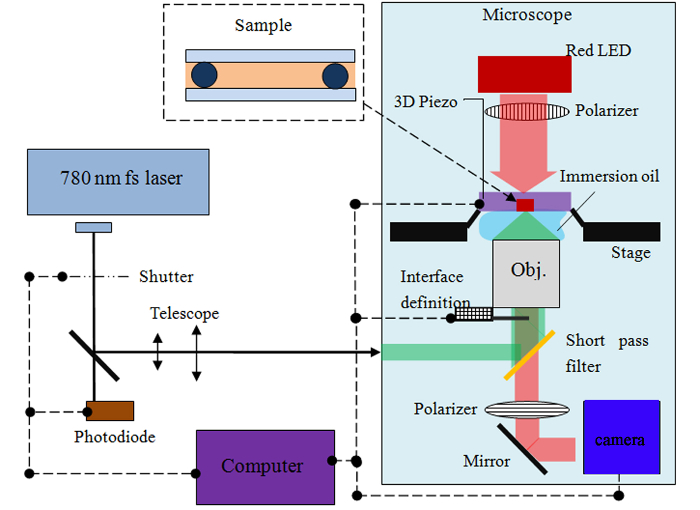
Figure 1: Optical Set Up for Direct Laser Writing. A 780 nm laser beam (130 fsec pulse, repetition rate of 100 MHz) is coupled into a microscope and focused by an optical microscope objective into the sample. A 3D piezo stage with 300 × 300 × 300 µm3 travel range is used for the sample translation during laser exposure. Please click here to view a larger version of this figure.
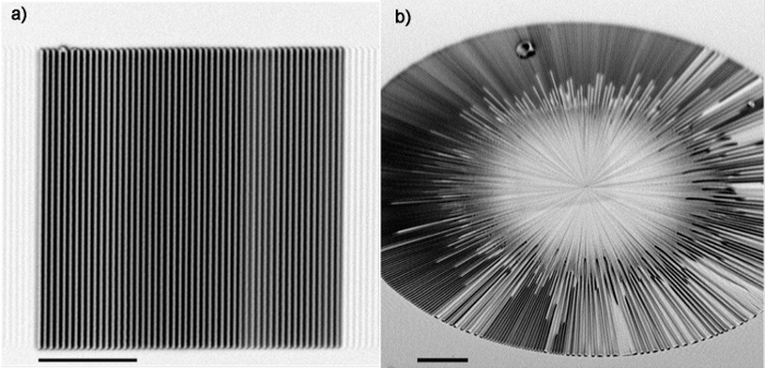
Figure 2: SEM Images of IP-L Micro-gratings. a) Unidirectional parallel line structure. b) Radial grating pattern. Scale bar: 10 µm. Please click here to view a larger version of this figure.
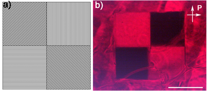
Figure 3: IP-L Micro-grating Induce LC Orientation. a) Schematic of the micro-grating patterns designed for the LC orientation. b) POM image of the the LC orientation induced by the micrograting patterns. The scale bar is 50 µm. The red color is due to the filter which prevents the photo-polymerization. Please click here to view a larger version of this figure.

Figure 4: SEM Images of LCE Nanostructures Embedded Inside IP-L Grating Networks. a) and b) Two micro-grating patterns were fabricated by DLW along different directions, while LCE nanodots are fabricated within the grating network. c) and d) Periodic LCE nano structures embedded within the same type of IP-L gratings. Insets are POM image of the structures. Please click here to view a larger version of this figure.
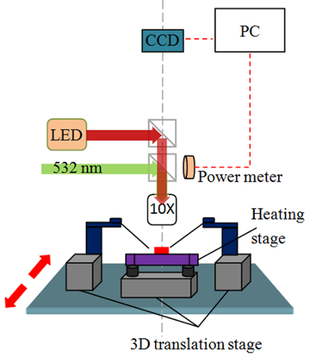
Figure 5: Schematic of the Micromanipulation Setup. A CW solid state 532 nm laser is coupled into a home-made microscope system. A 10X Objective is used for imaging and focusing the 532 nm laser for excitation. Two manual translation stages equipped with glass tip manipulators are used for sample micro-manipulation. Please click here to view a larger version of this figure.
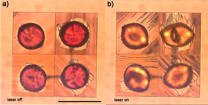
Figure 6: Light Actuation of LCE Micro-cylinders on Four Different IP-L Micrograting Regions with Different Orientations. a) Four LCE cylindrical structures with 60 µm diameter and 20 µm height, written on four differently orientated micro-grating regions. b) LCE cylinders deform along different axes (depending on the grating induced alignments) when exposed to a 532 nm laser radiation (10 W mm-2). Scale bar: 100 µm. Please click here to view a larger version of this figure.
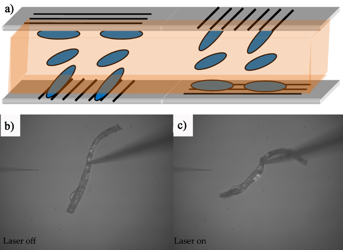
Figure 7: Light-driven Deformation of LCE Microstructures with Multiple Molecular Alignments. a) Schematic of two sections of opposite 90° twisted alignments in a single LCE stripe. b) and c) Optical images of a 400 µm long LCE stripe bending in opposite directions under 532 nm laser illumination (3 W mm-2)8. Please click here to view a larger version of this figure.
Discussion
IP-L micro-grating orientation technique has been integrated with DLW to orientate liquid crystalline monomers. The subsequently laser-written LCE micro-structures can also be patterned with the designed alignment in the micro scale. This technique allows us to create compound LCE elements which can support multiple functionalities. With outstanding ability to create accurate 3D microstructures and control of actuation, we expect this technique to be used for creating elastomer based microscopic robots14, and to open up a plethora of new strategies for the obtainment of light tunable devices15.
There are two critical steps in the preparation. The first one is that the two glasses of the cell should be tightly glued (step 1.4, 1.5). The UV curing glue preserves the stability of the cell geometry during the development: the movement of a glass of the cell in respect to the other will result in a worst alignment of the LCE. Secondly, the laser writing speed during LCE structure writing should be as high as possible while 100X objective is chosen. Due to the strong swelling of the LCE during the laser writing process, the swelled structure would move out the designed position, thus affecting the quality of the fabricated actuators.
In some cases, the light induced deformability is observed to deteriorate in the structures. This could be due to the dye bleaching under high illumination intensity. Once the dye molecules have been switched off, the LCE structure behaves as a transparent medium, and the light absorption/light induced deformation is suppressed. A lower laser power would be safer for the actuation of LCE microstructures.
There are also some disadvantages of this method. Firstly, the whole process takes a relatively long time. In order to maintain the cell configuration, the first IP-L development process (made by immersing the sample in a solvent bath) is carried out in 2-proponal without opening the cell. The developing time thus depends on the cell size and the thickness of the gap, and usually takes 12 - 24 hours. Replacing the IP-L grating with other laser writable patterns, such as laser induced ablation pattern and laser induced chemically modified surface, could result in LC alignment and in a great reduction of the fabrication time. Second, LCE is a soft matter which always suffers adhesion on the glass substrate. Light induced deformation has been suppressed when the microstructures stick onto the surface. Third, the height of the structure is limited by the thickness of the cell and the objective working distance. In the laser writing system, the maximum height is around 100 µm. Recently developed 3D printing techniques could be a good candidate for creating light actuated LCE structure from mesoscopic to macroscopic scale. However, maintaining the molecular orientation during polymerization could be the main issue of concern.
This technique is unique because allows one to obtain 3D free-form actuators at the truly microscale, which is not possible with other existing techniques. LCE microstructures may be patterned with different molecular orientations and functionalities. Implementation of such technique by further chemical engineering, will enable to make the actuators sensitive to other stimulus sources and will open up to develop efficient microrobots and soft photonic devices.
Disclosures
The authors declare that they have no competing financial interests.
Acknowledgements
The research leading to these results has received funding from the European Research Council under the European Union's Seventh Framework Programme (FP7/2007-2013) / ERC grant agreement no [291349] on photonic micro robotics and from IIT SEED project Microswim. We also acknowledge support by the Ente Cassa di Risparmio di Firenze. We thank the entire Optics of Complex Systems group at LENS for feedback and discussions.
Materials
| Name | Company | Catalog Number | Comments |
|---|---|---|---|
| Molecular: LC monomer | SYNTHON Chemicals GmbH & Co. KG | ST03866 | ~78 mol% in the mixture |
| Molecular: LC crosslinker | SYNTHON Chemicals GmbH & Co. KG | ST03021 | 20 mol% in the mixture |
| Molecular: Azo dye | Synthesis referring to Ref. 6 | 1 mol% in the mixture. Light sensitive component, can be excluded in the fabrication for heat driven actuators. | |
| Molecular: Initiator | Sigma | Irgacure 369 | 1 - 2 mol% in the mixture |
| Spacer | Thermo scientific | Microsphere with diameter from 10 to 100 µm. | |
| IP-L | Nanoscribe GmbH | ||
| UV curing glue | Homemade | IP-L with 1 wt% initiator (Irgacure 369) | |
| Microscope cover slide | MENZEL-GLÄSER | Diameter: 1 or 3 mm, Thickness: 0.16 - 0.19 mm | |
| UV LED lamp | Thorlabs | M385L2-C4 | Wavelength: 385 ± 10 nm |
| 532 nm laser | Shanghai Dream Lasers | SDL-532-500T | 500 mW laser |
| Direct Laser Writing system | Nanoscribe GmbH | ||
| Hot plate | Linkam Scientific Instruments Ltd. | PE120 | Temperature range: -20 to 120 °C |
| Microscope | Zeiss | Axio Observer A1 | With crossed polarizers |
| Micro-manipulator | Narishige | MHW-3 |
References
- Tanaka, Y., et al. Biological cells on microchips: New technologies and applications. Biosens. Bioelectron. 23, 449-458 (2007).
- Hierold, C., Jungen, A., Stampfer, C., Helbling, T. Nano electromechanical sensors based on carbon nanotubes. Sensor. Actuator. A-Phys. 136 (1), 51-61 (2007).
- van Oosten, C. L., Bastiaansen, C. W. M., Broer, D. J. Printed artificial cilia from liquid-crystal network actuators modularly driven by light. Nat. Mater. 8, 677-682 (2009).
- Ulijn, R. V., et al. Bioresponsive hydrogels. Mater. today. 10 (4), 40-48 (2007).
- Roy, D., Cambre, J. N., Sumerlin, B. S. Future perspectives and recent advances in stimuli-responsive materials. Prog. Polym. Sci. 35 (1-2), 278-301 (2010).
- Zeng, H., et al. High-Resolution 3D Direct Laser Writing for Liquid-Crystalline Elastomer Microstructures. Adv.Mater. 26 (15), 2319-2322 (2014).
- Ohm, C., Brehmer, M., Zentel, R. Liquid Crystalline Elastomers as Actuators and Sensors. Adv. Mater. 22 (31), 3366-3387 (2010).
- Zeng, H., et al. Alignment engineering in liquid crystalline elastomers: Free-form microstructures with multiple functionalities. Appl. Phys. Lett. 106 (11), 111902(2015).
- Malinauskas, M., Farsari, M., Piskarskas, A., Juodkazis, S. Ultrafast laser nanostructuring of photopolymers: A decade of advances. Phys. Rep. 533 (1), 1-31 (2013).
- Liu, D., Bastiaansen, C. W. M., den Toonder, J. M. J., Broer, D. J. Photo-switchable surface topologies in chiral nematic coatings. Angew. Chem. Int. Edit. 51 (4), 892-896 (2012).
- Yang, H., et al. Micron-sized main-chain liquid crystalline elastomer actuators with ultralarge amplitude contractions. J. Am. Chem. Soc. 131 (41), 15000-15004 (2009).
- Yan, Z., et al. Light-switchable behavior of a microarray of azobenzene liquid crystal polymer induced by photodeformation. Macromol. Rapid Commun. 33 (16), 1362-1367 (2012).
- Liao, Y., et al. Alignment of liquid crystal molecules in a micro-cell fabricated by femtosecond laser. Chem. Phys. Lett. 498, 188-191 (2010).
- Zeng, H., et al. Light-fueled microscopic walkers. Adv. Mater. 27, 3883-3887 (2015).
- Flatae, A. M., et al. Optically controlled elastic microcavities. Light: Science & Applications. 4, 282(2015).
Reprints and Permissions
