

Summary
The fabrication of electrically addressable, high-aspect-ratio (> 1000:1) metal nanowires separated by gaps of single nanometers using either sacrificial layers of aluminum and silver or self-assembled monolayers as templates is described. These nanogap structures are fabricated without a clean room or any photo- or electron-beam lithographic processes by a form of edge lithography known as nanoskiving.
Abstract
There are several methods of fabricating nanogaps with controlled spacings, but the precise control over the sub-nanometer spacing between two electrodes-and generating them in practical quantities-is still challenging. The preparation of nanogap electrodes using nanoskiving, which is a form of edge lithography, is a fast, simple and powerful technique. This method is an entirely mechanical process which does not include any photo- or electron-beam lithographic steps and does not require any special equipment or infrastructure such as clean rooms. Nanoskiving is used to fabricate electrically addressable nanogaps with control over all three dimensions; the smallest dimension of these structures is defined by the thickness of the sacrificial layer (Al or Ag) or self-assembled monolayers. These wires can be manually positioned by transporting them on drops of water and are directly electrically-addressable; no further lithography is required to connect them to an electrometer.
Introduction
This paper describes the fabrication of electrically addressable, high-aspect-ratio nanowires of gold separated by gaps of single nanometers using vacuum-deposited aluminum and silver as a sacrificial spacer layers for gaps > 5 nm and self-assembled monolayers (SAMs) of alkanedithiols for gaps as small as 1.7 nm. We fabricated these nanostructures without a clean room or any photolithographic processes by sectioning sandwich structures of gold separated by a sacrificial spacer using an ultramicrotome, a form of edge lithography known as nanoskiving.1-3 This method is a combination of the deposition of thin metal films and sectioning using an ultramicrotome. The main step in nanoskiving is slicing thin sections with an ultramicrotome equipped with diamond knife which is attached to a boat full of water to produce slabs that are as thin as ~ 30 nm. Ultramicrotomes are used extensively for the preparation of thin samples for imaging with optical or electron microscopy and many of the most experience practitioners of ultramicrotomy come from a biological or medical background. There are several methods of fabricating nanogaps including mechanical break junctions,4 electron-beam lithography5, electrochemical plating,6, 7 electromigration,8 focused ion beam lithography,9 shadow evaporation,10 scanning probe and atomic force microscopy,11 on-wire lithography,12 and molecular rulers.13 All of these methods have their own characteristics and applications but producing and addressing nanogaps both in useful numbers and with precise control over the dimensions of the gap remains a challenge. In addition these methods have high operating costs, they are limited to the class of materials that can survive the etching processes, and are limited in resolution. Nanoskiving enables the rapid fabrication of electrically-addressable nanowires with spacings of single nanometers on the bench-top. We are interested in the rapid prototyping of nanostructures for Molecular Electronics, for which the nano-fabricated electrodes do not require specialized or time-consuming techniques;14 once a block is made, it can produce hundreds of thousands of nanostructures, (serially) on demand. However, the technique is not limited to SAMs or Molecular Electronics and is a general method for preparing a gap between two nanostructures. In this paper we use silver, aluminum, and SAMs as sacrificial layers to produce gaps of various sizes between gold nanowires, but the technique is not limited to these materials (or to metallic nanowires). The wires are pick-and-place and are compatible with magnetic alignment, thus they can be placed on arbitrary substrates.15 Another strength of nanoskiving is that it affords control over all three dimensions. The dimensions of the samples are determined by the topography of the substrate (X), the thickness of the deposited film (Y) and the thickness of the slab produced by the ultramicrotome (Z). Figure 1 summarizes the procedure used to produce the nanowires with the defined spacing. Gold features (1-2 mm in length) are deposited by evaporation through a Teflon mask onto a silicon substrate. Epofix (Electron Microscopy Sciences) epoxy pre-polymer is poured over the entire wafer, covering the gold features, when the epoxy is cured, the epoxy is separated from the wafer (i.e. via template stripping); the gold features remain adhered to the epoxy. For metallic sacrificial layers, aluminum or silver is evaporated with the desired thickness through the Teflon mask with an offset of 200 - 500 μm over the gold features. To produce sub-5 nm gaps, a SAM is formed by submerging the gold features in a 1 mM ethanolic solution of the appropriate dithiol overnight. A second set of gold (or another metal) is deposited by placing the Teflon shadow mask over the first layer of gold features (covered in silver, aluminum or a SAM) with an offset of 200 - 500 μm with respect to the first evaporation. This offset will eventually define the longest dimension of the gap, and it can be accurately measured using a micro-ruler before embedding the entire structure in epoxy for sectioning. Then the whole structure is embedded in a block of epoxy which then could be ready for sectioning with the ultramicrotome. The sample arm holds the prepared block as the diamond knife advances towards it in controlled steps that will define the thickness of the slabs. The resulting section floats on the water in the boat.
Subscription Required. Please recommend JoVE to your librarian.
Protocol
1. Preparation of a Block for Sectioning
- Treat a technical-grade 3" silicon wafer in an air plasma cleaner for 30 sec and then expose it to (tridecafluoro-1,1,2,2,-tetrahydrooctyl)trichlorosilane vapor for one hour. Note: This step is necessary prior to step 1.4 to prevent the epoxy from adhering to the silicon wafer.
- Deposit a layer of gold (usually 100 nm-thick, which defines the width of the wires) through a Teflon master (that defines the length of the resulting wires; 0.5 mm, 1 mm, or 1.5 mm) onto the pre-treated silicon wafer.
- Cover the entire wafer with ~ 8.5 ml of Epofix epoxy pre-polymer and cure for three hours at 60 °C.
- Template-strip the gold layer by carefully peeling the epoxy from the wafer such that the gold remains attached to the cured epoxy. Insert the edge of a razor blade at the interface between the silicon wafer and epoxy and then gently peel the epoxy layer from the silicon wafer. Because of the poor adhesion of gold to the fluorinated silicon wafer (step 1.1) the gold features remain adhered to the epoxy. Note: Be careful not to break the silicon wafer, otherwise the silicon particles will damage the diamond knife in the sectioning step.
- The same Teflon mask is placed back over the gold features, but laterally offset by ~ 80% of the shortest dimension of the gold features and deposit a layer of aluminum or silver through the Teflon master. The thickness of this layer will define the spacing of the nano-gap between the gold wires. The lower limit depends on the metal, but is ~ 5 nm for aluminum and silver, below which the layers become discontinuous. Note: This offset will eventually define the length of the overlap between two gold electrodes and you can measure it with micro-ruler.
- For gaps below 5 nm: Immerse the template-stripped gold on epoxy in a 1 mM solution of an alkanedithiol in ethanol (or any solvent that does not swell the epoxy) overnight in a closed chamber that is purged with nitrogen (to mitigate the spontaneous formation of disulfides). (In this paper we use 1,12-dodecanedithiol, 1,14-tetradecanedithiol or 1,16-hexadecanedithiol to produce gaps of various widths below 3 nm.) Remove the template-stripped gold-on-epoxy substrate from the SAM-forming solution. Rinse it with ethanol and dry it with nitrogen before drying at 60 for 2 min.
- If using a SAM, place back the Teflon mask onto the epoxy substrate but laterally offset by ~ 80% of the shortest dimension of the gold features. If using a metal, the mask is already in position after Step 1.5, so do not change the position of the mask after the deposition of the aluminum or silver.
- Deposit a second layer of gold or any other metal through the mask. This layer will typically be composed of the same metal at the thickness as the first(100 nm-thick in this case).
- Remove the Teflon mask, taking care not to scratch the features, which will result in broken nanowires.
- Re-embed the entire substrate in Epofix pre-polymer (~ 8.5 ml) and cure it for at least three hours at 60.
- Cut the features out using a jeweler's saw (into ~ 4 x 10 mm pieces) and place each into a separate well in a polyethylene ''coffin'' microtome mold.
- Fill the mold with Epofix pre-polymer, and cure it overnight at 60 °C.
2. Sectioning
- Remove a block from the polyethylene mold and mount it in the sample holder.
- Attach the sample holder to the trimming attachment and mount it in the ultramicrotome.
- Clean a razor blade with ethanol to remove lubricant and metal fragments and inspect the edge of the razor blade under the stereoscope of the ultramicrotome. Any remaining fragments will damage the diamond knife during sectioning. Trim the block to the width of the diamond knife (we use 2 mm or 4 mm Diatome Ultra 35 °) in a trapezoid shape (because it is the most stable shape for sectioning). Note: some ultramicrotomes use trimming attachments that mount to the cutting arm, but we achieve better results with razor blades.
- Align the edge of a glass knife parallel to the bottom edge of the face of the block.
- Start pre-cutting with the ultramicrotome (we used a Leica EMUC-6) equipped with a glass knife to define a smooth surface on the face of the block.
- To fabricate a metallic structure, replace the glass knife with a diamond knife, re-align it, and section the block to either 100 nm at 1 mm/sec or 50 nm at 0.6 mm/sec. Epofix sections are stable down to ~ 30 nm. Note: an easy verification of the thicknesses of the sections is their color, which varies predictable as a function of thickness and does not depend on the resin which has been used; reference cards are available.16
- Collect the epoxy sections containing the structures from the surface of the water in the reservoir of the knife either individually using a Perfect Loop (Electron Microscopy Sciences) or as ribbons of several sections to an Si/SiO2 (for SEM) or SiO2 (for electrical measurements) substrate by placing substrate under the surface of the water and raising it slowly.
- Dry the sections at 60 °C for 3 hr to improve their adhesion to the substrate.
- To ash the epoxy, expose the samples to an oxygen plasma (15 min at 1 mbar is sufficient to remove all traces of the epoxy from 100 or 50 nm-thick sections). Note: If fabricating nanostructures for electrical measurements, this step must be performed after Step 4.
3. Etching out the Sacrificial Layer
- For aluminum: Place the sections containing aluminum in a 2 M aqueous solution of HCl for 2 hr. For silver: expose the sections to oxygen plasma for 10 min. Note: the selection of materials allows either wet-etching (using HCl) or dry-etching (using oxygen plasma), however silver can be removed by wet etching as well.
- For SAMs: Plasma treatment partially etches the SAMs, but we have been unsuccessful in our efforts to characterize to what degree.
4. Electrical Measurements
- Place epoxy sections on a SiO2 substrate that has been thoroughly cleaned (e.g. using piraña solution) and dry them (steps 2.7 and 2.8).
- Mount the substrate under a light microscope or the stereoscope attached to the ultramicrotome.
- Apply drops of silver paste (or carbon ink) on two ends of wires in each section. These embedded metallic structures will be visible as either a black line (from the gold/epoxy interface) or, in the case of thicker gold structures (from the deposition steps), directly visible. In either case, the drops should be applied sufficiently far from the center to short the nano-gaps.
Subscription Required. Please recommend JoVE to your librarian.
Representative Results
We prepared nanogap structures by incorporating two metallic sacrificial layers as the spacer: aluminum and silver. We etched these layers to obtain gaps of the desired thicknesses. As described in the Protocol section, after sectioning we exposed the structures containing silver to oxygen plasma, and those containing aluminum to aqueous HCl. Figure 2 shows scanning electron micrographs (SEMs) of the resulting nanowires with nanometer-scale separation. In both cases gaps are clearly visible and directly measurable. To obtain gaps below 3 nm, we used SAMs of 1,12- dodecanedithiol (SC12S), 1,14-tetradecanedithiol (SC14S) and 1,16-hexadecanedithiol (SC16S). The corresponding SEMs are shown in Figure 3. The gaps formed by these molecules are clearly visible, and it is apparent that the size of the gap increases as the length of the molecules increase. The lengths of these molecules in their extended conformation (AM1 minimized) is as follow: 2.17 (SC16S), 1.97 (SC14S) and 1.70 nm (SC12S). If these molecules serve as the template we would expect the gap-widths to be the hypotenuse of the triangle formed by the surface of the gold and backbones of the molecules, which are tilted ~ 30 ° from normal on gold. However, due to the resolution limit of the SEM, direct measurement of the gap-widths is not possible, thus we label these gaps as ''< 4 nm.'' We have imaged the gaps by STM, AFM and CP-AFM, but in all cases we were not able to resolve the width of the gap. We therefore indirectly measured the gap size by doing electrical measurements. To accomplish these measurements we prepared sections and applied silver paste as described in the Protocol section. We connected one pad to a syringe with a sharp tip of eutectic Ga-In (EGaIn) and the other pad to a tungsten probe using a small drop of EGaIn (and grounded the probe). The data for SAM-templated gaps are plotted in Figure 4. As the length of the molecules increases the current decreases exponentially, as expected. This exponential decrease implies that the molecules are intact in the junction. To prove this supposition we used a form of Simmons' approximation, J - J0e-dβ where d is the thickness of tunneling barrier, J0 is the theoretical value of J at d=0 and β is the characteristic tunneling decay, which can be extracted from a linear fit of ln J as a function of the width of a junction (or number of carbons, nc). Typical values of β for alkane backbones are in the range of Å-1 ( 0.71 -1.10 nc-1) at 200-500 mV and depends weakly on voltage.17-20 The inset in Figure 4 is linear fit of ln J at 500 mV (from the data in Figure 4) versus length (Å) for SC16S, SC14S, and SC12S templated nanogap structures. From the slope of this plot, β = 0.75 Å-1 (0.94nc-1 ) which is in the range of reported values in literature, we conclude that the gap size is defined by these molecules with resolution of 2.5 Å and the current goes through the backbone of the intact molecules.

Figure 1. A schematic of the procedure used to fabricate nanogap structures. A) First layer(100 nm-thick) of gold is deposited through a Teflon shadow mask onto a fluorinated silicon wafer via thermal evaporation. B) After removal of the mask the whole surface of silicon is covered in epoxy. C) After the epoxy cures, it is separated from the wafer such that the gold features remain adhered to the epoxy ( Template stripping). A SAM is then formed on these gold features. D) The Teflon mask is placed over the SAM-covered gold features with an offset of 250 - 500 μm and another 100 nm-thick layer of gold (or any other metal) is deposited. Note: in case of using sacrificial layers of metals (aluminum and silver), these metals are deposited prior to the second deposition with the thickness that is desired to produce final gap width. E) The mask is removed and the resulting features are rough-cut with a jeweler's saw and are then embedded in epoxy in microtome mold to produce the blocks to be sectioned with an ultramicrotome.
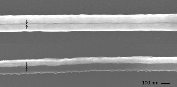
Figure 2. Scanning electron micrographs of the nanogaps produced using aluminum (top) and silver (bottom) as the spacer. Top image shows two layers of gold with the gap in between produced by etching out aluminum layer with aqueous HCl. Bottom image shows two layers of gold and aluminum with the gap produced by etching out silver layer with oxygen plasma. The gap is clearly visible in both cases.
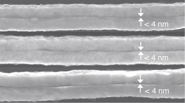
Figure 3. Scanning electron micrographs of the gaps of three different nanogap structures prepared using different dithiols as templates after ashing the organics with oxygen plasma. From top to bottom: nanogaps produced using SC12S, SC14S and SC16S that show a visible gap between gold layers. The nanogaps are qualitatively larger as the length of the molecules increases. All of the gap-widths are below the resolution limit of the instrument (~ 4 nm), thus they are labeled as ''< 4 nm."

Figure 4. Log current-density versus potential plots for nanogap structures fabricated from three different dithiols; SC12S (black squares), SC14S (red triangles), and SC16S (blue circles). The inset is a plot of ln(J) versus length (Å) at 500 mV showing a linear fit (R2 =0.99) with a slope corresponding to β = 0.75 Å-1 (0.94 nc-1).
Subscription Required. Please recommend JoVE to your librarian.
Discussion
In this paper we demonstrated the fabrication of nanogap structures using nanoskiving. This experimentally simple method enables the production of nanostructures at the rate of about one per second, with control over all three dimensions. The gap-size is defined by incorporating either sacrificial layers of aluminum and silver or self-assembled monolayers of dithiols (which affords a resolution as small as Å). The nanostructures can be positioned by hand on any arbitrary substrate and they are directly electrically addressable, which is a unique property of nanoskiving. This technique also produces highly uniform structures; however, very thin (< 50 nm) sections are sensitive to vibrations that alter the thickness of the individual structures. The quality of the diamond knife, which is the most important part of nanoskiving, is crucial to get continuous wires. Small nicks in the in knife result in scores in the final sections, while significant nicks in the knife produce broken wires. Sample mounting and alignment of the knife edge with the surface of the block requires some practice, but the technique requires no special training or skills and the nanofabrication process takes place entirely on the bench top, outside of a clean room.
Subscription Required. Please recommend JoVE to your librarian.
Disclosures
No conflicts of interest declared.
Acknowledgments
This work is part of the Joint Solar Programme (JSP) of Hyet Solar and the Stichting voor Fundamenteel Onderzoek der Materie FOM, which is part of the Netherlands Organization for Scientific Research (NWO).
Materials
| Name | Company | Catalog Number | Comments |
| Reagent/Material | |||
| Epofix epoxy resin | Electron Microscopy | 1232 | |
| Sciences | |||
| Gold | Schone Edelmetaal B.V | ||
| Aluminum | Umicore Materials AG | ||
| Silver | Umicore Materials AG | ||
| (tridecafluoro-1,1,2,2, | ABCR GmbH co.KG | 78560-45-9 | |
| -tetrahydrooctyl) | |||
| trichlorosilane | |||
| ,12-dodecanedithiol | Home-synthesised | According to: Akkerman et. al., Nature. 441, 69-72 (2006) | |
| ,14-tetradecanedithiol | synthesized in house | According to: Akkerman et. al., Nature. 441, 69-72 (2006) | |
| ,16-hexadecanedithiol | synthesized in house | According to: Akkerman et. al., Nature. 441, 69-72 (2006) | |
| Equipment | |||
| Thermal deposition system | home-built | ||
| Ultramicrotome | Leica Microsystems | ||
| Dimanod knife ultra 35 | Diatome | DU3540 | |
| Dimanod knife ultra 45 | Scimed GMBH | ||
| Scanning electron microscope | JOEL | ||
| Source meter | Keithley | ||
| Table 1. Tables of Specific Reagents and Equipment. | |||
References
- Lipomi, D. J., Martinez, R. V., Whitesides, G. M. Use of thin sectioning (nanoskiving) to fabricate nanostructures for electronic and optical applications. Angew. Chem. Int. Ed. 50 (37), 8566-8583 (2011).
- Xu, Q., Rioux, R. M., Dickey, M. D., Whitesides, G. M. Nanoskiving: A new method to produce arrays of nanostructures. Acc. Chem. Res. 41 (12), 1566-1577 (2008).
- Xu, Q., Rioux, R. M., Whitesides, G. M. Fabrication of complex metallic nanostructures by nanoskiving. ACS Nano. 1 (3), 215-227 (2007).
- Reed, M. A., Zhou, C., Muller, C. J., Burgin, T. P., Tour, J. M. Conductance of a molecular junction. Science. 278 (5336), 252-254 (1997).
- Chen, W., Ahmed, H., Nakazoto, K. Coulomb blockade at 77 k in nanoscale metallic islands in a lateral nanostructure. Appl. Phys. Let. 66 (24), 3383-3384 (1995).
- Morpurgo, A. F., Marcus, C. M., Robinson, D. B. Controlled fabrication of metallic electrodes with atomic separation. Appl. Phys. Let. 74 (14), 2084-2086 (1999).
- Paska, Y., Haick, H. Systematic cross-linking changes within a self-assembled monolayer in a nanogap junction: A tool for investigating the intermolecular electronic coupling. J. Am. Chem. Soc. 132 (6), 1774-1775 (2010).
- Park, J., Pasupathy, A. N., Goldsmith, J. I., Chang, C., Yaish, Y., Petta, J. R., Rinkoski, M., Sethna, J. P., Abruna, H. D., McEuen, P. L., Ralph, D. C. Coulomb blockade and the kondo effect in single-atom transistors. Nature. 417 (6890), 722-725 (2002).
- Nagase, T., Kubota, T., Mashiko, S. Fabrication of nano-gap electrodes for measuring electrical properties of organic molecules using a focused ion beam. Thin Solid Films. 438-439, 374-377 (2003).
- Kubatkin, S., Danilov, A., Hjort, M., Cornil, J., Brédas, J. -L., Stuhr-Hansen, N., Hedegård, P., Bjørnholm, T. Single-Electron Transistor of a Single Organic Molecule with Access to Several Redox States. Nature. 425 (6959), 698-701 (2003).
- Notargiacomo, A., Foglietti, V., Cianci, E., Capellini, G., Adami, M., Faraci, P., Evangelisti, F., Nicolini, C. Atomic force microscopy lithography as a nanodevice development technique. Nanotechnology. 10 (4), 458-463 (1999).
- Qin, L., Park, S., Huang, L., Mirkin, C. A. On-wire lithography. Science. 309 (5731), 113-115 (2005).
- Hatzor, A., Weiss, P. S. Molecular rulers for scaling down nanostructures. Science. 291 (5506), 1019-1020 (2001).
- Pourhossein, P., Chiechi, R. C. Directly addressable sub-3 nm gold nano-gaps fabricated by nanoskiving using self-assembled monolayers as templates. ACS Nano. 6, 5566-5573 (2012).
- Lipomi, D. J., Ilievski, F., Wiley, B. J., Deotare, P. B., Lončar, M., Whitesides, G. M. Integrated fabrication and magnetic positioning of metallic and polymeric nanowires embedded in thin epoxy slabs. ACS Nano. 3 (10), 3315-3325 (2009).
- Mays, R. L., Pourhossein, P., Savithri, D., Genzer, J., Chiechi, R. C., Dickey, M. D. Thiol-containing polymeric embedding materials for nanoskiving. Journal of Materials Chemistry C. , (2013).
- Thuo, M. M., Reus, W. F., Nijhuis, C. A., Barber, J. R., Kim, C., Schulz, M. D., Whitesides, G. M. Odd-even effects in charge transport across self-assembled monolayers. J. Am. Chem. Soc. 133 (9), 2962-2975 (2011).
- Song, H., Kim, Y., Jeong, H., Reed, M. A., Lee, T. Coherent Tunneling Transport in Molecular Junctions. J. Phys. Chem. C. 114 (48), 20431-20435 (2010).
- Wang, W. Y., Lee, T., Reed, M. A. Mechanism of Electron Conduction in Self-Assembled Alkanethiol Monolayer Devices. Phys. Rev. B. 68 (3), 035416 (2003).
- Weiss, E. A., Chiechi, R. C., Kaufman, G. K., Kriebel, J. K., Li, Z., Duati, M., Rampi, M. A., Whitesides, G. M. Influence of defects on the electrical characteristics of Mercury-Drop junctions: Self-Assembled monolayers of n- Alkanethiolates on rough and smooth. 129 (14), 4336-4349 (2007).
