

Summary
We describe key steps for biosensing by using polysilicon nanowire field-effect transistors, including the preparation of the device and the immobilization and confirmation of a DNA molecular probe on the nanowire surface, as well as conditions for DNA sensing.
Abstract
Surveillance using biomarkers is critical for the early detection, rapid intervention, and reduction in the incidence of diseases. In this study, we describe the preparation of polycrystalline silicon nanowire field-effect transistors (pSNWFETs) that serve as biosensing devices for biomarker detection. A protocol for chemical and biomolecular sensing by using pSNWFETs is presented. The pSNWFET device was demonstrated to be a promising transducer for real-time, label-free, and ultra-high-sensitivity biosensing applications. The source/drain channel conductivity of a pSNWFET is sensitive to changes in the environment around its silicon nanowire (SNW) surface. Thus, by immobilizing probes on the SNW surface, the pSNWFET can be used to detect various biotargets ranging from small molecules (dopamine) to macromolecules (DNA and proteins). Immobilizing a bioprobe on the SNW surface, which is a multistep procedure, is vital for determining the specificity of the biosensor. It is essential that every step of the immobilization procedure is correctly performed. We verified surface modifications by directly observing the shift in the electric properties of the pSNWFET following each modification step. Additionally, X-ray photoelectron spectroscopy was used to examine the surface composition following each modification. Finally, we demonstrated DNA sensing on the pSNWFET. This protocol provides step-by-step procedures for verifying bioprobe immobilization and subsequent DNA biosensing application.
Introduction
Silicon nanowire field-effect transistors (SNWFETs) have the advantages of ultra-high sensitivity and direct electrical responses to environmental charge variation. In n-type SNWFETs for example, when a negatively (or positively) charged molecule approaches the silicon nanowire (SNW), the carriers in the SNW are depleted (or accumulate). Consequently, the conductivity of the SNWFET decreases (or increases)1. Therefore, any charged molecule near the SNW surface of the SNWFET device can be detected. Vital biomolecules including enzymes, proteins, nucleotides, and many molecules on the cell surface are charge carriers and can be monitored using SNWFETs. With suitable modifications, particularly immobilizing a biomolecular probe on the SNW, a SNWFET can be developed into a label-free biosensor.
Surveillance using biomarkers is critical for diagnosing diseases. As shown in Table 1, several studies have used NWFET-based biosensors for label-free, ultra-high-sensitivity, and real-time detection of various biological targets, including a single virus2, adenosine triphosphate and kinase binding3, neuronal signals4, metal ions5,6, bacterial toxins7, dopamine8, DNA9-11, RNA12,13, enzyme and cancer biomarkers14-19, human hormones20, and cytokines21,22. These studies have demonstrated that NWFET-based biosensors represent a powerful detection platform for a broad range of biological and chemical species in a solution.
In SNWFET-based biosensors, the probe immobilized on the SNW surface of the device recognizes a specific biotarget. Immobilizing a bioprobe usually involves a series of steps, and it is critical that every step is properly performed to ensure the proper functioning of the biosensor. Various techniques have been developed for analyzing the surface composition, including X-ray photoelectron spectroscopy (XPS), ellipsometry, contact angle measurement, atomic force microscopy (AFM), and scanning electron microscopy (SEM). Methods such as AFM and SEM provide direct evidence of bioprobe immobilization on the nanowire device, whereas methods such as XPS, ellipsometry, and contact angle measurement are dependent on parallel experiments performed on other similar materials. In this report, we describe the confirmation of each modification step by using two independent methods. XPS is used to examine the concentrations of specific atoms on polysilicon wafers, and variations in the electric properties of the device are measured directly to confirm the charge variation on the SNW surface. We employ DNA biosensing by using polycrystalline SNWFETs (pSNWFETs) as an example to illustrate this protocol. Immobilizing a DNA probe on the SNW surface involves three steps: amine group modification on the native hydroxyl surface of the SNW, aldehyde group modification, and 5'-aminomodified DNA probe immobilization. At each modification step, the device can directly detect the variation in the charge of the functional group immobilized on the SNW surface, because the surface charges cause local interfacial potential changes over the gate dielectric that alter the channel current and conductance1. Charges surrounding the SNW surface can electrically modulate the electric properties of the pSNWFET device; therefore, the surface properties of the SNW play a crucial role in determining the electrical characteristics of pSNWFET devices. In the reported procedures, the immobilization of a bioprobe on the SNW surface can be directly determined and confirmed through electric measurement, and the device is prepared for biosensing applications.
Subscription Required. Please recommend JoVE to your librarian.
Protocol
1. Fabrication and Preservation of pSNWFET Devices
- Device Fabrication
Note: The pSNWFET was fabricated using a sidewall spacer technique as previously reported23,24.- Prepare the gate dielectric layer.
- Cap a 100-nm-thick thermal oxide (SiO2) layer on a Si substrate by using the wet oxidation process25 (O2 and H2 process gas at 980 °C for 4 hr).
- Deposit a 50-nm-thick nitride (Si3N4) layer by using low-pressure chemical vapor deposition (LPCVD)25 at 980 °C for 4 hr.
- Deposit a 100-nm-thick tetraethyl orthosilicate (TEOS) layer by using LPCVD25 at 780 °C for 4 hr.
- Perform standard lithography by using an I-line stepper to define the oxide dummy structures.
- Coat the wafer surface with an 830-nm-thick photoresist layer.
- Insert a pattern-defined photomask into the I-line stepper.
- Process the exposure by using the I-line stepper (wavelength: 365 nm) at a strength of 1,980 J at room temperature.
- Develop the wafer within a developer for 5 min.
- Perform the isotropic etching process by using a standard inductively coupled plasma25 etcher with HBr and Cl plasma gas for 1 min.
- Deposit a 100-nm-thick amorphous silicon (α-Si) layer by using LPCVD25.
- Perform an annealing step at 600 °C in N2 ambient for 24 hr to transform the α-Si into a polycrystalline structure.
- Implant phosphorous ions through source/drain (S/D) doping at low energy (5E15 cm−2)25.
- Perform standard lithography by using the I-line stepper to remove the poly-Si layer and form the polysilicon nanowire (pSNW)25.
Note: Repeat step 1.1.3 to implant dopants in places other than S/D regions with poly-Si removal and form the sidewall Si channels in a self-aligned manner. - Perform the passivation process (200-nm-thick TEOS oxide layer) by using LPCVD at 780 °C for 5 hr25.
- Perform standard lithography by using the I-line stepper to expose the nanowire channels, and form test pads by using the two-step dry/wet etching process.
- Repeat step 1.1.3.
- Perform the wet etching process (DHF: HF/H2O for 1 min).
- Prepare the gate dielectric layer.
- Wafer preservation
- Seal the wafer in a vacuum storage bag and store it in an electronic dry cabinet (relative humidity <40% at room temperature).
2. Pretreatment of the Device
- Device cleaning
- Rinse the device with pure acetone.
- Sonicate (46 kHz, 80 W) the device in pure acetone for 10 min.
- Sonicate (46 kHz, 80 W) the device in pure ethanol (99.5%) for 5 min.
- Blow-dry the surface of the device with nitrogen.
- Oxygen plasma
- Treat the device with O2 plasma at 18 W for 30 sec.
3. Immobilization of the DNA Probe on the Device Surface
- Amine group modification
- Immerse the device in a 2.0% (3-aminopropyl)triethoxysilane (APTES)/ethanol solution for 30 min.
- Wash the device with ethanol three times, and then sonicate (46 kHz, 80 W) the device in ethanol for 10 min.
- Heat the device on a hot plate at 120 °C for 10 min to create amine groups on SNWs.
- Aldehyde group modification
- Immerse the device in 12.5% glutaraldehyde for 1 hr at room temperature to create aldehyde groups on the surface. Avoid light exposure.
- Wash the device with 10 mM sodium phosphate buffer (Na-PB; pH 7.0) three times, and then blow-dry the surface of the device with nitrogen.
- DNA probe immobilization
- Immerse the device in a solution containing 1 µM DNA probes overnight.
- Immerse the device in 10 mM Tris buffer (pH 8.0) with 4.0 mM NaBH3CN for 30 min to block the unreacted aldehyde groups.
- Wash the device with Na-PB (pH 7.0) three times, and then blow-dry the surface of the device with nitrogen.
4. Confirmation and Analysis of Surface Modification on pSNWFET
- pH profile following each step of surface modification
- Prepare 10 mM Na-PB in pH 3.0-9.0.
- Prepare 10 mM sodium phosphate tribasic dodecahydrate (Na3PO4) in deionized water (pH 11.60).
- Prepare 10 mM phosphoric acid (H3PO4) in deionized water (pH 2.35).
- Place the pH electrode into 500 ml of 10 mM Na3PO4 buffer, and mix this solution with different volumes of 10 mM H3PO4 buffer while measuring the pH value to obtain buffers with pH values of 3.0, 4.0, 5.0, 6.0, 7.0, 8.0, and 9.0.
- AC conductance measurement
Note: The measurement circuit included a small AC signal generator and an Au microwire that served as the liquid gate electrode.- Determine the optimal liquid gate voltage (VLG) for measurement26 at each modification step (steps 2.2, 3.1, 3.2, and 3.3).
Note: The electric properties of the device after four surface modifications on the SNW were measured as described in this section. In step 2.2, the unmodified pSNWFET containing the native oxide layer is modified; step 3.1 entails modifying the device with the amine group of APTES; step 3.2 involves modification with the uncharged functional group of glutaraldehyde; and step 3.3 involves DNA probe modification.- Deliver the 10 mM Na-PB (pH 7.0) solution to the SNW surface by using a syringe pump (flow rate: 5.0 ml/hr) for direct contact with the SNW.
- Measure the real-time conductance of the device while sweeping VLG from 0.80 to 1.30 V.
- Perform conductance measurement by using the lock-in technique27 at room temperature.
- Convert the AC current signals into an AC voltage signal by using a low-noise current preamplifier.
- Collect data on conductance (G) upon increasing VLG from 0.80 to 1.30 V (interval = 0.02 V).
- Determine the optimal VLG (most sensitive VLG) of the device26.
- Plot the G-VLG curves from step 4.1.2.1.2.3 to obtain the equation of the curve.
- Differentiate the equation, and calculate the values in each point of VLG.
- Divide the value from step 4.1.2.1.3.2 by G, and determine the optimal VLG according to the maximum number.
- Measure the real-time conductance of the pH profile at each step of the surface modification.
- Perform conductance measurement by using the lock-in technique27 at room temperature.
- Convert the AC current signal into AC voltage signals by using a low-noise current preamplifier.
- Set the optimal VLG for each step of surface modification (step 2.2: VLG = 1.02, step 3.1: VLG = 0.98, step 3.2: VLG = 0.98, and step 3.3: VLG = 1.0).
- Deliver the 10 mM Na-PB solution with pH values from 3.0 to 9.0 to the SNW surface (flow rate: 5.0 ml/hr), and collect the data on conductance at a drain voltage of 0.01 V.
- Determine the optimal liquid gate voltage (VLG) for measurement26 at each modification step (steps 2.2, 3.1, 3.2, and 3.3).
- Prepare 10 mM Na-PB in pH 3.0-9.0.
- Measurement of electric properties (the ID-VBG curve) of the device in 10 mM Na-PB (pH 7.0) following each step of surface modification (steps 2.2, 3.1, 3.2, and 3.3.)
Note: The electric properties of the device after four surface modifications on the SNW were measured: in step 2.2, the unmodified pSNWFET containing the native oxide layer is modified; step 3.1 involves modifying the device with the amine group of APTES; step 3.2 entails modification with the uncharged functional group of glutaraldehyde; and step 3.3 entails DNA probe modification.- Deliver the 10 mM Na-PB (pH 7.0) solution to the SNW surface (steps 2.2, 3.1, 3.2, and 3.3) by using a syringe pump (flow rate: 5.0 ml/hr) for direct contact with the SNW.
- Measure the ID of the device (steps 2.2, 3.1, 3.2, and 3.3) by using a commercial semiconductor analyzer and software.
- Select the "nMOSFET" mode.
- Select "ID-VBG" modules.
Note: ID is the drain/source current, and VBG is the back gate voltage. - Set a constant bias voltage (VD = 0.5 V) while sweeping the gate potential (VBG) from −1 to 3.0 V (interval = 0.2 V).
- Click the Run icon to obtain ID-VBG curves.
5. DNA Biosensing
Note: In a typical experiment, the ID-VBG curve is determined three times to ensure that no further variation is observed.
- Determination of the baseline
- Deliver the 10 mM Na-PB solution (pH 7.0) to the DNA probe-immobilized SNW surface for 10 min by using a syringe pump (flow rate: 5.0 ml/hr), and then incubate the SNW for 30 min.
- Measure the ID of the device (repeat step 4.2.2).
- Sensing of DNA/DNA hybridization
- Load 10 pM complementary target DNA onto the DNA probe-immobilized SNW surface for 10 min by using a syringe pump (flow rate: 5.0 ml/hr), and then incubate the SNW for 30 min.
- Deliver the 10 mM Na-PB solution (pH 7.0) onto the SNW surface for 10 min by using a syringe pump (flow rate: 5.0 ml/hr) to wash the unbound target DNA away.
- Repeat step 4.2.2 to measure the ID of the device.
- Reconfirm the signal of DNA/DNA hybridization.
- Load 1 nM recovery DNA onto the DNA probe-immobilized SNW surface for 10 min by using a syringe pump (flow rate: 5.0 ml/hr), and then incubate the SNW for 30 min.
- Deliver the 10 mM Na-PB solution (pH 7.0) onto the SNW surface for 10 min by using a syringe pump (flow rate: 5.0 ml/hr).
- Repeat step 4.2.2 to measure the ID of the device.
- Negative control
- Load 100 pM non-complementary DNA onto the DNA probe-immobilized SNW surface for 10 min by using a syringe pump (flow rate: 5.0 ml/hr), and then incubate the SNW for 30 min.
- Deliver the 10 mM Na-PB solution (pH 7.0) onto the SNW surface for 10 min by using a syringe pump (flow rate: 5.0 ml/hr).
- Repeat step 4.2.2 to measure the ID of the device.
Subscription Required. Please recommend JoVE to your librarian.
Representative Results
Various SNWFETs have been reported to serve as transducers of biosensors (Table 1). Single-crystalline SNWFETs (sSNWFETs) and pSNWFETs show comparable electric properties as transducers in aqueous solutions, and both have been reported to have many biosensing applications. An advantageous feature of the pSNWFET device used in this study is its simple and low-cost fabrication procedure. Figure 1a shows the key steps involved in fabricating the pSNWFET. An optical image of a die from the 6-inch wafer (Figure 1b) and SEM images (Figure 1c) of a single device (two SNWs, approximately 100 nm in width and 1.6 μm in length) were obtained.
Figure 2a illustrates the procedure of DNA probe immobilization on the SNW surface. Each modification step was confirmed using XPS (Figure 2b). The pH profiles for real-time conductance (Figure 2c, d) are shown at various stages of SNW surface modification. For the unmodified pSNWFET containing the native oxide layer on the SNW surface, the hydroxyl groups (-OH) were ionized to form charged groups (-O−) with increasing pH values (black line). The decrease in conductance at pH 6.0 to 9.0 indicates that the acid dissociation constant (pKa) of the hydroxyl group can be set to approximately 7.0. Conductance likely increases at pH 3.0 to 6.0 because of the increase in the ionic strength, affecting device characteristics1. After the APTES modification, the response to the conductance of the APTES-modified device showed high variation (red line). The amine group (pKa = 4.0) of APTES can be protonated at a low pH to produce a positive charge28. Thus, the SNW conductance decreased with discrete changes in pH values from 3.0 to 9.0. After the SNW was modified with glutaraldehyde, the response was relatively stable for conductance at pH ranging from 3.0 to 9.0 (blue line). This may be attributed to the uncharged functional group that is insensitive to the change in pH environments. Finally, after the negatively charged DNA probe was immobilized, conductance slightly decreased with an increase in pH values (green line).
The shift in the electric properties of the device (Figure 2e) with different modifications confirms the change in the SNW surface. In such experiments, the ID-VG curve of the unmodified pSNWFET was used as the baseline (black line). After the SNW was immersed in APTES, the ID-VG curve of the device shifted to the left (increased current) because of the positive charge on the SNW surface caused by the amino group on APTES (black to red line). After conjugation of glutaraldehyde to the APTES-modified device, the ID-VG curve shifted back to the right because of imide bond formation. The current decreased because the positively charged amine was converted to neutrally charged imide (red to blue line). Finally, the 5'-amnimodified DNA probe was introduced to bind to the APTES-glutaraldehyde-modified device. The sugar-phosphate backbone of DNA caused the ID-VG curve to shift to the far right (blue to green line), which is consistent with the effect of negative ions on n-type FET.
The detection of DNA/DNA hybridization on the pSNWFET is shown in Figure 3. The probe, target, recovery, and noncomplementary DNA sequences designed for detecting the avian influenza virus (AIV)29,30 are shown in Table 2. The ID-VG curve of the DNA probe-modified pSNWFET obtained in 10 mM Na-PB (pH 7.0) was used as the baseline (black). Subsequently, 10 pM target DNA was introduced to hybridize with the immobilized DNA probe on the SNW surface, and a clear decrease in the drain current of the device was observed (red line). The decreased ID in the n-type SNWFET implied an increased negative charge (caused by the phosphate backbone) on the SNW surface. Recovery DNA was designed to rehybridize with the target DNA and free the DNA probe31. If the recovery DNA is properly designed, the reaction thermodynamically favors the rehybridization of the target-recovery DNA duplex, because more complementary nucleotides are available between these two DNA strands (Table 1) than those between the probe and target DNA. Adding 1 nM recovery DNA (blue line) further confirmed that the electric response of the target DNA was due to the hybridization of the probe-target DNA and freed the DNA probe, which is reusable for subsequent experiments. As a negative control, noncomplementary DNA [AIV subtype H5 target DNA] (100 pM) was also injected and mixed with the DNA probe, and the ID-VG curve remained unchanged. The DNA probe immobilized on the pSNWFET is insensitive to noncomplementary DNA. Only target DNA causes an appreciable shift in the ID-VG curve. The ID-VG curve returns to the baseline following incubation with the recovery DNA.
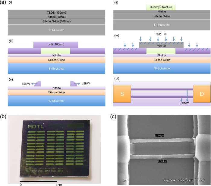
Figure 1. Preparation of the pSNWFET device. (a) Scheme of device fabrication. (i) A 6-inch Si wafer was capped with a 100-nm-thick thermal oxide layer. Next, 50-nm-thick nitride and 100-nm-thick TEOS layers were deposited as starting materials by using LPCVD. (ii) A TEOS dummy structure was defined and formed using standard lithography; two insulator layers (oxide and nitride) served as the gate dielectric. (iii) A 100-n-thick α-Si layer was deposited using LPCVD, and annealing was subsequently conducted to transform the α-Si into poly-Si. (iv) S/D doping was then performed through phosphorus ion implantation. (v) The sidewall Si channels were formed in a self-aligned manner by using standard lithography. (vi) Top view of the fabricated device structure with pSNW. (b) Optical images of a pSNWFET biosensor chip. (c) SEM image of a single pSNWFET device. Please click here to view a larger version of this figure.
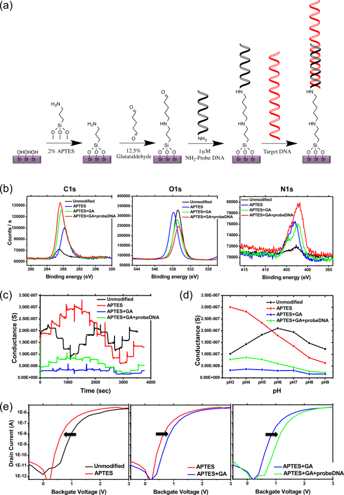
Figure 2. Surface modification and validation on pSNWFET. (a) Scheme of surface functionalization of DNA and DNA/DNA hybridization. (b) XPS spectra of C1s, O1s, and N1s signals from the silicon wafer (sampling depth = 7.5 nm), where the sequential stepwise surface modification of the immobilized DNA probe was performed. High-resolution spectra were obtained, and the overall energy resolution was set to 0.1 eV. (c) Real-time curve at various pH values at each step of the surface modification; 10 mM Na-PB was injected in the following order: pH 7.0 → pH 6.0 → pH 5.0 → pH 4.0 → pH 3.0 → pH 4.0 → pH 5.0 → pH 6.0 → pH 7.0 → pH 8.0 → pH 9.0 → pH 8.0 → pH 7.0. (d) Average conductance at pH values from 3.0 to 9.0 with 10 mM Na-PB following each step of surface modification. (e) Electric properties (ID-VBG curves) of the pSNWFET at each step of surface modification. Please click here to view a larger version of this figure.
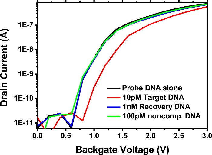
Figure 3. DNA biosensing on pSNWFET. The ID-VG curves of the DNA probe-modified pSNWFET were obtained in 10 mM Na-PB (pH 7) (black line). The ID-VG curve following hybridization of the probe and target DNA (red line) was obtained by introducing 10 pM target DNA and washing it with 10 mM Na-PB (pH 7). The DNA probe (blue line) was recovered by adding 1 nM recovery DNA to remove the target DNA. Noncomplementary DNA was used as negative control in this experiment (green line).
| Bio-target | Sensitivity | Crystalline | Type | Reference |
| pH | single | p | 35 | |
| Cystic fibrosis ∆F508 | 3 bases deletion | single | p | 9 |
| Influenza A | single virus | single | p | 2 |
| ATP sensing | 100 pM | single | p | 3 |
| Telomerase | 10 Hela cell | single | p | 14 |
| PSA / CEA / Mucin-1 | <1.4 / 2 / 5 pg/ml | single | n/p | 14 |
| Neuronal signal | single | n/p | 4 | |
| Ca2+ | 100 nM | single | n | 5 |
| Bacterial toxin (SEB) | 10 fM | poly | p | 7 |
| Dopamine | 1 fM | poly | n | 8 |
| Troponin-T | 1 fg/ml | single | n | 19 |
| Vascular endothelial growth factor | 1.04 / 0.104 nM | single | n/p | 18 |
| BRAFV599E | 1-base-mismatch | single | n | 11 |
| AIV DNA | 1 fM | poly | n | 10 |
| Avidin / streptavidin | 1.48 nM / 167 fM | poly | n | 37 |
| Ca2+ / Troponin I | 1 μM / 7 nM | single | p | 6 |
| Dengue serotype 2 RNA | <10 fM | single | n | 12 |
| CaM protein Kinase | expressed cell lysate | single | p | 16 |
| Matrix metalloproteinase-2 | 100 fM | single | p | 15 |
| MicroRNAs (miR-21 / miR-205) | 1 zeptomole (ca. 600 copies) | single | p | 13 |
| Vascular endothelial growth factor | 1.25 pg/ml | poly | n | 21 |
| Human thyroid stimulating hormone | 0.11 pM | single | n | 20 |
| Apolipoprotein A II protein | 6.7 pg/ml | poly | n | 17 |
| Interleukin 8 / tumor necrosis factor α | 10 fg/ml | single | n | 22 |
Table 1. Partial list of biotargets examined using SNWFET devices.
| Oligonucleotides | Sequence |
| AIV H1 5’-aminomodified probe DNA | 5’-NH2-C6-CACACTCTGTCAACCTAC-3’ |
| AIV H1 target DNA | 5’-CCATTGTGACTGTCCTCAAGTAGGTTGACAGAGTGTG-3’ |
| AIV H1 recovery DNA | 5’-CACACTCTGTCAACCTACTTGAGGACAGTCACAATGG-3’ |
| Non-complementary DNA (AIV H5 target DNA) | 5’-TGATAACCAATGCAGATTTG-3’ |
Table 2. Sequences of synthetic oligonucleotides.
Subscription Required. Please recommend JoVE to your librarian.
Discussion
Commercializing the top-down and bottom-up fabrication approaches for sSNWFETs is considered difficult because of its cost32,33, SNW position control34,35, and its low production scale36. By contrast, fabricating pSNWFETs is simple and low cost37. Through the top-down approach and combination with the sidewall spacer formation technique (Figure 1), the size of the SNW can be controlled by adjusting the duration of reactive plasma etching. The procedures for preparing the nanowires of the pSNWFET illustrated in Figure 1a can be easily adapted to commercial semiconductor facilities. Consequently, pSNWFETs have several advantages including cost effectiveness, a simple construction technique, and a CMOS-compatible fabrication process and thus can be applied in biosensing.
In contrast to the fabrication of the semiconductor device, a process well defined in commercial facilities, the immobilization of the bioprobe on the device may vary for each specific application. The immobilization of the DNA probe on the SNW surface is illustrated in Figure 2a as an example. Other bioprobes, such as antibodies, aptamers, and enzymes, can also be immobilized on the SNW surface for detecting different targets. The following steps are critical for successfully immobilizing the DNA probe. In our protocol, the as-fabricated pSNWFET device is cleaned and treated with oxygen plasma and then immersed in an APTES/ethanol solution to create amine groups on the SNWs. Next, the device is immersed in a glutaraldehyde solution to create aldehyde groups on the surface. These groups are later conjugated to the 5'-aminomodified DNA probe. Multiple-step conjunctions between cross-linker molecules and the bioprobe were required to transform the semiconductor device to a biosensor. Thus, it is crucial to ensure that every step is successful. At each step of DNA probe immobilization, XPS was used to analyze and confirm the composition and chemistry of the surface. The atomic concentrations of carbon, oxygen, and nitrogen were determined on the basis of XPS scans of the respective peaks, as shown in Figure 2b. Upon addition of the DNA probe, the most notable changes were an increase in carbon and nitrogen concentrations. An increasing trend was observed in the carbon and nitrogen concentrations at each step of the DNA probe immobilization procedure. The oxygen concentration decreased during the procedure because the native hydroxyl group became covered through surface modification. These results revealed that the DNA probe was immobilized, which is consistent with the change in electric properties, as shown in Figure 2c, d, and e. The aforementioned procedures are useful for troubleshooting in case of unsuccessful surface modification. However, they are usually performed on a separate wafer coated with a material similar to that on the nanowire surface. Direct evidence of changes in the electric properties of the modified device is required to confirm the outcome of surface modification on the device, as described in the following paragraphs.
One of the most frequently used methods for directly monitoring changes in the FET device surface is pH sensing, as shown in Figure 2d and d. Different surface modifications result in variation in the charge on the SNW surface, greatly affecting the surface potential of the pSNWFET under different environments. We used broad-range pH buffer solutions to detect changes in conductance corresponding to the functional groups on the SNW surface. From a mechanistic perspective, the increase in conductance with changing pH (increase in hydrogen ions) is consistent with the increase in the positive surface charge, which "turns on" the n-type FET through the accumulation of electrons. The real-time electric responses to the conductance of the pSNWFET can be measured in buffer solutions with pH values ranging from 3.0 to 9.0. The methods described in this report are useful for examining whether a semiconductor-based sensor is prepared for biosensing application.
Figure 2e illustrates a convenient method for determining the outcome of the surface modification through direct measurement of the electric properties of the device. The changes in ID-VG curves shown in Figure 2e are consistent with each stage of DNA probe immobilization on the SNW surface. According to the results, pSNWFETs can be directly used to confirm the procedure at each step of bioprobe immobilization. This result also indicates that the modified pSNWFET is prepared for biosensing application. These procedures are particularly useful when the immobilization procedures are well established. The function of a pSNWFET-based biosensor was examined by detecting AIV subtype H1 DNA as an example (Figure 3). Using probe and target DNA is suitable for illustrating the development of a novel biosensor because of the stability of the DNA molecules and the techniques available for easily obtaining the desired DNA sequence. In addition to using noncomplementary DNA as a negative control, we demonstrated DNA hybridization on the pSNWFET with a recovery system. This is particularly useful when a new system or new device is used for biosensing experiments. Many steps are involved in the process from device fabrication to biosensing application. Each step affects the final outcome. Furthermore, false positive or false negative results are usually obtained in biosensing experiments because of the complexity of the biosensing environment. Thus, controlled experiments are critical, and the recovery system demonstrated in this study can greatly facilitate identifying unexpected factors that interfere with the experimental results.
The main limitations for currently used pSNWFET-based biosensor are the availability of the pSNWFET device and the instrumentation used for measurement. However, these two limitations can be easily overcome in the near future. Many types of SNWFETs have been reported in the literature. The pSNWFET demonstrated in this study is already being fabricated using the standard semiconductor process and can be mass produced with only minor adjustments to the commercial wafer fabrication process. The instrumentation used for measurement in this study was a standard semiconductor chip analyzer. This implies that, with a proper integrated circuit installed on the device, portable instrumentation can be designed and manufactured using current electronic technology.
In conclusion, we describe the complete procedure for DNA sensing on a pSNWFET. Because the immobilization procedure strongly affects the ability of a biosensor to effectively detect biomolecules, this protocol provides step-by-step confirmation of bioprobe immobilization and the readiness of the device for DNA biosensing applications. Similar procedures can be adapted from this report for many similar biosensing applications, for which adjustments are necessary. This report also describes protocols for confirming and troubleshooting of the immobilization of the bioprobe and device surface modifications. The demand for various biosensors is increasing. The methods described in this report are an appropriate reference for preparing and developing semiconductor-based biosensors.
Subscription Required. Please recommend JoVE to your librarian.
Disclosures
The authors have nothing to disclose.
Acknowledgments
This research was financially supported by Ministry of Science and Technology, Taiwan (104-2514-S-009 -001, 104-2627-M-009-001 and 102-2311-B-009-004-MY3). We thank the National Nano Device Laboratories (NDL) for its valuable assistance during device fabrication and analysis.
Materials
| Name | Company | Catalog Number | Comments |
| Acetone | ECHO | AH-3102 | |
| (3-Amonopropyl)triethoxysilane (APTES), ≥98% | Sigma-Aldrich | A3648 | Danger |
| Ethanol, anhydrous, 99.5% | ECHO | 484000203108A-72EC | |
| Glutaraldehyde solution (GA), 50% | Sigma-Aldrich | G7651 | Avoid light |
| Sodium cyanoborohydride, ≥95.0% | Fluka | 71435 | Danger and deliquescent |
| Sodium phosphate tribasic dodecahydrate, ≥98% | Sigma | 04277 | |
| Phosphoric acid, ≥99.0% | Fluka | 79622 | Deliquescent |
| Photoresist (iP3650) | Tokyo Ohka Kogyo Co., LTD | THMR-iP3650 HP | |
| Synthetic oligonucleotides, HPLC purified | Protech Technology | ||
| Tris(hydroxymethyl)aminomethane (Tris), ≥99.8% | USB | 75825 | |
| Keithley 2636 System SourceMeter | Keithley | ||
| SR830 DSP Lock-In Amplifier | Stanford Research Systems | ||
| SR570 Low-noise Current Preamplifier | Stanford Research Systems | ||
| Ni PXI Express | National Instruments |
References
- Lin, C. H., et al. Surface composition and interactions of mobile charges with immobilized molecules on polycrystalline silicon nanowires. Sensor Actuat B-Chem 211. 211, 7-16 (2015).
- Patolsky, F., et al. Electrical detection of single viruses. P Natl Acad Sci USA. 101, 14017-14022 (2004).
- Wang, W. U., Chen, C., Lin, K. H., Fang, Y., Lieber, C. M. Label-free detection of small-molecule-protein interactions by using nanowire nanosensors. P Natl Acad Sci USA. 102, 3208-3212 (2005).
- Patolsky, F., et al. Detection, stimulation, and inhibition of neuronal signals with high-density nanowire transistor arrays. Science. 313, 1100-1104 (2006).
- Bi, X., et al. Development of electrochemical calcium sensors by using silicon nanowires modified with phosphotyrosine. Biosens Bioelectron. 23, 1442-1448 (2008).
- Lin, T. W., et al. Label-free detection of protein-protein interactions using a calmodulin-modified nanowire transistor. P Natl Acad Sci USA. 107, 1047-1052 (2010).
- Mishra, N. N., et al. Ultra-sensitive detection of bacterial toxin with silicon nanowire transistor. Lab on a chip. 8, 868-871 (2008).
- Lin, C. H., et al. Ultrasensitive detection of dopamine using a polysilicon nanowire field-effect transistor. Chem Commun. , 5749-5751 (2008).
- Hahm, J., Lieber, C. M. Direct ultrasensitive electrical detection of DNA and DNA sequence variations using nanowire nanosensors. Nano Lett. 4, 51-54 (2004).
- Lin, C. H., et al. Poly-silicon nanowire field-effect transistor for ultrasensitive and label-free detection of pathogenic avian influenza DNA. Biosens Bioelectron. 24, 3019-3024 (2009).
- Wu, C. C., et al. Label-free biosensing of a gene mutation using a silicon nanowire field-effect transistor. Biosens Bioelectron. 25, 820-825 (2009).
- Zhang, G. -J., et al. Silicon nanowire biosensor for highly sensitive and rapid detection of Dengue virus. Sensor Actuat B-Chem. 146, 138-144 (2010).
- Lu, N., et al. CMOS-compatible silicon nanowire field-effect transistors for ultrasensitive and label-free microRNAs sensing. Small. 10, 2022-2028 (2014).
- Zheng, G., Patolsky, F., Cui, Y., Wang, W. U., Lieber, C. M. Multiplexed electrical detection of cancer markers with nanowire sensor arrays. Nat Biotechnol. 23, 1294-1301 (2005).
- Choi, J. H., Kim, H., Choi, J. H., Choi, J. W., Oh, B. K. Signal enhancement of silicon nanowire-based biosensor for detection of matrix metalloproteinase-2 using DNA-Au nanoparticle complexes. ACS Appl Mater Interfaces. 5, 12023-12028 (2013).
- Lin, T. Y., et al. Improved silicon nanowire field-effect transistors for fast protein-protein interaction screening. Lab Chip. 13, 676-684 (2013).
- Chen, H. C., et al. A sensitive and selective magnetic graphene composite-modified polycrystalline-silicon nanowire field-effect transistor for bladder cancer diagnosis. Biosens Bioelectron. 66, 198-207 (2015).
- Lee, H. S., Kim, K. S., Kim, C. J., Hahn, S. K., Jo, M. H. Electrical detection of VEGFs for cancer diagnoses using anti-vascular endotherial growth factor aptamer-modified Si nanowire FETs. Biosens Bioelectron. 24, 1801-1805 (2009).
- Chua, J. H., Chee, R. E., Agarwal, A., Wong, S. M., Zhang, G. J. Label-free electrical detection of cardiac biomarker with complementary metal-oxide semiconductor-compatible silicon nanowire sensor arrays. Anal Chem. 81, 6266-6271 (2009).
- Lu, N., et al. Label-free and rapid electrical detection of hTSH with CMOS-compatible silicon nanowire transistor arrays. ACS Appl Mater Interfaces. 6, 20378-20384 (2014).
- Chen, H. C., et al. Magnetic-composite-modified polycrystalline silicon nanowire field-effect transistor for vascular endothelial growth factor detection and cancer diagnosis. Anal Chem. 86, 9443-9450 (2014).
- Zhang, Y. L., et al. Silicon Nanowire Biosensor for Highly Sensitive and Multiplexed Detection of Oral Squamous Cell Carcinoma Biomarkers in Saliva. Anal Sci. 31, 73-78 (2015).
- Lin, H. C., et al. A simple and low-cost method to fabricate TFTs with poly-Si nanowire channel. Ieee Electr Device L. 26, 643-645 (2005).
- Lin, H. C., Lee, M. H., Su, C. J., Shen, S. W. Fabrication and characterization of nanowire transistors with solid-phase crystallized poly-Si channels. Ieee T Electron Dev. 53, 2471-2477 (2006).
- Doering, R., Nishi, Y. Handbook of semiconductor manufacturing technology. , 2nd, CRC Press. (2008).
- Lu, M. P., Hsiao, C. Y., Lai, W. T., Yang, Y. S. Probing the sensitivity of nanowire-based biosensors using liquid-gating. Nanotechnology. 21 (425505), (2010).
- Gaspar, J., et al. Digital lock in amplifier: study, design and development with a digital signal processor. Microprocess Microsy. 28, 157-162 (2004).
- Vezenov, D. V., Noy, A., Rozsnyai, L. F., Lieber, C. M. Force titrations and ionization state sensitive imaging of functional groups in aqueous solutions by chemical force microscopy. J Am Chem Soc. 119, 2006-2015 (1997).
- Townsend, M. B., et al. Experimental evaluation of the FluChip diagnostic microarray for influenza virus surveillance. J Clin Microbiol. 44, 2863-2871 (2006).
- Wang, L. C., et al. Simultaneous detection and differentiation of Newcastle disease and avian influenza viruses using oligonucleotide microarrays. Vet Microbiol. 127, 217-226 (2008).
- Lin, C. -H., et al. Recovery Based Nanowire Field-Effect Transistor Detection of Pathogenic Avian Influenza DNA. Jpn J Appl Phys. 51 (02BL02), (2012).
- Lee, K. N., et al. Well controlled assembly of silicon nanowires by nanowire transfer method. Nanotechnology. 18 (445302), (2007).
- Li, Z., et al. Sequence-specific label-free DNA sensors based on silicon nanowires. Nano Lett. 4, 245-247 (2004).
- McAlpine, M. C., et al. High-performance nanowire electronics and photonics on glass and plastic substrates. Nano Lett. 3, 1531-1535 (2003).
- Cui, Y., Wei, Q., Park, H., Lieber, C. M. Nanowire nanosensors for highly sensitive and selective detection of biological and chemical species. Science. 293, 1289-1292 (2001).
- Patolsky, F., Zheng, G., Lieber, C. M. Nanowire-based biosensors. Anal Chem. 78, 4260-4269 (2006).
- Hsiao, C. Y., et al. Novel poly-silicon nanowire field effect transistor for biosensing application. Biosens Bioelectron. 24, 1223-1229 (2009).
