Quantum integrated circuits (QICs) consisting of array of planar and ballistic Josephson junctions (JJs) based on In0.75Ga0.25As two-dimensional electron gas (2DEG) is demonstrated. Two different methods for fabrication of the two-dimensional (2D) JJs and QICs are discussed followed by the demonstration of quantum transport measurements in sub-Kelvin temperatures.
Method Article
Scalable Quantum Integrated Circuits on Superconducting Two-Dimensional Electron Gas Platform
In This Article
Summary
Abstract
To form a coherent quantum transport in hybrid superconductor-semiconductor (S-Sm) junctions, the formation of a homogeneous and barrier-free interface between two different materials is necessary. The S-Sm junction with high interface transparency will then facilitate the observation of the induced hard superconducting gap, which is the key requirement to access the topological phases (TPs) and observation of exotic quasiparticles such as Majorana zero modes (MZM) in hybrid systems. A material platform that can support observation of TPs and allows the realization of complex and branched geometries is therefore highly demanding in quantum processing and computing science and technology. Here, we introduce a two-dimensional material system and study the proximity induced superconductivity in semiconducting two-dimensional electron gas (2DEG) that is the basis of a hybrid quantum integrated circuit (QIC). The 2DEG is a 30 nm thick In0.75Ga0.25As quantum well that is buried between two In0.75Al0.25As barriers in a heterostructure. Niobium (Nb) films are used as the superconducting electrodes to form Nb- In0.75Ga0.25As -Nb Josephson junctions (JJs) that are symmetric, planar and ballistic. Two different approaches were used to form the JJs and QICs. The long junctions were fabricated photolithographically, but e-beam lithography was used for short junctions’ fabrication. The coherent quantum transport measurements as a function of temperature in the presence/absence of magnetic field B are discussed. In both device fabrication approaches, the proximity induced superconducting properties were observed in the In0.75Ga0.25As 2DEG. It was found that e-beam lithographically patterned JJs of shorter lengths result in observation of induced superconducting gap at much higher temperature ranges. The results that are reproducible and clean suggesting that the hybrid 2D JJs and QICs based on In0.75Ga0.25As quantum wells could be a promising material platform to realize the real complex and scalable electronic and photonic quantum circuitry and devices.
Introduction
A Josephson junction (JJ) is formed by sandwiching a thin layer of a non-superconducting (normal) material between two superconductors1. Various novel quantum electronic and photonic circuits and devices can be built based on JJs2,3,4,5,6,7,8,9,10,11,12,13,14,15,16. Among them, the JJs with semiconductor as their non-superconducting (normal) part, or superconductor-semiconductor-superconductor (S-Sm-S) JJs, have received much attention in recent years after the purported detection of exotic Majorana particles with zero electrical charges at the interface of a superconductor and a semiconducting one-dimensional (1D) nanowire17,18,19,20,21,22. Nanowire-based hybrid devices are limited to the 1D geometry of the nanowire and fabrication of Y and/or T-structures out of them - a necessary requirement for Majorana braiding- is challenging22. The fine tuning of nanowire’s chemical potential, for accessing topological phases, requires JJs with several electrostatically gates which causes quite a lot of issues in complex device fabrication out of nanowires. To overcome the scalability issues of 1D wires, two-dimensional (2D) material platforms are highly desirable19,22.
Among 2D materials, the two-dimensional electron gas (2DEG) platform -forms when electrons are confined to an interface between two different materials in a semiconductor heterostructure- is the most promising candidate22. The combination of 2DEG with superconductors and forming hybrid 2D JJs opens a new avenue towards the development of next-generation scalable quantum systems such as topological quantum processing and computing. They can support phase coherent quantum transport, and proximity induced superconductivity with high transmission probability, which are fundamental requirement for topological phase observation. In this regard, we demonstrate a QIC on a chip which consists of array of ballistic 2D JJs that can be controlled by 20 wires. Each junction has two Nb electrodes as the superconducting part and In0.75Ga0.25As quantum wells in a semiconducting heterojunction as the normal part. The wafer can be easily patterned to form complex structures and networked QICs.
The advantages of In0.75Ga0.25As 2DEG include: (i) relatively large g-factor, (ii) strong Rashba spin-orbit coupling, (iii) the low electron effective mass, and (iv) that the indium composition can be tuned allowing the formation of JJs with high interface transparency23,24,25. The wafer can be grown as a disk of up to 10 cm dimeter, allowing fabrication of thousands of hybrid 2D JJs and complex QICs networks so overcoming the scalability challenges of these quantum devices.
We discuss two different approaches for device fabrications: For device 1, a circuit which includes eight identical and symmetric JJs of 850 nm length and 4 μm widths are patterned by photolithography23,24. The device 2 includes eight junctions with different lengths. They all have the same width of 3 μm. The JJs are patterned by e-bam lithography25. The transport measurements at sub-Kelvin temperature ranges in absence/presence of magnetic field will be presented. The on-chip QICs consists of array of 2D Nb- In0.75Ga0.25As -Nb JJs. The long and short junctions are measured in a dilution fridge with a base temperature of 40 mK and liquid 3He cooled cryostat with a base temperature of 300 mK, respectively. Devices are biased with an ac-signal of 5 μV at 70 Hz which is superimposed to the junction dc voltage bias. A two-terminal standard lock-in technique is used to measure the device output ac-current23,24,25.
Protocol
NOTE: Semiconductor heterostructure and hybrid S-Sm Josephson junction fabrication are presented.
1. Semiconducting heterostructure fabrication
NOTE: The molecular beam epitaxy (MBE) grown In0.75Ga0.25As quantum wells are used in this study23,24,25,26. Figure 1 depicts the sequence of distinct layers:
- Clean a 500 μm thick, 3-inch semi-insulating (001) GaAs substrate and remove the oxide layer in high temperature (above 200 °C)26.
- Adjust the growth temperature at 580 °C and grow the buffer layer of GaAs/AlAs/GaAs films with thicknesses of 50/75/250 nm26.
- Ramp down the substrate temperature for 20 min and then grow a step-graded buffer layer of InAlAs with a 1300 nm thickness at starting substrate temperatures of T = 416, 390, 360, 341, 331 and 337 °C26.
- Grow a 30 nm thick In0.75Ga0.25As quantum well 2DEG at slightly higher substrate temperature26.
- Cover the 2DEG quantum well with a 60 nm In0.75Al0.25As spacer, and then modulation dope the wafer by a 15 nm thick of a n-type In0.75Al0.25As. This will assure the conductance in the dark26.
- Grow a 45 nm In0.75Al0.25As layer followed by a cap layer of InGaAs with thickness of 2 nm26.
- Perform the measurement of the Shubnikov–de Haas oscillations and Hall effect to find the electron density (ns) and mobility (μe) at temperature T= 1.5 K26. From the transport measurements, it was inferred that the ns= 2.24×10¹¹ (cm-2) and μe= 2.5×10⁵ (cm2/Vs) in the dark but ns= 2.28×10¹¹ (cm-2) and μe= 2.58×10⁵ (cm2/Vs) after illumination.
2. Two-dimensional Josephson junction fabrication
NOTE: Here, the fabrication process of the hybrid QICs with two different approaches are discussed23,24,25. Device 1 with eight identical long Josephson junctions was fabricated only with a few steps of photolithography processing. The second device fabrication procedure was similar to device 1 up to formation of JJs which step the e-beam- lithography was used.
- Sketch the JJs and QIC device layout, including mesa and ohmic patterns by using AutoCad software25. Start the drawing by selecting appropriate layers to form the layer selector menu. Create a new layer from Format | Layer in the AutoCad software.
- Design and fabricate the photolithography mask. Choose desired shapes and geometries from the panel menu in the software. Click on the desired shape of JJs (i.e., rectangles, squares) and push the drawing window to initiate the shape (click in the Autocad software help menu for more details).
- Pattern the JJs and QICs designs, after developing the photoresist on the wafer, and fabricate the mesa structures to act as the active region (the raised area in Figure 1) by wet-etch in acid solutions of H2SO4: H2O2: (1:8:1000)23,24,25. Rinse the device in DI water for 30 s and then dry with nitrogen gas.
- Ensure an etch depth of ~ 150 nm by the DEKTAK surface profiler23,24,25.
- Form ohmic contacts, to make electrical contact between the metal and 2DEG, by spinning photoresist on top of the wafer and then exposure to UV light through a photo-mask. Develop the resist in MF-319 for 1 min. Deposit a thin layer, between 50 nm and 100 nm of gold/germanium/nickel (AuGeNi) alloy over the resist-patterned sample23,24,25.
- Etch a ⁓ 140 nm deep trench on top of the active region to form 2D JJs by either photolithographically (device 1) or e- beam lithographically (device 2) patterning and wet-etching in acid described above (the JJs should be formed far from the ohmic contacts, a distance of > 100 μm, to ensure that the normal electrons from this part do not influence to the junction’s interfaces)23,24,25.
- Sputter a ⁓130 nm superconducting Nb film to form Nb-In0.75Ga0.25As-Nb JJs (by DC magnetron sputtering in Ar plasma),
- Deposit 10/50 nm thick Ti/Au films for electrical contacts and transport measurement purposes.
- Transfer and load the device on the standard leadless chip carrier (LCC) by using GE varnish, and make the electrical contacts between the device and LCC pads by using gold wires.
- Load the devices into a 3He cryostat or dilution refrigerator for transport measurements.
Results
Figure 2a shows the scanning electron microscope (SEM) image of the device 1. A quantum circuit with 20 electrical wires can be seen. The design allows the measurement of one or series of JJs on a chip in one fridge cool-down. The SEM image of one junction on the circuit of Device 2, that was fabricated by e-beam lithography, is shown in Figure 2b. The distance between two Nb films in each side of the Nb-In0.75Ga0.25As-Nb junction is L= 550 nm at the shortest path. Figure 2c shows the SEM image of one junction of Device 1- which is photolithographically fabricated. Here, the two Nb electrodes are separated by a distance of L= 850 nm.
The Blonder–Tinkham–Klapwijk (BTK) theory is an acceptable model to describe the quantum transport in hybrid S-Sm junctions27. The influence of the superconductor order parameters in semiconducting 2DEG results in a nonlinear differential conductance. At low temperatures, there are two possible reflection mechanisms at the Nb-In0.75Ga0.25As interfaces: normal reflection which causes no charge transmission through the interface and the Andreev reflections, which transmits two charge quanta 2e, with the retroreflection of a hole23,24,25. As the superconducting condensate consists of spin singlet Cooper pairs, the reflected hole has the opposite spin as the incoming electron. The cartoon diagram of these two processes is shown in Figure 3a,b, respectively28.
If the interface between the Nb and In0.75Ga0.25As contact is not transparent, there is coexistence of both normal and Andreev reflected electrons. Thus, the resistance increases and a zero-bias peak within the gap is formed. Such an in-gap peak in the dV/dI (VSD) is not observed in our junctions. However, for a homogeneous and barrier free (Z=0) interface between the Nb film and In0.75Ga0.25As contact, all incident electrons undergo Andreev reflection. In such condition, an excess current Iexc is formed in the junction due to correlations of electron- and hole-like quasiparticles. Therefore, the differential resistance within the gap is reduced and a flat U-shape dip in dV/dI (VSD) is observed. According to BTK model, it can be inferred that no tunneling barrier formed at the Nb-In0.75Ga0.25As interfaces of both devices. Therefore, the barrier strength is estimated to be Z < 0.2 in our junctions23,24,25.
Because of the proximity effect, induced gap of approximately Δind ≈ 100 μeV, and 650 μeV are measured in the devices 1 and 2, respectively. The temperature dependence induced superconducting gap with pronounced subharmonic energy gap structures (SGS) peaks and dips for device 1 are shown in Figure 4a. The multiple Andreev reflections (MAR) at the interfaces of the Nb-In0.75Ga0.25As junction result in the observation of SGS in the differential conductance. At the lowest measured temperature T= 50 mK (red curve), the SGS appears with three peaks (named as P1, P2 and P3) and three dips (named as d1, d2 and d3). The temperature evolution of the peaks and dips due to the suppression of the induced superconductivity with temperature increase are shown in Figure 4b. The SGS peak positions obey the expression V = 2Δ/ne (Δ is the Nb gap energy, n = 1, 2, 3, … is an integer, and e is the electron charge): P1, P2, P3 and P4 positions approximately correspond to 2Δ/3e, 2Δ/4e, 2Δ/6e and the induced gap edge but the dip positions do not follow the expression. All features are significantly temperature dependent, and the strongest (weakest) SGS peaks (dips) are observed at T= 50 mK (800 mK). It is worth mentioning that even at temperatures above T= 500 mK where the supercurrent can no longer be seen, the SGS is observed but it disappears at T> 800 mK- when induced superconductivity is washed out.
For this device with array of eight 2D JJs, in 4 out of 7 junctions, a hard-induced superconducting gap in In0.75Ga0.25As 2DEG was found23,24. However, three junctions showed a soft gap signature and neither a hard- nor a soft-gap structure was observed for the last junction because of a wire contact failure between the device and pad.
The superconducting gap as a function of applied VSD voltage and temperature of device 2 is shown in Figure 5a. This device was measured at a 3He cryostat with base temperature of T= 280 mK. The temperature and magnetic field dependences transport measurements of device 2 do not show any sign of in-gap or sub-gap oscillations which are observed for device 1 (see Figure 5a, b). This could be due to the arrow-shaped geometry of the junction which may cause destructive interference of the MAR. Such features might appear in the differential conductance if the device is measured at much lower temperatures (dilution fridge base temperature). The induced gap is suppressed and moved toward zero voltage bias and their amplitudes diminish with further increasing of the applied temperature and magnetic field.
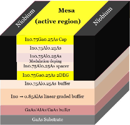
Figure 1. In0.75Ga0.25As/In0.75Al0.25As/GaAs heterostructure. The schematic view of the heterojunction where an In0.75Ga0.25As quantum well with 30 nm thickness is formed ⁓120 nm below the wafer surface. Nb was used as the superconducting contacts (shown in black) to form a hybrid and ballistic Nb–In0.75Ga0.25As 2DEG–Nb Josephson junction. Please click here to view a larger version of this figure.

Figure 2: On-chip hybrid superconducting-semiconducting quantum circuits. (a) SEM image of the QICs device showing a top view of a quantum circuit with 20 control wires, and 8 planar and symmetric JJs on a chip. The SEM image of Nb-In0.75Ga0.25As-Nb JJs with an In0.75Ga0.25As 2DEG gap of length L= 550 nm and 850 nm for e-beam lithographically (b) and photolithographically (c) fabricated junctions. Please click here to view a larger version of this figure.
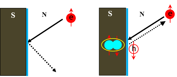
Figure 3. Normal and Andreev Reflections in hybrid superconducting-semiconducting junctions. (a) Specular quasiparticle reflection with no charge transmission through the interface. (b) Andreev reflection whereas the incoming electron is reflected as a hole in the opposite spin sub-band and transfer 2e charge into superconducting electrode. Please click here to view a larger version of this figure.
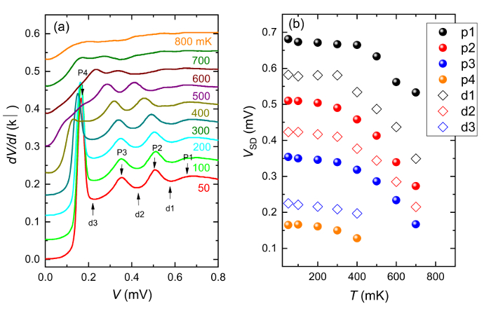
Figure 4. Induced superconductivity and SGS in In0.75Ga0.25As quantum wells in photolithographically fabricated junction. (a) Temperature dependence induced superconducting gap with pronounced SGS peaks due to multiple Andreev reflections. The SGS and the induced gap edge peaks, are marked by P1 to P4 while the SGS dips are marked by d1 to d3. (b) The SGS peaks and dips shown in (a) as a function of temperature. SGS are suppressed significantly at T> 400 mK leading to a shift toward zero bias. Please click here to view a larger version of this figure.
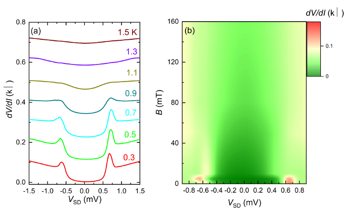
Figure 5. The temperature and magnetic field dependence of induced superconductivity in e-beam lithographically fabricated junctions. (a) Induced superconducting gap vs. applied source-drain voltage VSD at temperatures between 300 mK and 1.5 K. The curves are vertically offset for clarity. (b) Color-coded differential resistance as a function of VSD and perpendicular magnetic field at T= 300 mK. Please click here to view a larger version of this figure.
Discussion
On-chip QICs comprising an array of JJs based on superconducting indium gallium arsenide (In0.75Ga0.25As) quantum wells were demonstrated. Two important challenges of hybrid S-Sm material systems such as the scalability and interface transparency were addressed. Two critical steps whining the protocol including the growth of high quality and high mobility In0.75Ga0.25As two-dimensional electron gas in semiconducting heterostructures and proximity induced superconductivity into 2DEG were discussed23,24,25.
Growth of In0.75Ga0.25As with step-graded buffer layers in GaAs substrate and also the formation of homogeneous and barrier-free interfaces between the superconductor and semiconductor is a crucial step in such hybrid 2D quantum circuit development. It was demonstrated that with careful etching the sputtered superconducting film can make highly transparent contacts to In0.75Ga0.25As quantum wells resulting in detection of induced superconducting gap in semiconductors23,24,25.
The significance with respect to existing methods is that the presented technique for 2D hybrid JJs and circuit realization does not require the insitu deposition of superconductor on semiconductors in an MBE chamber after the semiconductor growth has been completed23,24,25. The other significance is that the heterostructure wafer can be grown as a desk of up to 10 cm diameter, allowing the fabrication of thousands of hybrid 2D junctions and circuits, so overcoming the scalability challenges of the hybrid S-Sm quantum circuits and devices22,23,24,25.
The induced superconductivity in quantum wells, SGS on differential conductance of the 2D junctions, and the phase coherent ballistic quantum transport measured in our junctions strongly suggest that hybrid 2D junctions and circuits based on superconducting In0.75Ga0.25As 2DEG afford promising material system for scalable quantum processing and computing technologies. Our approach may open a new road toward quantum technology and helps pave the way for the development of on-chip topological quantum circuits for realizing the next generation of quantum processors23,24,25.
Disclosures
The authors have nothing to disclose.
Acknowledgements
The authors acknowledge financial support from EPSRC, grant MQIC.
Materials
| Name | Company | Catalog Number | Comments |
|---|---|---|---|
| CompactDAQ Chassis | National Instruments | NI cDAC-9178 | |
| DSP Lock-in Amplifier | AMETEK 7265 | 190284-A-MNL-C | |
| Dilution refrigerator | Blueforce | Buttom loaded fridge | |
| Dilution refrigerator | Oxford | KelvinoxMX40 | Wet-fridge |
| Diamond scriber MICROTEC | Karl Suss | HR 100 | |
| Dektak Surface Profilometer | Veeco | 3ST | |
| Evaporator | Edwards | AUTO 306 | |
| Evaporator | Edwards | Coating system E306A | |
| 3He Cryostat | Oxford | ||
| Photoresist Spinner | Headway Research Inc. | EC101DT-R790 | |
| Matlab | |||
| Mask Aligner | Karl Suss | MJB 3 | |
| Source meter | Keithley | 2614B | |
| Semiconducting heterostructure | MBE Veeco | Gen III system | MBE Grown wafers |
| Wire Bonder | K&S | 4524 |
References
- Josephson, B. D. Possible new effects in superconductive tunneling. Physics Letters. 1, 251-253 (1962).
- Mukhanov, O. A. Energy-efficient single flux quantum technology. IEEE Transaction on Applied Superconductivity. 21, 760-769 (2011).
- Tsujimoto, M., et al. Broadly Tunable Subterahertz Emission from Internal Branches of the Current-Voltage Characteristics of Superconducting Bi2Sr2CaCu2O8+δ Single Crystals. Physical Review Letters. 108 (10), 1-5 (2012).
- Delfanazari, K., et al. Effect of Bias Electrode Position on Terahertz Radiation from Pentagonal Mesas of Superconducting Bi2Sr2CaCu2O8+d. IEEE Transaction Terahertz Science and Technology. 5 (3), 505-511 (2015).
- Delfanazari, K., et al. Terahertz Oscillating Devices Based upon the Intrinsic Josephson Junctions in a High Temperature Superconductor. Journal of Infrared, Millimeter, Terahertz Waves. 35 (1), 131-146 (2014).
- Delfanazari, K., et al. Tunable Terahertz Emission from the Intrinsic Josephson Junctions in Acute Isosceles Triangular Bi2Sr2CaCu2O8+δ Mesas. Optics Express. 21 (2), 2171-2184 (2013).
- Delfanazari, K., et al. Study of Coherent and Continuous Terahertz Wave Emission in Equilateral Triangular Mesas of Superconducting Bi2Sr2CaCu2O8+δ intrinsic Josephson Junctions. Physica C Superconductivity and its Application. 491, 16-19 (2013).
- Kashiwagi, T., et al. High Temperature Superconductor Terahertz Emitters: Fundamental Physics and Its Applications. Japanese Journal of Applied Physics. 51 (1), 1-14 (2012).
- Klemm, R. A., et al. Modeling the Electromagnetic Cavity Mode Contributions to the THz Emission from Triangular Bi2Sr2CaCu2O8+δ mesas. Physica C Superconductivity and its Application. 491, 30-34 (2013).
- Cerkoney, D. P., et al. Cavity Mode Enhancement of Terahertz Emission from Equilateral Triangular Microstrip Antennas of the High- Tcsuperconductor Bi2Sr2CaCu2O8+δ. Journal of Physics: Condensed Matter. 29 (1), 15601(2017).
- Sand-Jespersen, T., et al. Kondo-Enhanced Andreev Tunneling in InAs Nanowire Quantum Dots. Physical Review Letters. 99, 126603(2007).
- Herr, Q. P., et al. Reproducible operating margins on a 72800-device digital superconducting chip. Superconductor Science and Technology. 28, 124003(2015).
- Van Dam, J. A., Nazarov, Y. V., Bakkers, E. P. A. M., Franceschi, S. D., Kouwenhoven, L. P. Supercurrent reversal in quantum dots. Nature. 442, 667-670 (2006).
- Giazotto, F., et al. A Josephson Quantum Electron Pump. Nature Physics. 7, 857-861 (2011).
- Cybart, S. A., et al. Large voltage modulation in magnetic field sensors from two dimensional arrays of YBaCuO nano Josephson junctions. Applied Physics Letters. 104, 062601(2014).
- Kalhor, S., Ghanaatshoar, M., Kashiwagi, T., Kadowaki, K., Kelly, M. J., Delfanazari, K. Thermal Tuning of High- Tc Superconducting Bi2Sr2CaCu2O8+δ Terahertz Metamaterial. IEEE Photonics Journal. 9 (5), 1-8 (2017).
- Mourik, V., et al. Signatures of Majorana fermions in hybrid superconductor-semiconductor nanowire devices. Science. 336, 1003-1007 (2012).
- Chang, W., et al. Hard gap in epitaxial semiconductor-superconductor nanowires. Nature Nanotechnology. 10, 1038(2014).
- Rokhinson, L. P., Liu, X., Furdyna, J. K. The fractional ac. Josephson effect in a semiconductor-superconductor nanowire as a signature of Majorana particles. Nature Physics. 8, 795-799 (2012).
- Deng, M. T., et al. Majorana bound state in a coupled quantum-dot hybrid-nanowire system. Science. 354, 1557-1562 (2016).
- Gül, Ö, et al. Hard Superconducting Gap in InSb Nanowires. Nano Letters. 17 (4), 2690-2696 (2017).
- Nichele, F., et al. Scaling of Majorana Zero-Bias Conductance Peaks. Physical Review Letters. 119, 136803(2017).
- Delfanazari, K., et al. On Chip Andreev Devices: hard Gap and Quantum Transport in Ballistic Nb-In0.75Ga0.25As quantum well-Nb Josephson junctions. Advanced Materials. 29, 1701836(2017).
- Delfanazari, K., et al. Induced superconductivity in indium gallium arsenide quantum well. Journal of Magnetism and Magnetic Materials. 459, 282-284 (2018).
- Delfanazari, K., et al. On-chip hybrid Superconducting-Semiconducting Quantum Circuit. IEEE Transactions on Applied Superconductivity. 28, 4(2018).
- Chen, C., et al. Growth variations and scattering mechanisms in metamorphic In0.75Ga0.25As/In0.75Al0.25As quantum wells grown by molecular beam epitaxy. Journal of Crystal Growth. 425, 70-75 (2015).
- Blonder, G. E., Tinkham, M., Klapwijk, T. M. Transition from metallic to tunneling regimes in superconducting micro-constrictions: Excess current, charge imbalance, and supercurrent conversion. Physical Review B. 25, 4515(1982).
- Beenakker, C. W. J. Random-matrix theory of quantum transport. Review Modern Physics. 69, 731(1997).
Reprints and Permissions
